-
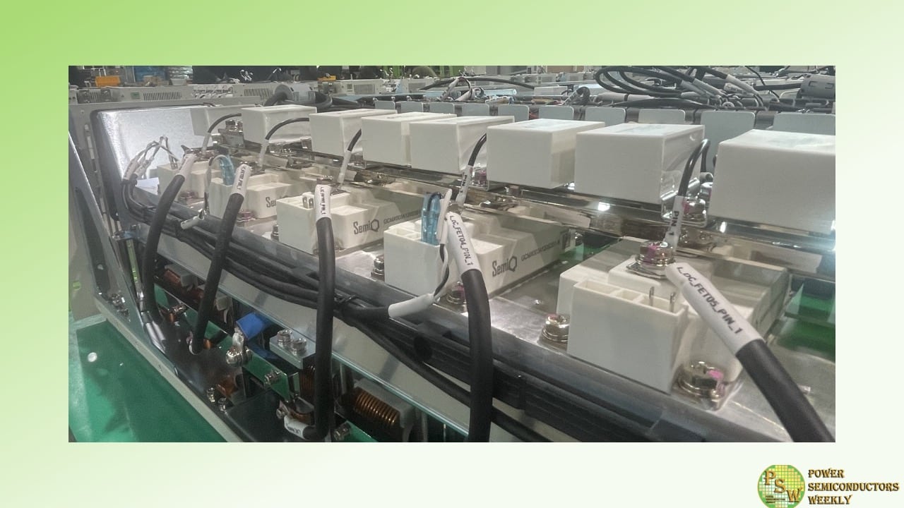
SemiQ Inc has begun shipping its SiC MOSFET modules for integration into advanced cell cycling systems used by several of the world’s leading battery manufacturers.
In lithium-ion batteries, cell cyclers enable the formation of a stable solid electrolyte interphase to enable increased longevity and performance. The systems also enable battery manufacturers to perform battery degradation analysis, temperature and stress testing, and check for defects or performance issues.
To undertake these tasks, the cyclers need to accurately charge and discharge batteries, with high switching frequencies enabling more precise control of current and voltage to avoid damage from overcharging/discharging. For this function, the MOSFETs need to withstand the thermal stress of repeated power cycling, with failure leading to test disruption and inaccurate data. Conversion efficiency is also vital in minimizing operational costs.
SemiQ is supplying its GCMX003A120S3B1-N and the GCMX003A120S7B1 QSiC™ 1200 V SiC half-bridge modules for use in 100 kW cyclers (10 x 10 kW cells with parallel connections).
These high-speed switching MOSFET modules are highly efficient with exceptionally low switching losses, are designed with a reliable body diode, have been tested to over 1350 V and implement a rugged design with easy mounting. Each 10 kW cell will integrate 12 modules, with 120 per 100 kW per cycler.
Dr. Timothy Han, President at SemiQ said: “Reports show that the electrification of transportation is among the most important steps that can be taken to reach net-zero. For this, the evaluation of battery performance, durability, and efficiency plays a vital role in enabling the development of longer-range, longer-life EV batteries. We’re delighted to be working with one of the world’s leading cell cyclers and this partnership is testament to the ruggedness and efficiency of our SiC technology.”
Datasheets for the GCMX003A120S3B1-N and GCMX003A120S7B1 modules can be downloaded via the product page, here.
Original – SemiQ
-

Nexperia introduces a range of highly efficient and robust industrial grade 1200 V silicon carbide (SiC) MOSFETs with industry leading temperature stability in innovative surface-mount (SMD) top-side cooled packaging technology called X.PAK. This package, with its compact form factor of 14 mm x 18.5 mm, combines the assembly benefits of SMD with the cooling efficiency of through-hole technology, ensuring optimal heat dissipation.
This release addresses the growing demand from a broad range of high power (industrial) applications for discrete SiC MOSFETs that harness the advantages of top-side cooling to deliver exceptional thermal performance. These switches are ideal for industrial applications such as battery energy storage systems (BESS), photovoltaic inverters, motor drives, and uninterruptible Power Supplies (UPS). Additionally, they are well-suited for electric vehicle charging infrastructure, including charge piles.
The X.PAK package further enhances the thermal performance of Nexperia’s SiC MOSFETs by reducing the negative impacts of heat dissipation via the PCB. Furthermore, Nexperia’s X.PAK package enables low inductance for surface mount components and supports automated board assembly.
The new X.PAK packaged devices deliver class-leading figures-of-merit (FoM) known from Nexperia SiC MOSFETs, with RDS(on) being a particularly critical parameter due to its impact on conduction power losses. However, many manufacturers concentrate on the nominal value of this parameter and neglect the fact that it can increase by more than 100% as device operating temperatures rise, resulting in significant conduction losses. Nexperia SiC MOSFETs, on the other hand, offer industry-leading temperature stability, with the nominal value of RDS(on) increasing by only 38% over an operating temperature range from 25 °C to 175 °C.
“The introduction of our SiC MOSFETs in X.PAK packaging marks a significant advancement in thermal management and power density for high-power applications,” said Katrin Feurle, Senior Director and Head of SiC Discretes & Modules at Nexperia. “This new top-side cooled product option builds on our successful launches of discrete SiC MOSFETs in TO-247 and SMD D2PAK-7 packages. It underscores Nexperia’s commitment to providing our customers with the most advanced and flexible portfolio to meet their evolving design needs.”
The initial portfolio includes products with RDS(on) values of 30, 40, 60 mΩ (NSF030120T2A0, NSF040120T2A1, NSF060120T2A0), a part with 17 mΩ will be released in April 2025. An automotive qualified SiC MOSFETs portfolio in X.PAK packaging will follow later in 2025, as well as further RDson classes like 80 mΩ.
Original – Nexperia
-
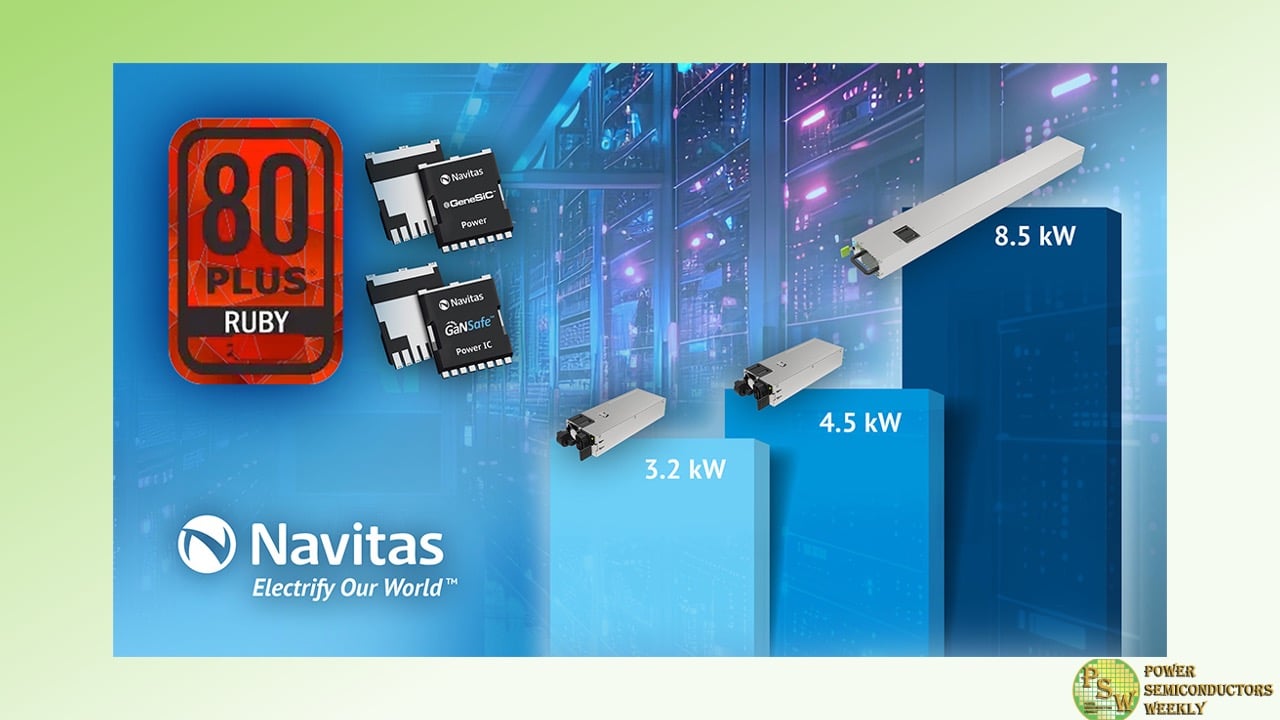
Navitas Semiconductor has announced that its portfolio of 3.2kW, 4.5kW, and 8.5 kW AI data center power supply unit (PSU) designs exceed the new 80 PLUS ‘Ruby’ certification, focused on the highest level of efficiency for redundant server data center PSUs.
The 80 PLUS certification program assesses and certifies the energy efficiency of internal PSUs in computers and servers. The ‘Ruby’ certification was announced in January 2025 by 80 PLUS’s administrating body, CLEAResult, following its endorsement by the Green Grid consortium.
‘Ruby’ is the most rigorous PSU efficiency standard since the ‘Titanium’ certification was released 14 years ago. In comparison, Ruby sets an additional 1% system efficiency across all load conditions, except at 50% load (which requires a 0.5% increase), to achieve a new benchmark of 96.5% efficiency.
This new standard offers the industry a clear path to enhanced energy efficiency, helping data centers address the evolving needs of cloud storage, commercial sectors, and the increasing pressure on the grid from AI computing. For example, every Ruby-certified 3.2 kW CRPS185 PSU can save up to 420 kilowatt-hours during a 3-year lifetime. That is the equivalent of over 400 kg of CO2 emissions.
Navitas exceeds both Ruby and Titanium certifications on their portfolio of AI data center PSU reference designs, ranging from 3.2 kW to 8.5 kW, and are powered by high-power GaNSafe™ ICs and GeneSiC™ Gen 3 ‘Fast’ SiC MOSFETs.
Navitas is the established leader in AI data center solutions enabled by GaN and SiC technology. In August 2023, they introduced a high-speed, high-efficiency 3.2 kW CRPS, achieving a 40% smaller size than best-in-class, legacy silicon solutions for power-hungry AI and Edge computing. This was followed by the world’s highest power density 4.5 kW CRPS, achieving a ground-breaking 137 W/in3, and efficiency of over 97%.
In November 2024, Navitas released the world’s first 8.5 kW AI data center power supply powered by GaN and SiC that could meet 98% efficiency, complying with the Open Compute Project (OCP) and Open Rack v3 (ORv3) specifications. Additionally, Navitas created IntelliWeave, an innovative patented new digital control technique, that when combined with high-power GaNSafe and Gen 3-Fast SiC MOSFETs, enables PFC peak efficiencies to 99.3% and reduces power losses by 30% reduction compared to existing solutions.
“Compared with Titanium, Ruby cuts the allowable PSU losses significantly and will be critical in enabling the data center industry to reduce its carbon footprint and cut operational costs,” said Gene Sheridan, CEO and co-founder of Navitas. “With the industry set to consume 1,000 TWh annually by next year1, every percentage point improvement in efficiency represents a reduction of 10 TWh, or approximately 3.5 million tons of CO22. Advances in our GaNFast and GeneSiC products enable these targets to be met and significantly exceeded.”
Navitas’ AI Power Roadmap and 80 PLUS Ruby-compliant demos can be viewed at the ‘Planet Navitas’ booth #1107 during the APEC 2025 conference, which takes place at Atlanta’s Georgia World Congress Center from March 16 to 20.
Original – Navitas Semiconductor
-

onsemi introduced the first generation of its 1200V silicon carbide (SiC) metal oxide semiconductor field-effect transistor (MOSFET) based SPM 31 intelligent power modules (IPMs). onsemi EliteSiC SPM 31 IPMs deliver the highest energy efficiency and power density in the smallest form factor compared to using Field Stop 7 IGBT technology, resulting in lower total system cost than any other leading solution on the market.
Their improved thermal performance, reduced power losses and ability to support fast switching speeds makes these IPMs ideally suited for three-phase inverter drive applications such as electronically commutated (EC) fans in AI data centers, heat pumps, commercial HVAC systems, servo motors, robotics, variable frequency drives (VFDs), and industrial pumps and fans.
The EliteSiC SPM 31 IPMs offer several current ratings from 40A to 70A. Complemented by onsemi’s IGBT SPM 31 IPM portfolio, covering low currents from 15A to 35A, onsemi now provides the industry’s broadest range of scalable and flexible integrated power module solutions in a small package.
In 2023, operations of residential and commercial buildings accounted for 27.6% of U.S. end-use energy consumption. As electrification and AI adoption grow, particularly with the construction of more AI data centers increasing energy demands, the need to reduce the energy consumption of applications in this sector is becoming more critical. Power semiconductors capable of efficiently converting electric power are the key in this transition to a low-carbon-emissions world.
With the number and size of data centers growing, the demand for EC fans is expected to rise. These cooling fans maintain the ideal operating environment for all equipment in a data center and are essential for accurate, error-free data transmission. The SiC IPM ensures the EC fan operates reliably and at its highest efficiency.
Like many other industrial applications such as compressor drives and pumps, EC fans require higher power density and efficiency than existing larger IGBT solutions. By switching to EliteSiC SPM 31 IPMs, customers can benefit from a smaller footprint, higher performance, and a simplified design due to high integration, resulting in shortened development time and lower total system cost in addition to reduced GHG emissions. For example, compared to a system solution that uses a current IGBT power integrated module (PIM) with power losses of 500W at 70% load, implementing highly efficient EliteSiC SPM 31 IPMs could reduce the annual energy consumption and cost per EC fan by 52%.
The fully integrated EliteSiC SPM 31 IPM consists of an independent high side gate driver, low voltage integrated circuit (LVIC), six EliteSiC MOSFETs and a temperature sensor (voltage temperature sensor (VTS) or thermistor). The module is based on the industry-leading M3 SiC technology that shrinks die size and is optimized for hard-switching applications with improved short-circuit withstand time (SCWT) performance when used in the SPM 31 package, making them suitable for inverter motor drives for industrial use. The MOSFETs are configured in a three-phase bridge with separate source connections for the lower legs for maximum flexibility in the choice of control algorithm.
In addition, the EliteSiC SPM 31 IPMs include the following benefits:
- Low loss, short-circuit-rated M3 EliteSiC MOSFETs to prevent catastrophic equipment and component failures such as electric shock or fire.
- Built-in under-voltage protection (UVP) to protect against damage to the device when voltage is low.
- As the peer-to-peer product of FS7 IGBT SPM 31, customers can choose between various current ratings while using the same PCB board.
- UL certified to meet national and international safety standards
- Single-grounded power supply offering better safety, equipment protection and noise reduction.
- Simplified design and reduced size of customer boards due to
- Included controls for gate drivers and protections
- Built-in bootstrap diodes (BSDs) and resistors (BSRs)
- Internal boost diodes provided for high side gate boost drive
- Integrated temperature sensor (VTS output by LVIC and/or thermistor)
- Built-in high-speed high-voltage integrated circuit
Original – onsemi
-

Many industrial applications today are moving towards higher power levels with minimized power losses. One way to achieve this is to increase the DC link voltage. Infineon Technologies AG is addressing this market trend with the CoolSiC™ Schottky diode 2000 V G5 product family, the first discrete silicon carbide diodes with a breakdown voltage of 2000 V, introduced in September 2024.
The product portfolio has now been expanded to include a Schottky diode in the TO-247-2 package, which is pin-compatible with most existing TO-247-2 packages. The product family fits perfectly for applications with DC link voltages up to 1500 V DC, making it ideal for solar and EV chargers.
The CoolSiC Schottky diode 2000 V G5 in the TO-247-2 package is available with current ratings ranging from 10 to 80 A. It allows developers to achieve higher power levels in their applications while reducing the component count by half compared to 1200 V solutions. This simplifies the overall design and facilitates a seamless transition from multi-level to two-level topologies.
In addition, the Schottky diode in the TO-247-2 package incorporates .XT interconnection technology, which significantly reduces thermal resistance and impedance, thereby enhancing heat management. Humidity robustness has been validated through HV-H3TRB reliability testing. The diodes exhibit neither reverse recovery nor forward recovery, and feature a low forward voltage, ensuring improved system performance.
The 2000 V diode family is a perfect match for the CoolSiC MOSFETs 2000 V in the TO-247Plus-4 HCC package that Infineon launched in the spring of 2024. In addition to the TO-247-2 package, the CoolSiC Schottky Diode 2000 V is also available in the TO-247PLUS-4 HCC package.
Original – Infineon Technologies
-
NoMIS Power has announced a major breakthrough in improving the short-circuit withstand time (SCWT) of SiC MOSFETs. This innovation addresses one of the key challenges limiting the widespread adoption of SiC technology in high-power applications.
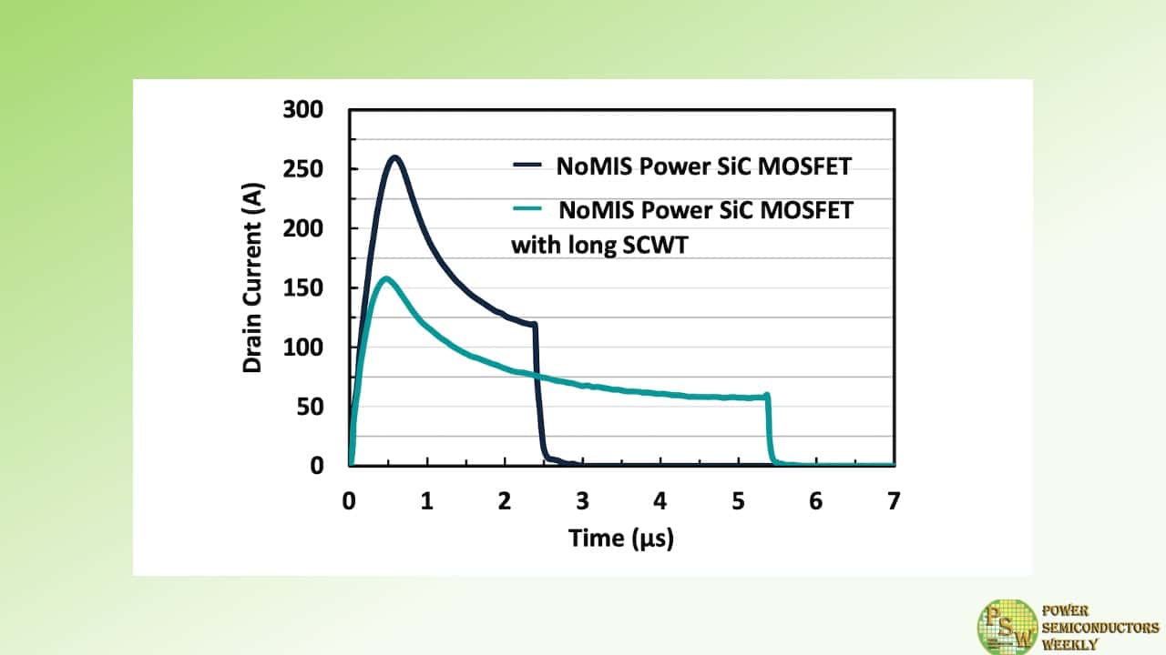
Silicon carbide (SiC) devices have gained prominence in power electronics due to their high efficiency, fast switching, and superior thermal performance. However, their historically lower short-circuit robustness compared to silicon-based IGBTs has posed challenges for their use in high-voltage and high-reliability environments, such as industrial drives, electric vehicles, and grid applications. NoMIS Power’s latest advancement significantly extends the SCWT of SiC MOSFETs to a minimum of 5 µs (Fig. 1), compared to the current industry standard of 2-3 µs, with no deleterious effect on specific on-resistance (Ron,sp) (Fig. 2). This enhancement greatly improves reliability and unlocks new opportunities for system designers seeking to maximize performance while maintaining fault tolerance.
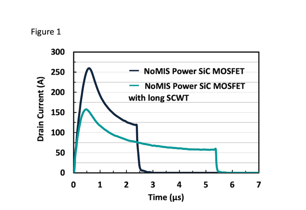
Figure 1: Drain currents of the NoMIS Power SiC MOSFET and NoMIS Power SiC MOSFET with long SCWT under short-circuit conditions right before failure. Drain currents of the 1.2 kV, 80 mΩ SiC MOSFET (dark blue) and the long SCWT 1.2 kV, 80 mΩ SiC MOSFET (light blue) from NoMIS Power are compared. The measurement for short-circuit was conducted under the following conditions: Rg of 20 Ω, Vgs of 20 V, and a Vds of 800 V.
By tuning the trade-off between Ron,sp and SCWT using NoMIS Power’s proprietary SiC MOSFET fabrication design and process flow, the performance shown in Fig. 1 & Fig. 2 was achieved; and can be similarly managed depending on the specific application. Complete optimization of SiC MOSFETs with long SCWT using this approach will allow NoMIS Power to further extend the SCWT while maintaining negligible impact on Ron,sp.
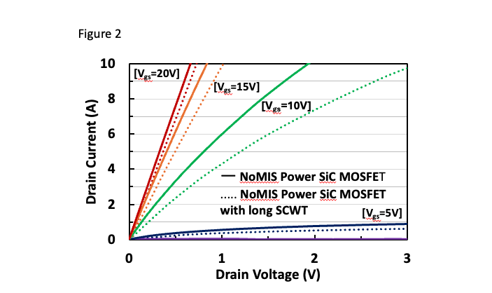
Figure 2: Typical output characteristics of NoMIS Power 1.2 kV, 80 mQ SiC MOSFET and NoMIS Power 1.2 kV, 80 mQ SiC MOSFET with long SCWT showing no significant negative impact on on-resistance.
“At NoMIS Power, we have focused extensively on device architecture engineering, leading to a significant advancement in SiC short-circuit withstand time,” said Woongje Sung, CTO at NoMIS Power. “We believe this achievement provides valuable advantages to the power electronics community, helping engineers integrate SiC solutions with greater confidence in applications where robustness is critical.”
NoMIS Power’s long SCWT devices are well-screened for latent defects and offer easier gate driver desaturation (dSat) design for high di/dt and dv/dt, enabling faster switching frequencies of up to hundreds of kHz. Initial test results demonstrate a 2X to 4X increase in short-circuit withstand time compared to existing SiC devices, positioning NoMIS Power’s technology as a frontrunner in the next generation of power semiconductors. Additionally, when coupled with packaging innovations that impact junction-to-case thermal capacitance, alongside novel thermal management techniques with high heat transfer coefficients, the overall SCWT of the SiC MOSFET can be further improved.
The impact of this innovation extends across multiple industries, including renewable energy, electric transportation, and high-power industrial applications. A longer short-circuit withstand time ensures rugged and reliable performance in critical applications, reinforcing the robustness of SiC-based power systems. For example, built-in redundancy of the SiC MOSFETs inside power converters, which impacts costs as well as power density, can be reduced. Furthermore, applications sensitive to electromagnetic inference, that cannot solely rely on digital control and sensing schemes to detect and act upon short-circuit events, will now be able to effectively utilize SiC MOSFETs with lower risk. As SiC adoption accelerates, NoMIS Power’s breakthrough will play a pivotal role in enhancing the reliability and safety of SiC-based power converters and systems.
NoMIS Power is showcasing this breakthrough technology at APEC 2025, March 16-20, Atlanta, GA, Booth 548 along with its expanded range of SiC discretes and power modules.
Original – NoMIS Power
-

Leapers Semiconductor has officially commenced construction of its automotive-grade third-generation power semiconductor module project in Jiangdu District’s development zone. The launch event was part of Jiangdu District’s Major Project Construction Mobilization Conference, where local officials outlined key economic initiatives for the region. District Party Secretary Zhu Lili delivered a speech at the ceremony, emphasizing the urgency of driving economic growth from the start of the year. District Mayor Shen Bohong presided over the event, with key government representatives also in attendance.
During the event, township leaders provided updates on the district’s 2025 major construction projects, reaffirming their commitment to economic development. The first quarter alone saw the initiation of 29 major projects, with a total investment of 8.72 billion yuan ($1.2 billion), spanning sectors such as new materials, renewable energy, high-end equipment, and environmental protection.
Leapers Semiconductor SiC module project, which began construction on March 1, represents a 10 billion yuan ($1.4 billion) investment, covering an area of 32 acres. Once completed, the facility is expected to achieve an annual production capacity of 3 million automotive-grade SiC modules, generate 10 billion yuan ($1.4 billion) in annual revenue, and contribute 500 million yuan ($70 million) in annual tax revenue.
With this new SiC module packaging and testing facility, Leapers Semiconductor is set to enhance production capabilities, accelerate innovation, and drive the adoption of SiC power solutions worldwide.
Original – Leapers Semiconductor
-
 LATEST NEWS / PRODUCT & TECHNOLOGY / PROJECTS / SiC / TOP STORIES / WBG
February 27, 2025
4 Min ReadSilicon carbide (SiC) provides considerable technical advantages for power electronics – however, the costs are still a drawback. In the »ThinSiCPower« research project, a consortium of Fraunhofer Institutes is developing key technologies to reduce material losses and device thickness while increasing the thermomechanical stability of the assembled SiC chips. The savings achieved are expected to help further accelerate the market development of efficient SiC power electronics.
Power electronics based on the wide-bandgap semiconductor silicon carbide (SiC) are a key enabler for energy-efficient, sustainable and high-performance applications in electromobility – from cars and commercial vehicles to trains, ships and airplanes, in the generation, transportation and storage of renewable energies, as well as for IT and industrial infrastructures. It is therefore an important and competitively relevant factor for the current global transformation processes in the areas of mobility, energy and digitalization. The market for SiC power devices is expected to grow at an annual rate of over 30 percent. Compared to conventional silicon technology, the use of SiC power electronics in a standard drive converter saves more energy than is required to manufacture the SiC power electronics themselves.
While the technological advantages of SiC are obvious due to its physical properties, the higher costs compared to the established silicon are still an obstacle to faster market penetration. Chip costs are more than three times higher than for silicon. The initially required SiC wafer is the biggest cost driver here. In the case of a SiC-based metal-oxide semiconductor field-effect transistor (MOSFET), this accounts for more than 40 percent of the manufacturing costs. In addition, due to the unfavorable mechanical material properties and large thickness of the monocrystalline SiC wafer, electronics processed from it only achieve approx. 30 percent of the thermomechanical service life compared to silicon. This disadvantage leads to an approx. 25 percent larger chip area and, in the case of an inverter for example, to around 25 percent higher costs in the application.
In the three-year ThinSiCPower project (2024-2027), funded by the Fraunhofer PREPARE program, researchers are developing an alternative way to produce cost-effective SiC substrates and significantly thinner SiC chips using more resource-efficient processing technologies. Rather than first sawing the expensive, high-quality SiC wafers with the usual material loss and later back-grinding them in device processing, the SiC crystal is separated directly into thinner wafers using a special laser process without any major loss of material, which are then bonded onto an inexpensive carrier substrate based on polycrystalline SiC.
Fraunhofer ISE, ENAS and IWM with the Fraunhofer IISB as project coordinator are pooling their individual competencies in ThinSiCPower. A SiC coating technology developed by Fraunhofer IISB is being adapted for the manufacturing of the poly-SiC carrier substrates, which is more cost- and resource-efficient than the conventional manufacturing method using chemical vapor deposition. The low-loss separation of the thin SiC wafers is carried out using a laser for defined mechanical pre-damage (Fraunhofer ISE) and subsequent separation under well-defined mechanical conditions for controlled crack propagation (Fraunhofer IWM).
The wafer bonding process for the poly-SiC substrate with the split SiC, including the necessary surface preparation before and after the bonding process, will be developed at Fraunhofer ENAS, while the subsequent device processing and qualification will take place at Fraunhofer IISB. The partners are also developing adapted electrical test methods at thin wafer level as well as physics-of-failure simulation models to maximize the market acceptance of this new class of low-cost SiC substrates. With this, a broad applicability in the relevant industries could be achieved.
The aim is to reduce SiC device costs by 25 percent by developing technology for the production of costeffective thin SiC wafers and poly-SiC substrates. In addition, SiC design costs are to be reduced by further 25 percent by increasing the load cycle stability by 300 percent. The target markets are semiconductor and power module manufacturers as well as their process and equipment suppliers through to test equipment suppliers. With this project, the participating partner institutes are also combining their expertise to set up a complete, highly innovative and future-oriented SiC processing line within the Research Fab Microelectronics Germany (FMD). The consortium is receiving consultancy support directly from partners in industry.
The ThinSiCPower project not only accelerates the market penetration of silicon carbide through the targeted cost reduction and conceptual advantages, but also serves to secure an innovative, resilient and industry relevant SiC technology value chain in Germany and Europe.
Original – Fraunhofer IISB
-

SemiQ Inc will give the first official unveiling of the company’s new 1700 V and 1200 V Gen 3 SiC MOSFETs at the 2025 Applied Power Electronics Conference (APEC).
APEC takes place at the Georgia World Congress Center in Atlanta from March 16, with SemiQ’s booth located at stand #1348.
SemiQ’s 1200 V Gen3 SiC was announced in February, delivering an improved performance with a smaller die size and at a lower cost. The series includes automotive qualified (AEC-Q101) options and Known Good Die (KGD) testing has been implemented across the series with verification at voltages exceeding 1400 V, plus avalanche testing to 800 mJ. Reliability is further improved through 100% gate-oxide burn-in screening and UIL testing of discrete packaged devices.
The company’s new 1700 V MOSFET family of MOSFETS and modules with AEC-Q101 certification is designed to meet the needs of medium-voltage high power conversion applications, from photovoltaic, wind inverters and energy storage to EV and roadside charging as well as uninterruptable power supplies, and induction heating/welding. These switching planar D-MOSFETs enable more compact system designs with higher power densities and have been tested to KGD beyond 1900 V, with UIL avalanche testing to 600 mJ.
Dr. Timothy Han, President at SemiQ said: “There is so much innovation happening in power electronics right now and we’re delighted to have launched our next generation technologies in time to have them on display at APEC. The show brings together many of the leading minds within the industry and we’re looking forward to discussing the challenges faced and how we can help them.”
Original – SemiQ
-
SemiQ Inc has announced a family of three 1200V SiC full-bridge modules, each integrating two of the company’s rugged high-speed switching SiC MOSFETs with reliable body diode. The modules have been developed to simplify the development of photovoltaic inverters, energy storage, battery charging and other high-frequency DC applications.
Available in 18, 38 and 77mΩ (RDSon) variants, the modules have been tested at voltages exceeding 1350V and deliver a continuous drain current of up to 102A, a pulsed drain current of up to 250A and a power dissipation of up to 333W.
Operational with a junction temperature of up to 175oC, the rugged B2 modules have exceptionally low switching losses (EON 0.13mJ, EOFF 0.04mJ at 25oC – 77mΩ module), low zero-gate voltage drain/gate source leakage (0.1µA/1nA – all modules) and low junction to case thermal resistance (0.4oC per watt – 18mΩ module).
“By integrating high-speed SiC MOSFETs with exceptional performance and reliability, our new QSiC 1200V family of full-bridge modules sets a new standard for power density and efficiency in demanding DC applications. This family of modules simplifies system design, and enables faster time-to-market for next-generation solar, storage, and charging solutions,” said Seok Joo Jang, Director of Module Engineering at SemiQ.
Available immediately, the modules can be mounted directly to a heat sink, are housed in a 62.8 x 33.8 x 15.0mm package (including mounting plates) with press fit terminal connections and split DC negative terminals.
Original – SemiQ
