-

Navitas Semiconductor announced their AI data center technology roadmap for up to 3x power increase to support similar exponential growth in AI power demands expected in just the next 12-18 months.
Traditional CPUs require typically only 300W and the data center ac/dc power supplies would typically power the equivalent of 10 of these or 3,000W (3kW). High-performance AI processors like NVIDIA’s ‘Grace Hopper’ H100 are already demanding 700W each today, with next-gen ‘Blackwell’ B100 & B200 chips anticipated to increase to 1,000W or more by next year.
To meet this exponential power increase, Navitas is developing server power platforms which rapidly increase from 3kW to up to 10kW. In August 2023, Navitas introduced a 3.2kW data center power platform utilizing latest GaN technology enabling over 100W/in3 and over 96.5% efficiency. Now, Navitas is releasing a 4.5kW platform enabled by a combination of GaN and SiC to push densities over 130W/in3 and efficiencies over 97%. These two platforms have already generated significant market interest with over 20 data center customer projects in development expected to drive millions in GaN or SiC revenues starting this year.
Today, Navitas also announces its plans to introduce an 8-10kW power platform by the end of 2024 to support 2025 AI power requirements. The platform will utilize newer GaN and SiC technologies and further advances in architecture to set all-new industry standards in power density, efficiency and time-to-market. Navitas is already engaged with major data-center customers, with full platform launch anticipated in Q4 ’24, completing this 3x increase in power demands in only 12-18 months.
Navitas’ unique data-center design center is creating these system designs to address the dramatic increases in AI data center power requirements, and assist customers to deploy platforms quickly and effectively to meet the accelerated time-to-market demands of rapid AI advances. System designs include complete design collateral with fully-tested hardware, schematics, bill-of-materials, layout, simulation and hardware test results to maximize first-time-right designs and fast revenue generation.
“The rapid development and deployment of artificial intelligence (AI) into global data centers has created a dramatic and unexpected power challenge for our entire industry,” noted Gene Sheridan, Navitas’ CEO and Co-Founder. “Our investment in leading-edge GaN and SiC technologies, combined with our unique data-center design center capabilities, have positioned us well. Our team has really stepped up to the challenge, with a 3x power increase in less than 18 months.”
Original – Navitas Semiconductor
-
 LATEST NEWS / PROJECTS / SiC / WBG
Tianjin Economic-Technological Development Area Inked Investment Agreement with Vitesco Technologies
March 8, 2024
1 Min ReadTianjin Economic-Technological Development Area (TEDA) inked an investment agreement with Vitesco Technologies for a new project for NEV intelligent manufacturing and automotive electronic products. With the new project, Vitesco aims to strengthen its presence in TEDA by introducing new products such as silicon carbide power modules, 800V motor stators and rotors, EMR3 three-in-one axle drive systems, high-voltage inverters, battery control units, and gearbox controllers.
Vitesco Technologies is a global leader in automotive technology development and manufacturing, dedicated to providing advanced driving technology for sustainable mobility. Vitesco Technologies has been cooperating with TEDA for many years.
The establishment of its R&D center in TEDA in 2019 marks a major step forward in the NEV market, upgrading the Vitesco Tianjin Base into a super factory integrating R&D, testing, and production. Thomas Stierle, member of the Executive Board and head of Electrification Solutions Division of Vitesco Technologies, expressed confidence in China, Tianjin, and TBNA. He stated that Vitesco Technologies will continue to increase its investment in TBNA and deepen cooperation in manufacturing R&D and technological innovation.
-

Toshiba Electronic Devices & Storage Corporation has started mass production of a 3rd generation silicon carbide (SiC) 1700 V and drain current (DC) rating 250 A of SiC MOSFET module “MG250V2YMS3” for industrial equipment and has expanded its lineup.
The new product MG250V2YMS3 offers low conduction loss with low drain-source on-voltage (sense) of 0.8 V (typ.). It also offers low switching loss with low turn-on switching loss of 18 mJ (typ.) and low turn-off switching loss of 11 mJ (typ.). This helps to reduce power loss of equipment and the size of cooling device.
MG250V2YMS3 has a low stray inductance of 12 nH (typ.) and is capable of high-speed switching. In addition, it suppresses surge voltage in switching operation. Thus, it is available for high frequency isolated DC-DC converter.
Toshiba’s SiC MOSFET module of 2-153A1A package has a lineup of four existing products, MG250YD2YMS3 (2200 V / 250 A), MG400V2YMS3 (1700 V / 400 A), and MG600Q2YMS3 (1200 V / 600 A), including new products. This provides a wider range of product selection.
Toshiba will continue to meet the needs for high efficiency and the downsizing of industrial equipment.
Applications
Industrial equipment
- Inverters and converters for railway vehicles
- Auxiliary power supply for railway vehicles
- Renewable energy power generation systems
- Motor control equipment for industrial equipment
- High frequency DC-DC converters, etc.
Features
- Low drain-source on-voltage (sense):
VDS(on)sense=0.8 V (typ.) (ID=250 A, VGS=+20 V, Tch=25 °C) - Low turn-on switching loss:
Eon=18 mJ (typ.) (VDD=900 V, ID=250 A, Tch=150 °C) - Low turn-off switching loss:
Eoff=11 mJ (typ.) (VDD=900 V, ID=250 A, Tch=150 °C) - Low stray inductance:
LsPN=12 nH (typ.)
Original – Toshiba
-
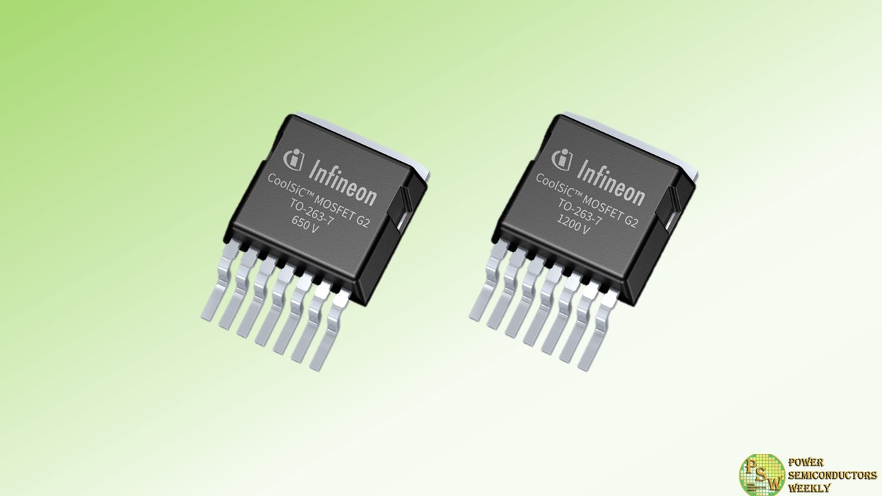
Infineon Technologies AG opens a new chapter in power systems and energy conversion and introduces the next generation of silicon carbide (SiC) MOSFET trench technology. The new Infineon CoolSiC™ MOSFET 650 V and 1200 V Generation 2 improve MOSFET key performance figures such as stored energies and charges by up to 20 percent compared to the previous generation without compromising quality and reliability levels leading to higher overall energy efficiency and further contributing to decarbonization.
CoolSiC MOSFET Generation 2 (G2) technology continues to leverage performance capabilities of silicon carbide by enabling lower energy loss that turns into higher efficiency during power conversion. This provides strong benefits to customers for various power semiconductor applications such as photovoltaics, energy storage, DC EV charging, motor drives and industrial power supplies.
A DC fast charging station for electric vehicles which is equipped with CoolSiC G2 allows for up to 10 percent less power loss compared to previous generations, while enabling higher charging capacity without compromising form factors. Traction inverters based on CoolSiC G2 devices can further increase electric vehicle ranges. In the area of renewable energies, solar inverters designed with CoolSiC G2 make smaller sizes possible while maintaining a high power output, resulting in a lower cost per watt.
“Megatrends call for new and efficient ways to generate, transmit and consume energy. With the CoolSiC MOSFET G2, Infineon brings silicon carbide performance to a new level,” said Dr. Peter Wawer, Division President Green Industrial Power at Infineon.
“This new generation of SiC technology enables the accelerated design of more cost-optimized, compact, reliable, and highly efficient systems harvesting energy-savings and reducing CO 2 for every watt installed in the field. It’s a great example of Infineon’s relentless spirit, constantly pushing for innovation to drive decarbonization and digitalization in the industrial, consumer and automotive sectors.”
Contributing to high-performance CoolSiC G2 solutions, Infineon’s pioneer CoolSiC MOSFET trench technology provides an optimized design trade-off, allowing higher efficiency and reliability compared to SiC MOSFET technology available so far. Combined with the award-winning .XT packaging technology, Infineon is further increasing the potential of designs based on CoolSiC G2 with higher thermal conductivity, better assembly control and improved performance.
Mastering all relevant power technologies in silicon, silicon carbide and gallium nitride (GaN), Infineon offers design flexibility and leading-edge application know-how that meet the expectations and demands of modern designers. Innovative semiconductors based on wide-bandgap (WBG) materials like SiC and GaN are the key to conscious and efficient use of energy in fostering decarbonization.
Original – Infineon Technologies
-
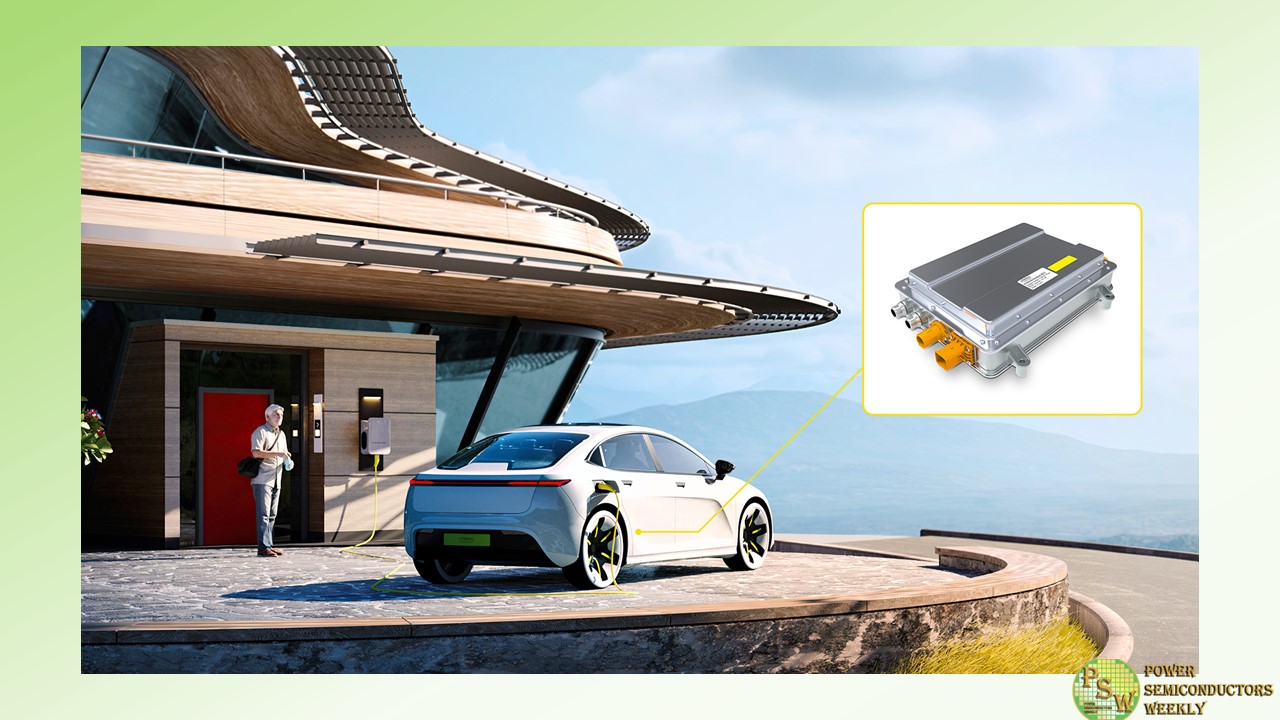
Vitesco Technologies is preparing the series application of its High Voltage Box. The modular system makes charging, converting and distributing electricity in electric vehicles cheaper by integrating several functions in one unit, depending on the design.
This includes the vehicle On-Board Charger for AC charging on the grid with up to 22 kW of charging power, a DC current converter providing the current for the 12 V vehicle net, and power electronics which distribute high voltage power in the vehicle and facilitate fast DC-charging with up to 800 V.
Owed to the high level of mechatronic integration, the High Voltage Box has smaller space requirements to the vehicle while increasing the total system reliability in comparison to individual devices. State-of-the art silicon carbide (SiC) semiconductors boost charging efficiency to over 95 percent which lowers the vehicle owner’s electricity bill. This efficiency level is particularly beneficial for car owners because electric vehicles are frequently charged on the grid.
Due to the high AC charging rate of up to 22 kW the High Voltage Box charges the car with 200 km of range in under two hours. DC high-power charging with up to 800 V achieves the same range in 12 minutes. The sophisticated power electronics ensure that this system offers electrical safety as well as efficiency.
On a day-to-day level, charging, energy conversion and power distribution are just as relevant for a driver’s satisfaction with a vehicle as driving itself is. With our High Voltage Box, we integrate these core tasks of energy management into one efficient and compact unit. This integration makes electrification on a large scale and at low cost easier.
Thomas Stierle, Member of the Executive Board and head of the Electrification Solutions division of Vitesco Technologies
Today, the so-called On-Board Charger (OBC) for charging with alternating current (AC) on the grid is a separate device in the vehicle. This OBC inverts grid power to direct current (DC) that can be fed to the high voltage battery. Another separate device is the DC/DC converter which provides direct current from the high voltage battery to the 12 V power net – or it boosts 12 V to high voltage DC. A power electronics unit distributes high voltage current within the vehicle (hence: Power Distribution Unit, PDU). In addition, these electronics can be designed to allow DC charging with up to 800 V at high power charging points. All those components need to be connected, they require a housing, installation space, and cooling.
The modular and scalable High Voltage Box makes it easier to cover two or more of these functions with a single device. SiC technology is used to minimize the conversion losses of the unit:
A high level of efficiency brings the car owner’s electricity bill down and contributes to sustainability.
Christian Preis, Head of Base Development Energy Transformation at Vitesco Technologies
Within the modular design Vitesco Technologies covers all relevant European and worldwide grid topologies. The High Voltage Box was developed to support modular vehicle adaptation for the global market. At the same time, Vitesco Technologies is driving new functions ahead. The High Voltage Box for one of the two series applications will already function bidirectionally so that it can supply alternating current with 230 V from the DC battery current when this is required.
This puts vehicle owners in the comfortable position to make versatile use of their large battery. For instance, if they wish to use power tools far away from the grid, or if they want to feed electricity to the grid which they have charged earlier from their own photovoltaic system. “In the future, this option to stabilize the grid will continue to gain importance “, Preis adds. The company’s experts are advancing the necessary standard for this in key committees and are thus part of the decision-making process about development trends.
In the future the High Voltage Box with bidirectional function can also make it possible to power a whole house from the High Voltage Battery during a blackout. This is an option because batteries in vehicles have a much bigger capacity than most of the batteries typically installed in private homes.
Original – Vitesco Technologies
-
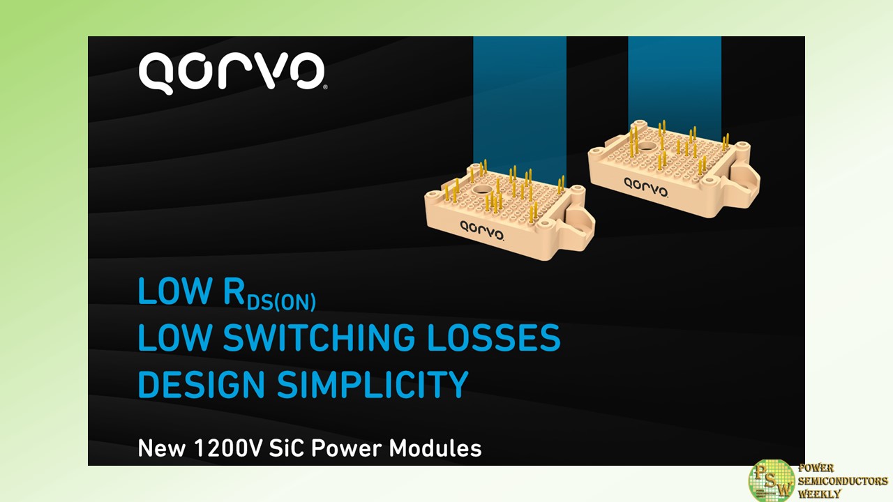
Qorvo® announced four 1200V silicon carbide (SiC) modules – two half-bridge and two full-bridge – in a compact E1B package with RDS(on) starting at 9.4mΩ. These highly efficient SiC modules are excellent solutions for electric vehicle (EV) charging stations, energy storage, industrial power supplies and solar power applications.
“The modules in this new family can replace as many as four discrete SiC FETs, thus simplifying thermomechanical design as well as assembly. Our cascode technology also allows higher switching frequency operation, further reducing solution size by using smaller external components,” said Ramanan Natarajan, director of product line marketing for Qorvo’s SiC Power Products business.
“For our customers, the high efficiency of these modules streamlines the power supply design process, so they can focus on the design, layout, assembly, characterization and qualification of one module as opposed to numerous discrete components.”
Led by the 9.4mΩ UHB100SC12E1BC3N, these four SiC modules leverage Qorvo’s unique cascode configuration, which minimizes RDS(on) and switching losses to maximize efficiency, especially in soft-switching applications. Silver-sinter die attach reduces thermal resistance to as low as 0.23 °C/W; when combined with the stacked die construction found in the “SC” part numbers, power cycling performance is improved by 2X over comparable SiC power modules on the market.
Together, these characteristics contribute to superior thermal performance and reliability with the ease of use and power density of a highly integrated SiC power module.
The table below provides a snapshot of Qorvo’s new 1200V SiC module family:
Part # Description RDS(on) @25C (mΩ) UFB15C12E1BC3N 1200V, 15A SiC full-bridge module 70 UFB25SC12E1BC3N 1200V, 25A SiC full-bridge module 35 UHB50SC12E1BC3N 1200V, 50A SiC half-bridge module 19 UHB100SC12E1BC3N 1200V, 100A SiC half-bridge module 9.4 Qorvo’s suite of powerful design tools like its FET-Jet Calculator and QSPICE™ software aid in product selection and performance simulation. For more information about Qorvo’s advanced SiC solutions for industrial applications, please visit www.qorvo.com/go/sic.
Original – Qorvo
-
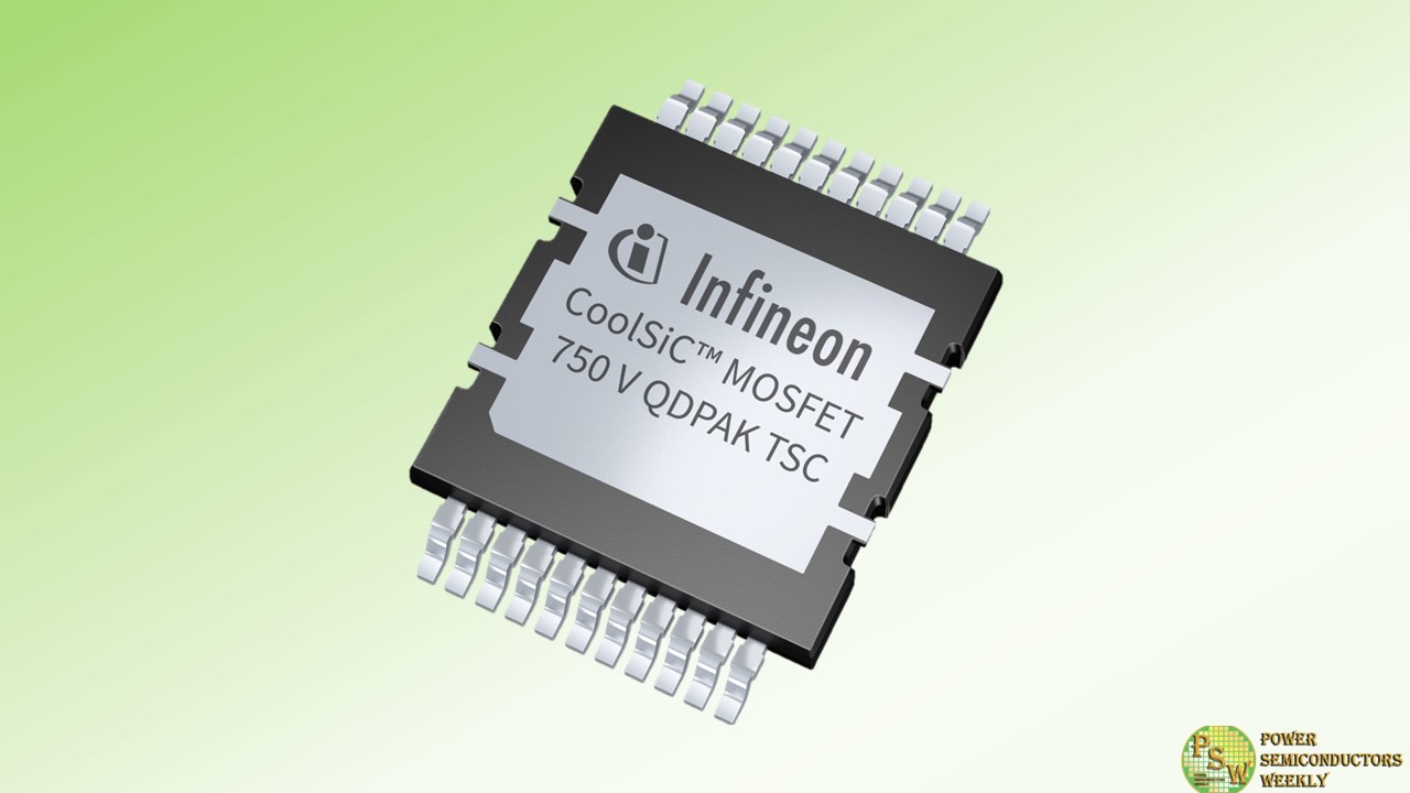
Infineon Technologies AG introduced the 750V G1 discrete CoolSiC™ MOSFET to meet the increasing demand for higher efficiency and power density in industrial and automotive power applications. The product family includes both industrial-graded and automotive-graded SiC MOSFETs that are optimized for totem-pole PFC, T-type, LLC/CLLC, dual active bridge (DAB), HERIC, buck/boost, and phase-shifted full bridge (PSFB) topologies.
The MOSFETs are ideal for use in both typical industrial applications, such as electric vehicle charging, industrial drives, solar and energy storage systems, solid state circuit breaker, UPS systems, servers/ datacenters, telecom, and in the automotive sector, such as onboard chargers (OBC), DC-DC converters, and many more.
The CoolSiC MOSFET 750 V G1 technology features excellent RDS (on) x Q fr and superior RDS (on) x Q oss Figure-of-Merits (FOMs), resulting in ultra-high efficiency in hard-switching and soft-switching topologies respectively. Its unique combination of high threshold voltage (V GS(th), Typ. of 4.3 V) with low Q GD/Q GS ratio ensures high robustness against parasitic turn-on and enables unipolar gate driving, leading to increased power density and low cost of the systems.
All devices use Infineon’s proprietary die-attach technology which delivers outstanding thermal impedance for equivalent die sizes. The highly reliable gate oxide design combined with Infineon’s qualification standards delivers robust and long-term performance.
With a granular portfolio ranging from 8 to 140 mΩ RDS (on) at 25°C, this new CoolSiC MOSFET 750 V G1 product family meets a wide range of needs. Its design ensures lower conduction and switching losses, boosting overall system efficiency.
Its innovative packages minimize thermal resistance, facilitate improved heat dissipation, and optimize in-circuit power loop inductance, thereby resulting in high power density and reduced system costs. It’s important to note that this product family features the cutting-edge QDPAK top-side cooled package.
Original – Infineon Technologies
-

Arrow Electronics, Inc. and its engineering services company, eInfochips, are working with Infineon Technologies AG to help eInfochips’ customers accelerate the development of electric vehicle (EV) chargers.
Development of EV chargers, especially DC “fast chargers,” is becoming increasingly challenging to equipment manufacturers due to several factors, such as lack of prior experience, stringent functional safety and reliability requirements, and a fledgling support network. The collaboration between Arrow and Infineon aims to help innovators navigate these challenges while accelerating time-to-market.
As part of the collaboration, Arrow’s High Power Center of Excellence has developed a 30kW DC fast charger reference platform. This includes Infineon’s 1200V CoolSiC™ Easy power modules and also hardware design, embedded firmware, bi-directional charging support and energy metering functionality.
“Combining Arrow’s strength in components, engineering and design services with Infineon’s innovative products will help customers accelerate their design and speed to market in e-mobility applications,” said Murdoch Fitzgerald, vice president, global engineering and design services at Arrow. “Customers can rely on this collaboration to deliver innovative and leading edge DC faster chargers, accelerate and de-risk design cycles, and get access to a world-class support team enabling them to plan and manage their product roadmap and lifecycles.”
“Infineon is on a drive towards decarbonization and digitalization with our ecosystem partners, and this collaboration with Arrow is a testament to this mission,” said Shri Joshi, vice president of Green Industrial Power, Infineon Technologies Americas. “The joint 30kW DC fast charger reference platform, which includes Infineon’s latest power modules and devices, will help our customers bring more fast chargers to market as the future moves to electrical vehicles. We look forward to this ongoing collaboration to support our customer base.”
The first reference design from this collaboration, a production-grade 30kW DC fast charger reference development platform, is being demonstrated at Applied Power Electronics Conference, Feb. 25-29, in Long Beach, Calif.
Original – Arrow Electronics
-
Vishay Intertechnology, Inc. announced that at the Applied Power Electronics Conference and Exposition (APEC) 2024, the company is showcasing its broad portfolio of passive and semiconductor solutions that address the latest trends in power electronics — from energy harvesting, electric vehicle (EV) powertrains, and mass commercialization to efficient and effective power electronics for power tools and switching regulators that shorten the iterative design cycle.
Taking center stage in booth 1607 will be Vishay’s newly released 1200 V MaxSiC™ series silicon carbide (SiC) MOSFETs, which deliver on-resistances of 40, 80 and 250 mΩ in standard packages for industrial applications, with custom products also available. In addition, Vishay will provide a roadmap for 650 V to 1700 V SiC MOSFETs with on-resistances ranging from 12 mΩ to 1 Ω.
Vishay’s SiC platform is based on a proprietary MOSFET technology — enabled through the company’s recent acquisition of MaxPower Semiconductor, Inc. — which will address market demands in traction inverter, photovoltaic energy storage, on-board charger, and charging station applications. At the booth, Vishay’s experts will also be discussing upcoming planned releases of the MaxSiC platform, including AEC-Q101 Automotive Grade products.
At APEC 2024, Vishay will also be offering a variety of product-focused demonstrations highlighting IHPT haptic actuators; the THJP ThermaWick® Thermal Jumper; the pulse performance of MELF, CRCW / CRCW-HP thick film, and MCS, MCU, and MCW thin film chip resistors; and the thermal capabilities of the PCAN and RCP high power thin and thick film resistors. In addition, application-focused demonstrations will include:
- An 800 V SiC MOSFET heat pump with a 100 % Vishay BOM
- A high voltage intelligent battery shunt for 400 V and 800 V batteries
- A six-phase DC/DC converter for mild hybrid vehicles with 48 V boardnets that provides power to 12 V loads up to 3 kW with high efficiency to 97 %
- A semiconductor-based, resettable eFuse for 800 V electric vehicle systems
Additional Vishay passive components on display at APEC 2024 will include the IHDM series of high current, edge-wound through hole inductors with continuous operation to +180 °C; hybrid planar and integrated transformers; wireless charging coils; NTC thermistors and PTC thermistors, including the PTCEL series capable of handling energy absorption up to 240 J; high power wirewound, thin film, and thick film resistors, including the anti-surge RCS with power to 0.5 W in the 0805 case size; high voltage thick film resistors and dividers; high voltage aluminum, ceramic, and power electronic capacitors (PEC); high energy tantalum capacitors; and robust metallized polypropylene film capacitors, including the MKP1848e DC-Link capacitor with high temperature operation to +125 °C.
Highlighted Vishay semiconductor solutions will consist of the SiC967 high voltage synchronous buck regulator with integrated power MOSFETs and inductors; 400 V, 600 V, and 1200 V standard rectifiers in SlimDPAK 2L and SMPD 2L packages with high creepage distance; 650 V and 1200 V SiC Schottky diodes up to 12 A in eSMP® series and power packages for AC/DC power factor correction (PFC) and ultra high frequency output rectification; and transient voltage suppressors (TVS).
Original – Vishay Intertechnology
-
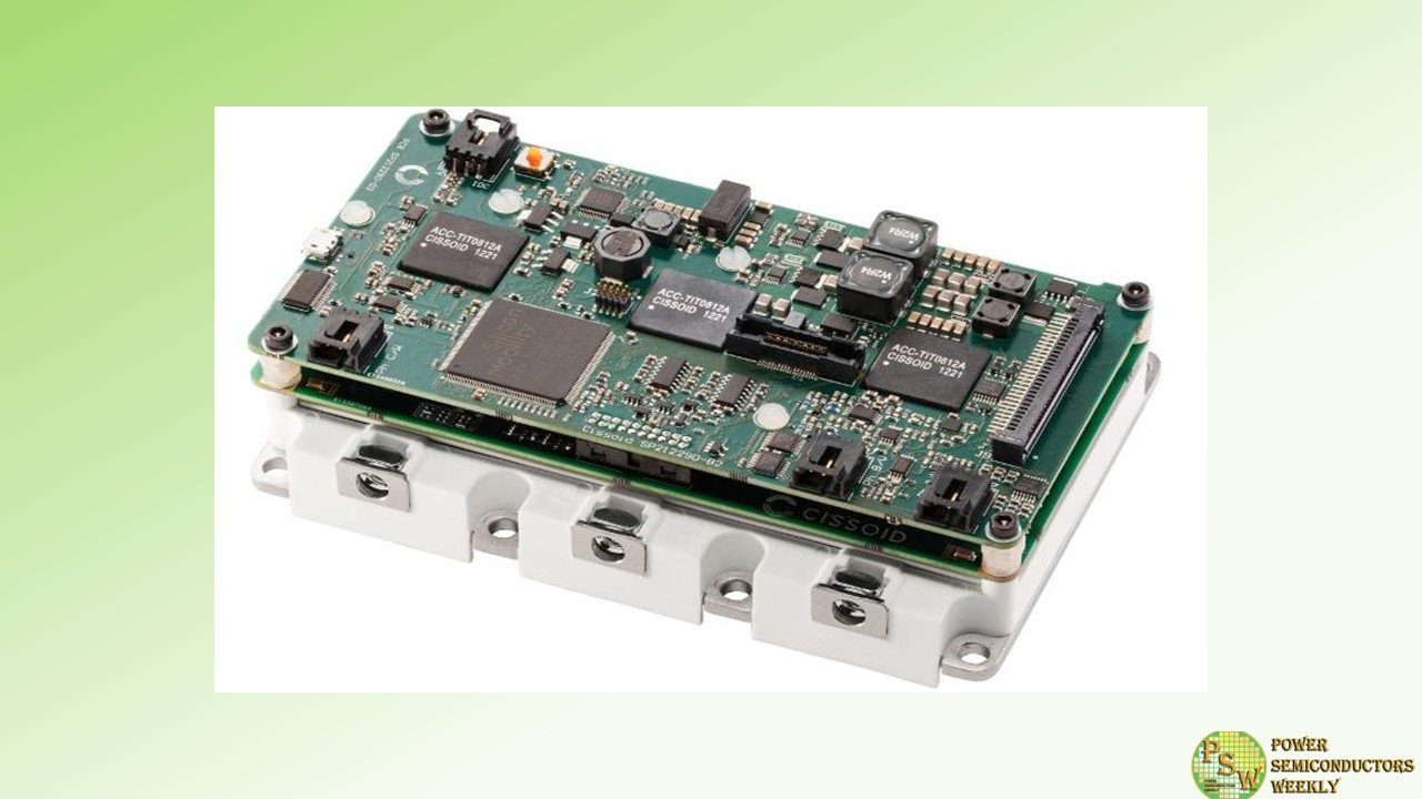
At the Applied Power Electronics Conference (APEC), CISSOID released its new series of SiC Inverter Control Modules (ICMs) dedicated to the E-mobility market. These software-powered SiC Inverter Control Modules are designed to help engineers create functionally safe, robust and modular E-motor drives while dramatically shortening time-to-market.
The new CXT-ICM3SA series offers optimal hardware and software integration of CISSOID’s existing line of 3-phase 1200V/340A-550A SiC MOSFET Intelligent Power Modules (IPMs) with an OLEA® T222 Field Programmable Control Unit (FPCU) control board and OLEA® APP INVERTER application software, supplied in partnership with Silicon Mobility. Depending on the selected ICM product, this modular core engine is capable of powering and controlling high voltage SiC traction inverters with battery voltages up to 850V, at output power exceeding 350kW, and with peak efficiency above 99%.
This unique integration facilitates the rapid development of SiC inverters by solving head-scratching EMC issues often generated due to fast-switching SiC transistors, by supporting different modulation schemes, e.g. SVPWM or DPWM, combined with dead time compensation, and by offering advanced motor control algorithms, including Field Oriented Control (FOC) and Flux Weakening management.
CISSOID further improves time-to-market by providing a complete SiC inverter reference design allowing motor bench testing of the ICM together with key peripheral elements such as current sensors, a high-performance DC-Link capacitor and EMI filter. Both the ICM and the reference design can be obtained from CISSOID, together with the motor control software and on-site technical support.Delivering leadership performance, the ICM supports the drive of high-speed motors, with no compromise on efficiency, thanks to the combination of CISSOID’s low losses SiC power module with the ultra-fast real-time FPCU, enabling high switching frequencies up to 50kHz. Furthermore, this application-specific processor dedicated to e-motor control, with onboard programmable hardware, accelerates the response time to critical events, off-loading the processor cores and enhancing functional safety. Both the FPCU and the control software are ISO-26262 ASIL C/D certified and AUTOSAR 4.3 compliant.
Original – CISSOID
