-
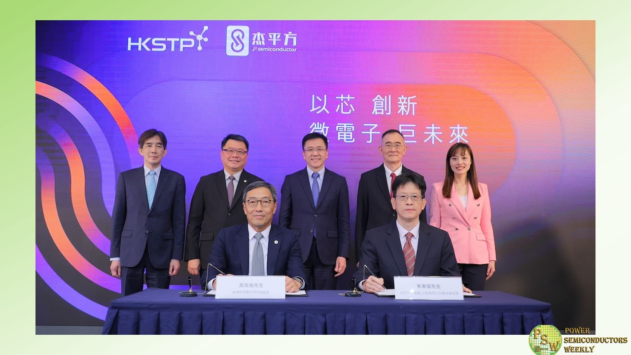
With support from the Innovation, Technology and Industry Bureau and the Office for Attracting Strategic Enterprises (OASES), the Hong Kong Science and Technology Parks Corporation (HKSTP) has signed a Memorandum of Understanding (MoU) with mainland China-based microelectronics enterprise J2 Semiconductor (Shanghai) Co. Ltd. (J2 Semiconductor), to set up a global research and development (R&D) Centre focusing on third-generation semiconductors at the Hong Kong Science Park, and to set up Hong Kong’s first Silicon Carbide (SiC) 8-inch advanced wafer fab.
This is a milestone moment in the government’s ambition to establish Hong Kong as a leading microelectronics hub in the region. This further promotes new industrialisation, a core for the Innovation, Technology and Industry Bureau which published its “Hong Kong Innovation and Technology Development Blueprint”, with a mission to develop strategically advanced manufacturing industries, such as microelectronics and semiconductors. As one of the world’s largest import and export markets for semiconductors, Hong Kong is at the heart of the Greater Bay Area which offers huge potential in becoming a key hub in the global semiconductor supply and value chain.
Professor Sun Dong, Secretary for Innovation, Technology and Industry, said “This collaboration between HKSTP and J2 Semiconductor to set up the Hong Kong’s first-ever large-scale semiconductor wafer fab, demonstrates the commitment of the HKSAR Government in taking the initiative to turn its ‘new industrialisation’ vision into action. J2 Semiconductor is proactively building up the capacity, quality and competitiveness of Hong Kong’s tech talent pool. The project will also drive the development of related industries, including semiconductor equipment manufacturers, material suppliers, testing service providers, to develop a complete ecosystem to reinforce Hong Kong’s position in the global semiconductor industry value chain.”
The collaboration between HKSTP and J2 Semiconductor is jointly supported by the Innovation, Technology and Industry Bureau and OASES with a view to sustain Hong Kong’s innovation and technology ecosystem and promote new industrialisation. The MoU was witnessed by Professor Sun Dong, Secretary of Innovation, Technology and Industry Bureau, Mr Philip Yung, Director-General of OASES, Ms Lillian Cheong, Under Secretary for Innovation, Technology and Industry, Dr Sunny Chai, Chairman of HKSTP and Dr Robert Tsu, Chairman of J2 Semiconductor. While Mr Albert Wong, CEO of HKSTP and Mr TY Chu, Co-CEO of J2 Semiconductor formally signed the MoU.
Dr Sunny Chai, Chairman of HKSTP said, “The plan of establishing J2 Semiconductor’s R&D Centre in the Science Park will promote Hong Kong’s R&D and advanced manufacturing capabilities of third-generation semiconductor devices. J2 Semiconductor brings the core technology and expertise to Hong Kong in advanced chip design, fabrication process and semiconductor product development, which is an important milestone in the development of microelectronics industry in Hong Kong. As one of Hong Kong’s flagship innovation and technology platforms, we provide high-quality infrastructure and facilities as well as a vast network of partners, which will continue to promote Hong Kong’s microelectronics R&D capabilities and strengthen Hong Kong’s position as an international I&T hub.”
Dr Robert Tsu, Chairman of J2 Semiconductor said, “I am very grateful for the level of attention and support from both the Innovation, Technology and Industry Bureau and HKSTP to this project. The MoU signing officially launches our third-generation semiconductor ‘SiC 8-inch advanced wafer fab’ project. J2 Semiconductor will invest an estimated HK$6.9 billion into the project, with plans to start volume production in the next couple of years, and reach annual production capacity of 240,000 SiC wafers in 2028, generating an annual production value of more than HK$11 billion and creating more than 700 job positions in Hong Kong. The project will assist in the early completion of the localisation of the new energy vehicle supply chain and drive the long-term development and prosperity of the semiconductor industry in Hong Kong.”
As a semiconductor chip design enterprise, J2 Semiconductor is committed to meeting the strong demand for domestically produced automotive chips from the China automotive industry. It mainly provides high-performance silicon carbide (SiC) devices with a focus on automotive, power conversion and communications. J2 Semiconductor’s superior SiC technology can be applied to relevant applications such as electric vehicles, as well as the related infrastructure such as charging stations, smart grids and energy storage.
HKSTP is committed to promoting Hong Kong’s new industrialisation mission and building a world-leading microelectronics ecosystem. HKSTP has established an extensive network of microelectronics hardware infrastructure, including Sensor Packaging and Integration Laboratory (Sensor Lab), Heterogenous Integration Lab (HI Lab) and the Hardware Lab, which can support the end-to-end process of design, prototyping and pilot production of chip-related equipment and systems as well as products. The Microelectronics Centre in Yuen Long Innovation Park is set to begin operation in 2024, supporting HKSTP’s infrastructure to accelerate microelectronics R&D pilot production, creating opportunities for upstream and downstream enterprises in the industry chain.
The microelectronics ecosystem of HKSTP is flourishing, with more than 200 microelectronics related companies. The establishment of the J2 Semiconductor facilities in Hong Kong will create greater level of synergy and knowledge exchange. Currently, five universities in Hong Kong are ranked among the top 100 universities in the world, with more than 100 university researchers engaged in microelectronics research, and promote the R&D of third-generation semiconductors. In this year’s Budget Speech, the HKSAR Government announced its plan to establish a Microelectronics Research and Development Institute to strengthen collaboration with universities, R&D centres and companies in the industry, and further accelerate the “1 to N” translation of R&D outcomes and bolster industry development.
Original – HKSTP
-
With decades of expertise in power device packaging and testing, JCET Group offers a comprehensive power product portfolio encompassing IGBT, SiC, GaN, and more. In the field of high-density power solutions for automotive applications, JCET’s unique power module technology positions us at the forefront of power main drive solutions.
JCET’s innovative packaging technology for high power density Silicon Carbide (SiC) power modules minimizes parasitic effects and thermal resistance, while our groundbreaking interconnect technology ensures high reliability. Reduced power loss and improved performance, making JCET the preferred choice for high-reliability SiC device packaging for the automotive industry.
The rapid growth of the power semiconductor market in automotive applications is being driven by the acceleration of vehicle electrification. In this evolving landscape, a multitude of power devices find applications in crucial automotive systems such as motor control, DC-DC conversion, air conditioning drives, on-board chargers (OBC), and battery management for electrical vehicles.
According to research by Strategy Analytics, the value of power devices in battery electric vehicles (BEVs) is nearly five times that in traditional fuel vehicles. This is where SiC devices come into play, offering several advantages. SiC devices feature smaller conductor resistors per unit area, higher voltage capabilities, faster switching speeds, and the ability to operate at high temperatures. These characteristics are instrumental in enhancing the power density of the inverter, ultimately leading to improved operational efficiency and extended mileage for electric vehicles under real-world conditions.
JCET combines low stray inductance package technology, advanced interconnect packaging technology, and cutting-edge thermal management solutions, tailoring our packaging processes to meet individual customer requirements. Within this package, a suite of integrated solutions, including the whole-silver sintering process, copper wire bonding, and single-side direct water cooling, is employed.
Furthermore, SiC devices, with their smaller footprint, increased power density, and higher breakdown voltage compared to conventional silicon-based power devices, are at the core of our packaging. When integrated into an 800V platform, SiC devices deliver substantial system advantages, enabling rapid charging and extended mileage. JCET’s unwavering commitment to optimizing packaging technology is evident in our High-Performance Device (HPD) package, which is continuously fine-tuned to excel in SiC high-frequency switching applications.
With the growing adoption of SiC devices across diverse sectors like automotive controllers, charging stations, and photovoltaic energy storage, JCET has pioneered innovative designs encompassing packaging materials, internal connections, and packaging structures. JCET has introduced a range of packaging solutions tailored to meet various user requirements, including:
- 400V platform, A0/A00 vehicles within 70KW: Si Hybrid Package1 solution;
- 400V platform, Class A vehicles between 100-200KW: Si/SiC Hybrid Package Driver solution;
- 800V platform, Class B and luxury cars with 200KW and above: SiC single/double sided heat dissipation solution.
Automotive power devices, including SiC, hold vast market potential and exhibit a high level of technical innovation certainty. This presents a compelling opportunity for device designers and manufacturers. Looking ahead, JCET remains committed to its core mission of advancing power device packaging solutions, We are dedicated to expanding our technology offerings, ensuring our customers have a diverse array of options, helping them integrate more efficient and reliable technologies into the new energy vehicle systems.
Original – JCET
-
Mitsubishi Electric Corporation has agreed with Coherent Corp. to invest USD 500 million in a new silicon carbide (SiC) business to be carved out from Coherent, aiming to expand its SiC power device business by strengthening vertical collaboration with Coherent, who has been a supplier of SiC substrates to Mitsubishi Electric.
The electric vehicle market is expanding worldwide and is one of several emerging applications driving the exponential growth of SiC power devices, which offer lower energy loss, higher operating temperatures and faster switching speeds than conventional silicon power devices. The high efficiency of SiC power devices is expected to contribute significantly to global decarbonization and green transformation.
Mitsubishi Electric has been a leader in SiC power modules for high-speed trains, high-voltage industrial applications, and home appliances for many years. The company made history by launching the world’s first SiC power modules for air conditioners in 2010, and became the first supplier of a full SiC power module for Shinkansen high-speed trains in 2015. Mitsubishi Electric has also accumulated extensive expertise by meeting market needs for advanced performance and high reliability by deploying superior processing, screening, etc. for the development and manufacture of SiC power modules.
Mitsubishi Electric has been procuring high-quality 150mm SiC substrates from Coherent for the production of SiC power modules for many years. In addition to developing high-quality 200mm SiC substrates with Coherent, Mitsubishi Electric plans to invest approximately 100 billion yen to construct a new 200mm SiC wafer plant in Kumamoto Prefecture, Japan beginning in 2026.
By further deepening its collaboration with Coherent through this investment, Mitsubishi Electric aims to stabilize its procurement of SiC substrates for SiC power modules, for which demand is forecasted to grow rapidly, and thereby expand its supply of reliable high-performance SiC power devices to meet rising global demand.
Dr. Masayoshi Takemi, Executive Officer, Group President, Semiconductor & Device of Mitsubishi Electric, said: “Demand for SiC power semiconductors is expected to grow exponentially as the global market for electric vehicles increases in line with the transition to a decarbonized world. To capitalize on this trend, we have decided to expand our SiC power semiconductor production capacity, including by constructing a 200mm wafer plant in the Shisui area of Kumamoto Prefecture. We are delighted to strengthen our partnership with Coherent by investing in this new SiC company, which will provide us with a stable supply of high-quality SiC substrates essential for our increased supply capacity.”
Original – Mitsubishi Electric
-

DENSO CORPORATION announced a minority investment of US$500 million in Silicon Carbide LLC, Coherent Corp.’s silicon carbide (SiC) business, which will be separated into an independent subsidiary. Silicon Carbide LLC, which was originally established by Coherent in April 2023, manufactures SiC wafers. This investment will ensure a long-term stable procurement of SiC wafers to enhance the competitiveness of our electrification components. With this equity investment, DENSO will hold 12.5% equity stake in Silicon Carbide LLC.
As vehicle electrification accelerates as part of the global effort to reduce CO2 emissions, semiconductor demand has also grown rapidly. SiC is a key material for devices that significantly contribute to reducing power loss, downsizing, and lightweighting of Battery Electric Vehicle (BEV) systems, owing to its superior performance in high-temperature, high-frequency and high-voltage environments compared to that of conventional silicon.
Through this investment in Silicon Carbide LLC, which has an excellent track record in SiC wafer quality and mass production capabilities, DENSO will secure a stable procurement of quality 150mm and 200mm SiC wafers. This will further strengthen the competitiveness of DENSO’s inverters, which drive and control motors of electric vehicles.
“We are very pleased to establish a strategic relationship with Coherent, which has a world-class track record in SiC wafer manufacturing. Through this investment, we will secure a stable procurement of SiC wafers, which are critical for BEVs, and contribute to the realization of a carbon-neutral society by promoting the widespread adoption of BEVs,” said Shinnosuke Hayashi, President & COO, Representative Member of the Board at DENSO.
Dr. Vincent D. Mattera, Jr., Chair and CEO at Coherent, said, “We are excited to expand our strategic relationships with DENSO to capitalize on the significant demand for silicon carbide. After a thorough review of strategic alternatives for our Silicon Carbide business, we determined that the creation of a separate subsidiary and the strategic investments from DENSO, a leader in SiC power devices and modules, is the best path forward to maximize shareholder value and position the Business for long-term growth.
The investments from our strategic partners will be used to accelerate our capacity expansion plans and help sustain our leadership position, while ensuring the development of a robust and scalable supply for the rapidly growing market for SiC-based power electronics, largely driven by the explosive growth of the global electric vehicle market.”
DENSO will continue to contribute to the realization of a carbon-neutral society by promoting the widespread adoption of electrified products in all regions around the world.
Original – DENSO
-
Aehr Test Systems announced financial results for its first quarter of fiscal 2024 ended August 31, 2023.
Fiscal First Quarter Financial Results:
- Net revenue was $20.6 million, up 93% from $10.7 million in the first quarter of fiscal 2023.
- GAAP net income was $4.7 million, or $0.16 per diluted share, up from GAAP net income of $589,000, or $0.02 per diluted share, in the first quarter of fiscal 2023.
- Non-GAAP net income, which excludes the impact of stock-based compensation, was $5.2 million, or $0.18 per diluted share, compared to non-GAAP net income of $1.3 million, or $0.05 per diluted share, in the first quarter of fiscal 2023.
- Bookings were $18.4 million for the quarter.
- Backlog as of August 31, 2023 was $22.3 million. Effective backlog, which includes all orders received since the end of the first quarter, is $24.0 million.
- Cash provided by operations was $3.9 million.
- Total cash, cash equivalents, and short-term investments as of August 31, 2023 were $51.0 million, up from $47.9 million at May 31, 2023.
Gayn Erickson, President and CEO of Aehr Test Systems, commented:
“We finished the first quarter with solid revenue and non-GAAP net income, the strongest first quarter in our history, which has historically been our seasonally softest quarter. We are off to a very good start to our fiscal year and are reaffirming our expectation to grow fiscal full year revenue by at least 50% and profit by over 90% year over year.
“During the quarter we had record shipments of our FOXTM WaferPak full wafer Contactors in both revenue and units and are very pleased with the continued stream of new designs we are seeing. Our new design volume has tripled over the last nine months as we are seeing more electric vehicles coming online with their own specific device design for inverters and onboard chargers.
“We have now received customer acceptance of both configurations of our new fully automated FOX WaferPak Aligner, which allows hands free operation of WaferPak handling and alignment and is available either as a standalone unit or in full integration with the FOX-XP system. We recognized revenue for two standalone WaferPak Aligners in the first quarter and received customer acceptance and sign off on two fully integrated WaferPak Aligners with the integrated FOX-XPs in September. These acceptances and the associated revenue recognition are a great way to start our second quarter and pave the path for revenue recognition immediately upon future shipments of these products.
“Additionally, we announced last month our sixth customer for silicon carbide wafer level burn-in. This new customer is a US-based multibillion-dollar semiconductor supplier that serves several markets, including automotive, computing, consumer, energy, industrial, and medical markets. After conducting a detailed financial evaluation of Aehr and Aehr’s FOX family of products, including multiple onsite visits to Aehr’s application lab, this new customer purchased an initial FOX-NP system, WaferPak Aligner, and multiple WaferPaks for engineering, qualification, and small lot production of their silicon carbide power devices.
This system is configured with our new Bipolar Voltage Channel Module (BVCM) and Very High Voltage Channel Module (VHVCM) options that enable new advanced test and burn-in capabilities for silicon carbide power semiconductors. This customer has indicated that as their production capacity increases, they intend to quickly move to our FOX-XP multi-wafer test and burn-in systems for high-volume production.
“Including this newest customer, our last two announced customers have selected our systems primarily for applications other than electric vehicles including industrial, solar, and commuter electric trains. This further extends our application space beyond the opportunity we see in silicon carbide for traction inverters and onboard and offboard chargers for electric vehicles. These applications expand our market opportunity to include what William Blair forecasts will be an additional 2.8 million 6” equivalent wafers needed per year by 2030 for applications beyond the 4.5 million 6” equivalent wafers per year it forecasts will be needed just for electric vehicles.
“We continue to see increased interest from prospective new customers for our solutions for silicon carbide wafer level burn-in. In the last few weeks, we have attended two international conferences in Europe and met with more than a dozen companies that are not currently using our solutions, in addition to meeting with all six of our current silicon carbide customers. These face-to-face meetings included multiple meetings with one of the market leaders in silicon carbide with whom we have been doing a significant automotive qualification of wafer level burn-in for well over two years.
This benchmark and qualification process has made even more progress in the last few months with a very large number of wafers being run at our facility and multiple meetings and reviews of the data. We continue to feel confident that this customer will move forward with us using the FOX-XP multi-wafer solution for their high-volume needs, including initial purchase orders and system shipments within this fiscal year. In the next few weeks, we also plan to meet with a significant number of potential new customers as well as end users in Asia, as we are seeing increasing activities and opportunities heating up there. It is a very exciting time in the silicon carbide and electric vehicle markets right now and we have never been busier.
“We are also in extensive engagements with multiple gallium nitride suppliers, including companies that also supply silicon carbide devices. Gallium nitride is similar to silicon carbide in that both of these semiconductor compounds are considered wide bandgap semiconductors that are able to withstand high-voltage applications more directly than silicon. Gallium nitride semiconductor material has characteristics that make it optimal for lower power converter applications such as consumer power converters, solar micro inverters, and industrial motor controllers, compared with silicon carbide that is optimal for higher power / higher voltage applications such as traction inverters in electric vehicles, trucks, trains, and converters used in charging infrastructure and storage.
The gallium nitride market is another potential growth driver for our wafer level solutions, particularly for automotive and photovoltaic applications where burn-in appears to be critical for meeting the initial quality and reliability needs of those markets. This fiscal year, while we do expect to recognize some revenue for systems, WaferPaks and Aligners for gallium nitride applications, we continue to expect a significant majority of our revenue to come from silicon carbide.
“In addition to these power semiconductor applications, we continue to be excited about the current application of silicon photonics devices for fiber optic transceivers used in data centers and data and telecommunication networks, as well as the major market opportunity we see with the upcoming application of silicon photonics integrated circuits for use in optical chip-to-chip communication. As we’ve previously announced, we received a first order from a current major silicon photonics customer for a new configuration of our FOX-XP multi-wafer test and burn-in system for use in very high-power silicon devices, and we expect to receive orders for additional production systems as they increase production of these devices.
While we believe that it will likely be several years before we will potentially see significant revenue generated from this optical chip-to-chip communications market, we are working with some of the leaders in silicon photonics to ensure that we have the products and solutions available to meet their needs for this potentially significant market application.
“In conclusion, we are encouraged by the continued positive momentum we are seeing for silicon carbide in electric vehicles and are also excited about the expanding growth opportunities we are seeing in several additional markets with current and prospective customers.”
Original – Aehr Test Systems
-

Revasum, Inc. announced a strategic partnership with SGSS, a global leader in high-performance materials and innovative solutions. This partnership aims to revolutionize the semiconductor industry by developing a cutting-edge line of grinding wheels specifically designed for Silicon Carbide (SiC) wafers.
Silicon Carbide is a critical material in the production of power devices and has gained significant prominence in the semiconductor industry due to its exceptional properties. The demand for SiC wafers has been steadily growing, and achieving the highest quality wafers is paramount to meet the evolving needs of the market.
The partnership between Revasum and SGSS represents a collaboration between two industry giants with a shared commitment to innovation and excellence. By combining Revasum’s expertise in semiconductor manufacturing equipment with SGSS’s cutting-edge abrasive materials, this alliance seeks to develop a new generation of surface finishing solutions that will set new standards for precision, efficiency, and surface quality in SiC wafer production with sustainability and environmental responsibility at the core of our collaboration.
This partnership holds great promise for the semiconductor industry, paving the way for enhanced SiC wafer production processes that will contribute to the advancement of power electronics, electric vehicles, renewable energy, and various other technology sectors.
Mr. Scott Jewler, CEO of Revasum, Inc., commented on the partnership, saying, “We are excited to join forces with Saint-Gobain Surface Solutions, a renowned leader in materials science and innovation. This partnership will enable us to provide our customers with cutting-edge tools and solutions to address the increasing demand for high-quality Silicon Carbide wafers.”
Mr. Jean-Claude Lasserre, CEO Saint-Gobain Surface Solutions stated, “Our collaboration with Revasum exemplifies our commitment to delivering high-performance materials and solutions that push the boundaries of what is possible. Together, we will unlock new levels of precision and efficiency in Silicon Carbide wafer grinding with highest levels of sustainable products and solutions.”
Both Revasum, Inc. and SGSS are eager to embark on this journey of innovation and look forward to delivering groundbreaking solutions that will shape the future of Silicon Carbide wafer manufacturing.
Original – Revasum
-
Solitron Devices has acquired Micro Engineering Inc. located in Apopka, FL. Specializing in highly integrated, high reliability assemblies, Micro Engineering has over forty years of experience servicing medical, industrial, and aerospace applications.
Focused on low to mid volume production, Micro Engineering offers services from conceptual design and prototyping to full turnkey manufacturing and functionally tested assemblies. Additional services include hand assembly, wire harnessing, specialized coatings and full box builds.
Mark Matson, Solitron President & COO, said, “Micro Engineering is an exceptionally synergistic fit with Solitron, expanding and complimenting engineering and manufacturing capabilities. Solitron’s expertise with chip and wire, silicon carbide and high-density multi-chip modules combined with Micro Engineering’s PCBA, SMT and system level box build capability offers a strong suite of technology to customers.
This new capability for increased functionality and power density will accelerate introductions into emerging markets particularly utilizing Silicon Carbide (SiC) and Gallium Nitride (GaN). The combination of Solitron and Micro Engineering will also broaden both companies’ presence in medical, high end industrial and aerospace applications.”
Combined manufacturing capabilities now include 3D CAD modelling, 3D Printing, CAE machining, aluminum & gold wire bonding, void free soldering, fine pitch SMT for BGA’s, rigid, flex and double-sided circuit card assemblies; right up through full box builds. Product qualification infrastructure includes thermal shock, vibration, mechanical shock, centrifuge, salt spray atmosphere, burn-in and more. Micro engineering is ISO-9001 registered.
Original – Solitron Devices
-
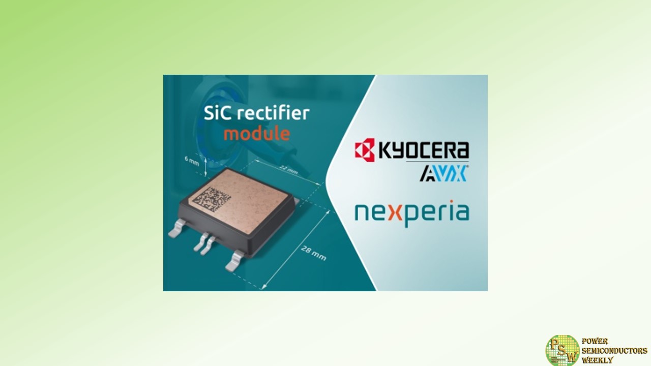
Nexperia has entered into partnership with KYOCERA AVX Components (Salzburg) GmbH to jointly produce a new 650 V, 20 A silicon carbide (SiC) rectifier module for high frequency power applications ranging from 3 kW to 11 kW power stack designs, aimed at application like industrial power supplies, EV charging stations, and on-board chargers. This release will represent a further deepening of the existing, long-lasting partnership between the two companies.
Space-saving and weight reduction are the key requirements for manufacturers of the next generation power applications. The compact footprint of this new SiC rectifier module will help to maximize power density, thereby reducing the amount of required board space and lowering the overall system cost.
Thermal performance is optimized using a combination of top-side cooling (TSC) and an integrated negative temperature coefficient (NTC) sensor which monitors the device temperature and provides real time feedback for device or system level prognosis and diagnosis. This rectifier module has a low inductance package to enable high frequency operation and it has been qualified to operate with a junction temperature of up to 175 °C.
“This collaboration between Nexperia and KYOCERA AVX combines cutting edge silicon carbide semiconductors with state-of-the-art module packaging and will allow Nexperia to better serve the market demand for power electronic products which offer exceptionally high levels of power density,” according to Katrin Feurle, Senior Director of the Product Group SiC at Nexperia. “The release of this rectifier module will represent the first step in what is envisaged as a long-term SiC partnership between Nexperia and KYOCERA AVX”.
Thomas Rinschede, Deputy Vice President Sensing and Control Division at KYOCERA AVX Components Sensing and Control Division, comments: “We are delighted to further extend our successful partnership with Nexperia into the production of silicon carbide modules for power electronics applications. Nexperia’s manufacturing expertise combined with KYOCERA module know-how make a compelling offering for customers looking to achieve higher power densities using wide bandgap semiconductor technology.”
Nexperia expects samples of the new SiC rectifier modules to be available in the first quarter of 2024.
Original – Nexperia
-

Yield Engineering Systems, Inc. (YES), a leading manufacturer of process equipment for semiconductor, life sciences, and “More-than-Moore” applications, had sold multiple Wet Processing Systems to a premier Silicon Carbide (SiC) materials manufacturer. The adoption of SiC Wide Band Gap (WBG) semiconductors continues to grow with demand driven by Electric Vehicle (EV) production and charging infrastructure, power supply systems, and Photovoltaic (PV) inverters.
The YES TersOnus™ wet solution continues to gain momentum in the SiC market. YES’ highly flexible and custom-configured systems have superior temperature uniformity complimented by ultra-low particle performance. These systems can address 150mm and 200mm Silicon Carbide processes without process downtime or line changes.
“Silicon carbide materials manufacturers are seeking technology partners that provide specific solutions to their roadmap challenges. TersOnus™ for post epitaxial & chemical mechanical polishing (CMP) wet cleaning addresses these specific needs by providing unparalleled process efficacy, automated handling capabilities, and adaptable system configurations with significant Cost of Ownership advantages. This multi-tool order validates YES’ efforts to serve our SiC customers and allow them to go to market quickly with proven HVM solutions.” said Dragan Cekic, VP of Strategic Sales for YES,
“YES has a rich history of providing highly automated, customer-configured wet processing technology. YES is excited about our involvement in the rapidly growing global market for SiC devices. This order confirms our solutions’ value proposition for the broader SiC ecosystem,” said Kevin Trompak, Vice President of Business Development for YES. “YES is committed to supporting the development of SiC solutions by investing in an Advanced Technology Center in Chandler, Arizona, which officially opened July 27th this year.”
Original – Yield Engineering Systems
-
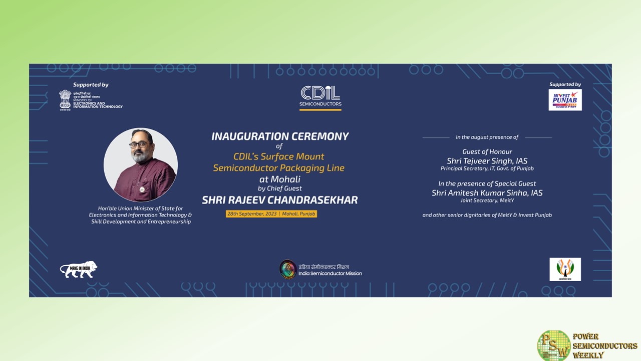
Hon’ble Union Minister of State for Electronics and Information Technology, Shri Rajeev Chandrasekhar, virtually inaugurated the new Surface Mount Semiconductor Packaging Line, at Continental Device India Private Limited’s (CDIL) Mohali plant today. With the new versatile SMA and SMB package line, via the Government of India’s SPECS, CDIL becomes India’s first Silicon Carbide components manufacturer, scaled to make auto-grade devices, including Silicon Carbide MOSFETs, Silicon Carbide Schottky Diodes, Rectifiers, Zeners and TVS Diodes among others for the global as well as the domestic market. The expansion of assembly lines will increase CDIL’s total capacity at the facility to 600 million units annually.
The new line inauguration was also attended by Shri Tejveer Singh, IAS, Principal Secretary, IT, Government of Punjab, and Shri Amitesh Kumar Sinha, IRAS, Joint Secretary, MeitY and other senior dignitaries of MeitY and Invest Punjab.
With the impending surge in electric vehicles (EVs), power management devices and solar-powered panels, globally as well as in India, and their increased reliance on wide band gap electronics, CDIL identified and laid focus on Silicon Carbide (SiC) products.
SiC is an emerging technology that allows for much-improved efficiencies and power-handling capabilities, especially in high-power charging applications and battery management systems. CDIL spent R&D efforts pursuing SiC technology so as to build proficiency and assist in the world’s switch to Electric Vehicles.
Expressing his gratitude, Tejveer Singh, IAS, Principal Secretary, IT, Government of Punjab, said, “I am very very thankful to the CDIL team for this great effort in expanding the plant capacity and assembly line. And as CDIL and SCL sign the MoU, we can finally see Mohali becoming the chip-making hub of India. The Government has a vision to cultivate a dynamic semiconductor ecosystem in Mohali and therefore, the modernization of SCL could provide the sector the much needed impetus to put Mohali on the semiconductor manufacturing map of India.”
Speaking at the launch of the new assembly lines, Amitesh Kumar Sinha, IRAS, Joint Secretary, MeitY, said, “India’s Semiconductor mission is a key focus for both the Union and the State Governments, and there have been many developments in the sector. Yet, India still has much to catch up, with a projected surge in demand to approximately $110 billion by 2030. At MeitY, our objective is to modernise and commercialise SCL with focus on making it a R&D hub for developing the semiconductor ecosystem in the country.
It’s heartening to see CDIL taking the lead in Packaging of discrete semiconductor devices. CDIL has capability for R&D, Design, and Packaging. Earlier, they also had a fabrication facility. I hope CDIL will also consider setting up a discrete fab in the country by availing financial support under the Semicon India programme in future. As CDIL and SCL join hands for knowledge exchange, India can look forward to more indigenous chip manufacturing and packaging for India and the world in the upcoming future.”
CDIL has also established an advanced testing and reliability laboratory at the Mohali plant. The facility, a one-of-a-kind in India, is equipped to meticulously qualify the semiconductor products according to the stringent standards stipulated by the Automotive Electronics Council (AEC), ensuring they meet the rigorous demands of the automotive domain.
Commenting on the same, Prithvideep Singh, General Manager, CDIL said, “In line with our steadfast commitment to innovation and market diversification, CDIL Semiconductors has strategically positioned itself to meet the burgeoning demands of the automotive sector, both within India and on a global scale. Even though SiC devices are notoriously hard to manufacture at scale, we have spent effort and investment to master them. CDIL has been able to innovate on the brittleness and complexity around the production of SiC devices and has earned the resounding approval of large multinational customers in export markets.”
CDIL also signed an MoU with the Semi-Conductor Laboratory (SCL), a research institute in Mohali under MeitY, undertaking research and development in the field of semiconductor technology. Both parties will aim to establish a comprehensive framework wherein SCL’s specialized knowledge and wafer fabrication facilities are utilized to produce indigenized wafers for CDIL’s discrete semiconductor devices, using CDIL’s proprietary manufacturing processes. This collaborative effort is aimed as a significant stride towards advancing India’s semiconductor ambitions in fostering a stronger, self-reliant industry in the region.
Silicon Carbide (SiC) material boasts a significantly wider bandgap compared to traditional semiconductor materials like silicon. A wide bandgap (~3.26 eV for SiC) enables SiC devices to operate at higher temperatures and handle higher breakdown voltages. Consequently, SiC emerges as the optimal choice for the electric vehicle (EV), power management and solar sectors, as it allows semiconductor components to operate reliably in high temperatures, reducing the need for complex cooling systems.
The company has already initiated pilot production in August with 50 million units and promptly delivered its inaugural batch to customers in both the domestic and international markets. CDIL operates manufacturing facilities and a reliability lab in Mohali and Delhi, serving industries with a strong emphasis on the Automotive, Defence, and Aerospace sectors. With 59 years of legacy, a worldwide customer base, with many industry leaders as loyal customers spread throughout the world including China, Brazil, Germany, Hong Kong, Japan, Malaysia, Russia, Singapore, South Africa, South Korea, Turkey, USA and the UK.
Original – CDIL Semiconductors
