-
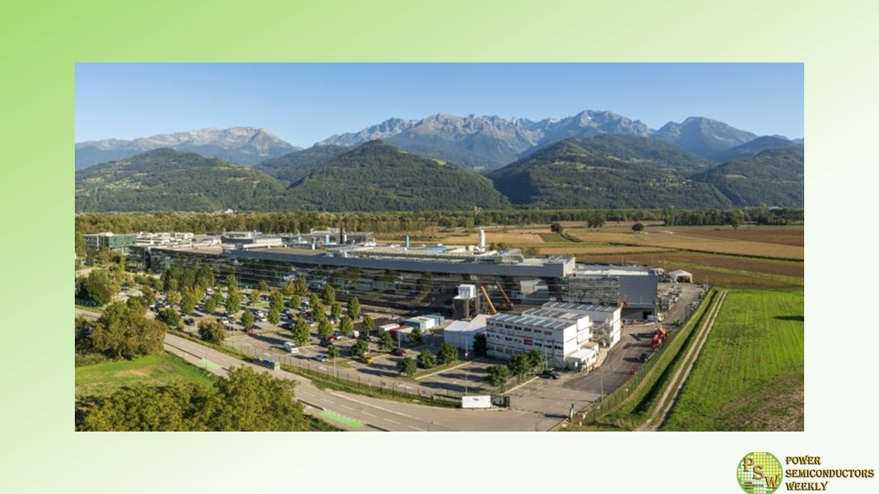
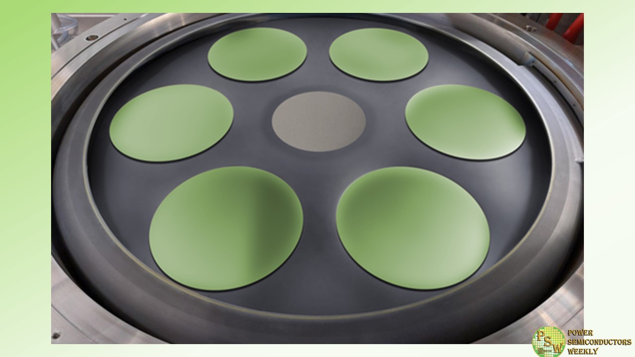
Soitec opened its new plant in Bernin, near Grenoble, in the presence of Thierry Breton, European Commissioner for the Internal Market and Roland Lescure, French Minister Delegate for Industry.
Soitec has developed its SmartSiC™ technology as a response to vehicle electrification challenges.
The technology, based on silicon carbide (SiC), sets a new standard with improved efficiency for energy conversion systems. Thanks to its reduced energy losses, better thermal management and improved power density, the material increases the range and performance of electric vehicles.
Through the application of SmartCut™ technology, each SiC substrate can be used 10 times.
As a result, SmartSiC™ enables electric vehicles to achieve ranges above 500 km, compared with an average 350 km for vehicles using silicon IGBT alternatives – while also reducing CO2 emissions during wafer manufacturing by 70% compared to monocrystalline SiC substrates.
Development of the technology began in 2020 in partnership with CEA-Leti and has received financial support from the French state, the region, local authorities and the European Union.
A new production facility in step with Soitec’s ambition
The new plant will have a 2,500 m2 footprint and a final production capacity of 500,000 SmartSiC™ wafers per year.
It will contribute to Soitec’s strategy of sustainable growth towards a threefold expansion of addressable markets by 2030, reinforcing the company’s leadership position in the strategic semiconductor materials market.
The new plant will lead to the creation of 400 direct jobs, while also reinforcing the attractiveness and dynamism of the “French Silicon Valley” ecosystem.
Pierre Barnabé, Chief Executive Officer of Soitec, stated: “More than ever we are ready to establish our SmartSiC™ technology as a new standard in semiconductor materials for coming generations of electric cars. This plant will enable us to meet growing demand for silicon carbide and achieve a 30% market share by 2030, while helping to make electric mobility more efficient and affordable. Completed in record time, it is the embodiment of our industrial performance and our future-facing strategy, based on the expansion of our product and technology portfolio.
This is also an important day for our region, which is once again showing its dynamic and exemplary approach to industrial innovation, with technologies designed, developed, and manufactured within our ecosystem. We will create jobs and continue to showcase French and European knowhow in global semiconductor markets.”
Original – Soitec
-
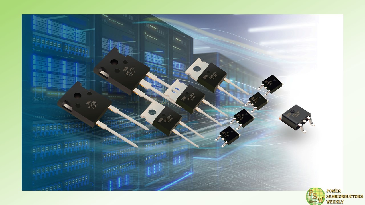
Bourns, Inc. has expanded its 650 and 1200 V Silicon Carbide (SiC) Schottky Barrier Diode (SBD) product family with 10 new models. The 10 new models added to the Bourns® SiC SBD line are designed to address the increasing power density requirements in the latest transportation, renewable energy and industrial systems.
Bourns’ expanded wide band gap diode line delivers the peak forward surge, low forward drop, reduced thermal resistance and low power loss capabilities demanded by today’s high frequency and high current applications. These capabilities also help designers develop smaller, cost-efficient and state-of-the-art power electronics.
As optimal power conversion solutions for DC-DC and AC-DC converters, Switched-Mode Power Supplies (SMPS), photovoltaic inverters, motor drives and other rectification applications, the 10 new models feature currents in the 5-10 A range, with no reverse recovery current to reduce EMI.
This enables them to significantly lower energy losses and further increase efficiency, switching performance and reliability. In addition to providing excellent thermal performance, Bourns’ new SiC SBD models are available in multiple forward voltage, current and package options that include TO220-2, TO247-3, TO252, TO263 and TO247-2.
The 10 new Bourns® BSD SiC SBD models are available now. These models are RoHS compliant, halogen free, Pb free and their epoxy potting compound is flame retardant to the UL 94V-0 standard. For more detailed product information, please see: www.bourns.com/products/diodes/silicon-carbide-sic-schottky-barrier-diodes.
Original – Bourns
-
During the past decade combination “silicon carbide” or more often “SiC” has become very popular in the world of power electronics. Many companies have started to evaluate the possibility of using SiC instead of Si in their projects. As many say, silicon carbide is here to replace silicon, and they might be right considering that SiC MOSFETs used in power semiconductor devices bring numerous advantages compared with their silicon counterparts.
SiC has a higher critical breakdown field and thermal conductivity and, a wider bandgap, which leads to lower energy losses, a lower leakage current at higher temperatures. Besides, SiC can operate at much higher frequencies. On a system level, it means using less additional components, better thermal management, and an overall smaller footprint.
This is one of the reasons why today automotive Tier-1 and OEM companies prefer to use SiC for their new projects in vehicle electrification. With SiC they can get the same efficiency with several times smaller package. For the electric car size and weight of power electronics systems are critical.
Working in the power semiconductors industry for many years, with Si and SiC power devices in particular, I see that the number of companies and end applications adopting silicon carbide is growing fast. Even though SiC is quite a young technology, and the first commercial SiC power MOSFET dates back to 2011, nowadays, we already have over ten SiC power device vendors who deliver high-quality products used in electric vehicles, solar inverters, public transportation, welding equipment, marine, medical and aerospace.
With the number of new SiC fabs and production expansions announced during the past three years it is clear that silicon carbide technology is here to stay, and here to grow further. Many analytical agencies predict that the total SiC market will reach 10 billion USD by 2030 or even earlier. And despite the fact that in volume SiC power semiconductors market still lags behind silicon. It grows faster, quite faster than expected several years ago.
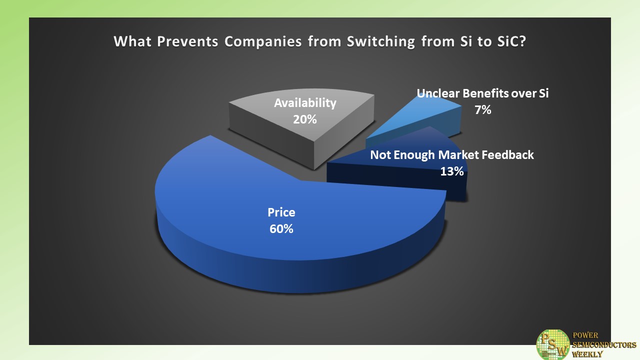
Despite the fast growth and penetration into the power electronics market, many companies still feel uncomfortable when they hear about silicon carbide and the benefits it has. During numerous negotiations and talks with the companies using power semiconductor devices, I shortlisted the most common barriers preventing them from switching from silicon to silicon carbide, or from increasing the number of SiC-based projects they already have.
To further scale this data, recently I had a poll on LinkedIn within the power electronics community. A similar poll I ran during the latest EPE’23 ECCE Europe Conference, which was held in Aalborg, Denmark. Both polls’ participants come from power semiconductors companies or from companies using power semiconductors.
Combined poll results look like this:
- Price – 60%
- Availability – 20%
- Unclear benefits over Si – 7%
- Not enough market feedback – 13%
It is clear that price is still the major concern and barrier. Even though the price has tremendously decreased during the past ten years, it remains one of the key factors why many companies prefer to use Si-based semiconductors.
The availability of SiC wafers or SiC-based devices accounts for another 20% of doubts coming from the end users. The lead time of SiC has been discussed many times, and the situation for many stays unclear. And it is the same for the remaining 20% of poll results coming from unclear benefits of SiC and lack of market feedback. Silicon power devices have been in use for decades, while SiC is just at the beginning of its road. That is why many engineers prefer to work with the technology they know, the technology they have been very familiar with since their school.
From the first look the answers and results of the poll seem to be right and they correspond to the current market situation. However, working with Si and SiC, I know that each and every one of the answers listed are just the barriers and not the final verdict.
Semiconductor companies should pay more attention to those 20% of the answers referring to lack of market data. With the right approach SiC will bring the power semiconductors industry to a new level.
-
Power semiconductors based on silicon carbide (SiC) offer several advantages, like high efficiency, power density, voltage resistance, and reliability. This creates opportunities for new applications and improved charging station technology innovations. Infineon Technologies announced a collaboration with Infypower, a Chinese market leader in new energy vehicle charging. Infineon will provide INFY with the industry-leading 1200 V CoolSiC™ MOSFET power semiconductor devices to improve the efficiency of electric vehicle charging stations.
“The collaboration between Infineon and Infypower in the field of charging solutions for electric vehicles (EV) provides an excellent system-level technology solution for the local EV charging station industry,” said Dr. Peter Wawer, Division President of Infineon’s Green Industrial Power Division. “It will significantly improve charging efficiency, accelerate charging speed, and create a better user experience for owners of electric cars.”
“With Infineon’s more than 20 years of continuous advancement in SiC product offering and the strength of integrated technology, Infypower can consolidate and maintain its technological outstanding position in the industry by adopting state-of-the-art product processes and design solutions“, said Qiu Tianquan, President of Infypower China. “We can also set a new standard for charging efficiency of DC chargers for new energy vehicles. As a result, customers can enjoy more convenience and unique value, promoting the healthy development of the EV charging industry.”
SiC’s high power density enables the development of high-performance, lightweight, and compact chargers, especially for supercharging stations and ultra-compact wall-mounted DC charging stations. Compared to traditional silicon-based solutions, SiC technology in EV charging stations can increase efficiency by 1 percent, reducing energy losses and operating costs. In a 100 kW charging station, this translates to 1 kWh of electricity savings, saving 270 Euros annually and reducing carbon emissions by 3.5 tons. This drives the increasing adoption of SiC power devices in EV charging modules.
As one of the first SiC power semiconductor manufacturers to use trench gate technology for transistors, Infineon has introduced an advanced design that provides high reliability for chargers. The devices offer a high threshold voltage and simplified gate driving . The CoolSiC MOSFET technology has been subjected to marathon stress tests and gate voltage jump stress tests before commercial release and regularly afterwards in form of monitoring to ensure highest gate reliability.
By integrating Infineon’s 1200 V CoolSiC MOSFETs, Infypower’s 30 kW DC charging module offers a wide constant power range, high power density, minimal electromagnetic radiation and interference, high protection performance and high reliability. In this way, it is well suited for the fast charging demand of most EVs while possessing a higher efficiency of 1 percent compared with other solutions on the market. Consequently, significant energy savings and carbon dioxide emission reduction are achieved, which are leading at a global level.
Original – Infineon Technologies
-

Aehr Test Systems announced it has received an initial customer order for a FOX-NP™ wafer level test and burn-in system, multiple WaferPak™ Contactors, and a FOX WaferPak Aligner to be used for engineering, qualification, and small lot production wafer level test and burn-in of their silicon carbide devices. The customer is a US-based multibillion-dollar semiconductor supplier serving several markets including automotive, computing, consumer, energy, industrial, and medical. The FOX-NP system, including the FOX WaferPak Aligner and initial WaferPaks are scheduled per the customer’s requested accelerated schedule to ship by the end of the calendar year 2023.
The FOX-NP system is configured with the new Bipolar Voltage Channel Module (BVCM) and Very High Voltage Channel Module (VHVCM) options that enable new advanced test and burn-in capabilities for silicon carbide power semiconductors using Aehr’s proprietary WaferPak full wafer Contactors. This new order highlights Aehr’s continued progression within the growing silicon carbide global power market.
Gayn Erickson, President and CEO of Aehr Test Systems, commented, “We are very excited that after conducting a detailed financial evaluation and multiple onsite visits to Aehr’s application lab, this new customer selected our FOX-P solution for engineering, qualification, and production of their silicon carbide power devices.
This evaluation included cost of ownership and system throughput, as well as device test, burn-in, and stabilization coverage. As their production capacity increases, they told us that they will quickly move to our FOX-XP multi-wafer test and burn-in systems for high-volume production. In addition to the automotive electric vehicle device opportunity, this customer in particular sees the enormous opportunity for silicon carbide power devices in industrial, solar, and other power applications.
“William Blair forecasts that in addition to the 4.5 million six-inch equivalent wafers that will be needed to meet the demand for electric vehicle related silicon carbide devices in 2030, another 2.8 million wafers are needed to address industrial, solar, electric trains, energy conversion and other applications in 2030. The interesting part of this is that most of these applications will be served with discrete MOSFETS in single die packages.
The cost of ownership of our solution proved to be more cost-effective and efficient for these devices than package part burn-in after the die are packaged in packages such as TO-247 or other discrete packages. This is a strong testimony of the advantage of wafer level burn-in as a better alternative to package part burn-in. This expands our silicon carbide test and burn-in market even more and this new customer helps expand Aehr’s presence in this market as our total addressable market (TAM) continues to grow.
“Aehr’s FOX-P systems and proprietary WaferPak full wafer Contactors enable our customers to do economical production volume test and reliability burn-in with processes such as High Temperature Gate Bias (HTGB) and High Temperature Reverse Bias (HTRB) very cost-effectively and ensure extremely high device quality. Our systems are typically used for long burn-in times lasting up to 24 hours or more.
We can do this for under $5.00 per hour per wafer capital depreciation cost while testing and burning-in up to several thousand devices at a time per wafer. This is also in a test system footprint that is up to 94% less than a typical test system on a standard semiconductor wafer prober, which in a precious clean room wafer facility is extremely important and saves a great deal of cost.
“The FOX family of compatible systems including the FOX-NP and FOX-XP multi-wafer test and burn-in systems and Aehr’s proprietary WaferPak full wafer contactors provide a uniquely cost-effective solution for burning in multiple wafers of devices at a single time to remove early life failures of silicon carbide devices, which is critical to meeting the initial quality and long-term reliability of the automotive, industrial, and electrification infrastructure industry needs.”
The FOX-XP and FOX-NP systems, available with multiple WaferPak Contactors (full wafer test) or multiple DiePakTM Carriers (singulated die/module test) configurations, are capable of functional test and burn-in/cycling of devices such as silicon carbide and gallium nitride power semiconductors, silicon photonics as well as other optical devices, 2D and 3D sensors, flash memories, magnetic sensors, microcontrollers, and other leading-edge ICs in either wafer form factor, before they are assembled into single or multi-die stacked packages, or in singulated die or module form factor.
Original – Aehr Test Systems
-
AIXTRON SE supports GlobiTech Inc., one of the world’s largest silicon-epitaxy foundries, to expand their business into silicon carbide (SiC) epitaxy. AIXTRON’s new G10-SiC has enabled this global leader to quickly ramp its SiC epitaxy production into high volume to address the world’s increasing demand for power epi-wafers. GlobiTech’s selection of the G10-SiC means a future-proof investment based on dual wafer size configuration of 9×150 & 6×200 mm and the highest throughput per fab space available in the SiC industry today.
The G10-SiC was officially introduced in September 2022. And it has quickly become the tool of record for both 150mm and 200mm SiC device makers as well as foundries like GlobiTech, the wholly owned subsidiary of GlobalWafers Co., Ltd., which manufactures silicon carbide and silicon epitaxial wafers focused on power and electric vehicle (EV) market segments.
“When one of the largest manufacturers and foundries like GlobiTech diversifies its business, it is a clear signal of a long-lasting trend in the semiconductor industry: conventional silicon is being replaced by silicon carbide in an ever-increasing number of applications. And it makes us proud when a leading company such as GlobiTech chooses AIXTRON and our new G10-SiC as an enabler of its transition intothis emerging SiC market. It confirms our overall strategy and the prospects for further growth”, says Dr. Felix Grawert, CEO and President of AIXTRON SE.
GlobiTech, located in Sherman, TX, is already in high-volume production using both G5WW C and G10-SiC AIXTRON systems, with continued installation capacity over the next years.Modeled after the silicon business, GlobiTech supplies both SiC substrates and SiC epitaxy to the market.
“In AIXTRON, we have found a strong partner supporting us in our vision and plans to expand our business into the SiC epitaxy market – an important step as SiC technology is one of the fastest-growing semiconductor sectors. AIXTRON tools allow us to get the most wafers out of our current fab. And AIXTRON’s team understands what it takes to compete against silicon to grow this market while offering great customer support and service”, says Mark England, President of GlobalWafers.
The G10-SiC is the first SiC epitaxy tool on the market that truly enables high-volume production of SiC epi-wafers. Since the G10-SiC offers both 9×150 mm and 6×200 mm batch configurations, it is an instrumental tool for a market rapidly transitioning from 6-inch (150mm) to 8-inch (200 mm) wafer diameters. The new platform is built around AIXTRON’s proven automated wafer cassette-to-cassette loading solution with high-temperature wafer transfer.
Combined with high growth rate process capabilities, the G10-SiC provides best-in-class wafer throughput, an excellent epi wafer performance in terms of quality and uniformity, and the best throughput per square meter of fab space. All this leads to the lowest cost of ownership in the market. It is estimated that in 2023, the new G10-SiC will become AIXTRON’s top-selling product.
The wide-bandgap material SiC is set to become mainstream technology for efficient power electronics. Driven by the growing adoption of SiC-based power semiconductors within e-mobility solutions and the overall acceleration of the charging infrastructure, the global demand for SiC wafers is growing rapidly.And with its superior characteristics, SiC semiconductors offer higher energy efficiency than conventional power electronics based on silicon. Therefore, SiC significantly contributes to reducing the global CO2 footprint.
Original – AIXTRON
-
Semilab announced an agreement to form a long-term strategic partnership with Fraunhofer IISB. Within the framework of this cooperation, a demo lab will be opened with a strong focus on developing state-of-the-art metrology and inspection solutions for wide bandgap semiconductor materials.
Over the years, developments in compound semiconductor materials such as silicon carbide (SiC) have been receiving increased attention. SiC devices show great promise in the future of wide bandgap semiconductors due to their superior material properties. The silicon carbide market’s growth shows no sign of slowing down due to the expansion in the industrial and automotive sectors. Semilab believes in driving decarbonization by supporting the development of key SiC products and components.
Based in Budapest, Hungary, Semilab is a strategic metrology supplier and innovation partner of the leading wafer manufacturers, IC device makers in the More-than-Moore market segment. Semilab provides state-of-the-art metrology solutions for semiconductor device manufacturers, both in-line and R&D segments. The company is among the world leaders in non-contact CV metrology for SiC and its market share is growing for EPI thickness and resistivity monitoring.
The Fraunhofer IISB in Erlangen, Germany, specializes in wide-bandgap semiconductors and efficient power electronics. Here, device know-how merges with complex system development, especially for e-mobility and sustainable energy supply.
The institute bundles its activities in the two business units Power Electronic Systems and Semiconductors. In doing so, it comprehensively covers the entire value chain from basic materials, through semiconductor device, process and module technologies, to complete electronics and energy systems. As a unique center of excellence in Europe for the semiconductor material silicon carbide (SiC), the IISB is a pioneer in the development of highly efficient power electronics, even for extreme requirements. This spans from material, over process and to device development supported by providing innovative metrology solutions.
Considering the crucial role both players have in shaping of the European semiconductor scene, the strategic partnership between Semilab and Fraunhofer IISB will allow the utilization of their respective resources and global networks in order to develop new, innovative silicon carbide processes and metrologies.
Original – Semilab
-
Navitas Semiconductor announced participation at the International Conference on Silicon Carbide and Related Materials (ICSCRM) 2023, to be held in Sorrento, Italy.
The ICSCRM conference fosters collaboration and knowledge sharing among the brightest minds in the field. The conference has a rich history dating back to its inaugural meeting in 1987, evolving into a premier global forum for in-depth technical discussions on all aspects of SiC and related materials.
GeneSiC™ power devices, optimized for high-power, high-voltage, and high-reliability SiC applications, address critical markets including electric vehicles, solar energy, energy storage, industrial applications, data centers, and consumer electronics. With an unmatched voltage range spanning from 650 V to 6.5 kV, GeneSiC MOSFETs and Schottky MPS™ diodes have been at the forefront of SiC technology advancement, offering performance and efficiency that pave the way for a more electrified and sustainable future.
Navitas Semiconductor will present two paper sessions at ICSCRM 2023:
- “New Generation SiC MPS Diodes with Low Schottky Barrier Height”
- “650 V SiC Power MOSFETs with Statistically Tight VTH Control and RDS(ON) of 1.92 mΩ-cm²”
Additionally, Navitas’ SVP of SiC Technology & Operations, Dr. Sid Sundaresan, will be chairing the session on Thursday, September 21st. The session, titled “Devices 4: Short circuit, avalanche and reliability,” will focus on crucial topics in the field of SiC technology.
“Navitas’ presence at ICSCRM 2023 is a testament to the company’s unparalleled expertise in SiC technology and its commitment to driving innovation in the industry,” said Dr. Ranbir Singh, Navitas EVP for the GeneSiC business line. “As a pioneer in the field, we continue to extend the boundaries of SiC technology, revolutionizing power semiconductors with cutting-edge GeneSiC™ technology.”
Original – Navitas Semiconductor
-
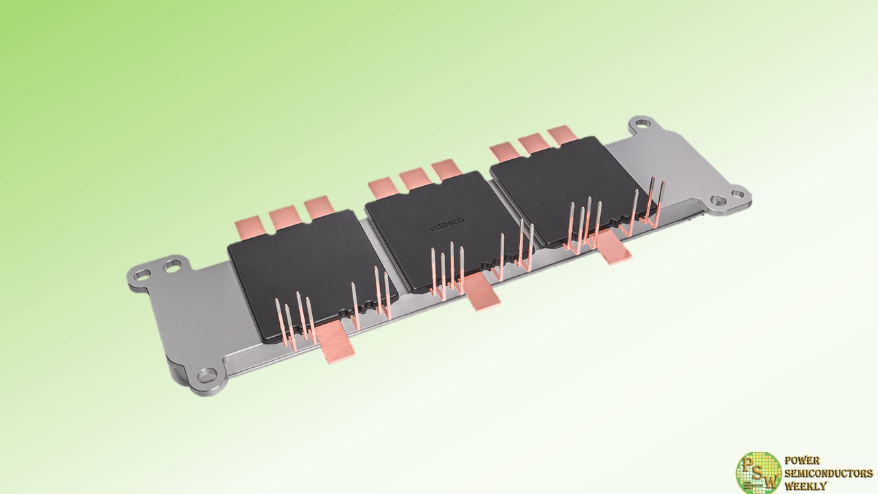
Vitesco Technologies is developing a power module which will be manufactured using transfer molding process. During this process the power electronics are sealed under a dielectric material that protects the components extremely well. The result is a very robust, cost effective and reliable electronic. The power module consists of three overmolded half-bridges and forms the core of an inverter system, which controls both the drive energy and the energy recovery (recuperation) in high-voltage electric vehicles.
Manufactured at the Nuremberg electronics plant, the power modules will be delivered to a large global car maker from mid-2025 onwards.
Vitesco Technologies has been adapting and utilizing transfer molding technology since 2020, first applying it to compact Transmission Control Units designed for full integration inside a gear box.
The overmold power modules now combine highly efficient state-of-the art silicon carbide (SiC) chip technology with overmolding to facilitate a particularly robust product with increased power density, lower cost and reduced weight.
These power modules are a good example of strategic approach of using the scalability and modularity of our power electronics to develop and manufacture submodules in addition to the complete electronics. Combined with extensive overmolding expertise, Vitesco can deliver an extremely robust product to our customers. This is yet another example of how the company successfully transfers proven technology to an electrification product.
- Thomas Stierle, member of the board and head of Vitesco Technologies’ Electrification Solutions division
Vitesco Technologies has extensive expertise in power electronics and is already on the market with its fourth generation. The newly developed overmold power module expands the company’s strategic portfolio.
A very deep system competence is necessary to ensure that a sub-module of this kind, which forms the core of the inverter, can be successfully integrated into the full system. Our degree of electronics modularity and scalability enables us to offer more flexibility in terms of customer-specific interfaces.
- Michael Horbel, head of product and platform management high voltage inverter at Vitesco Technologies
Vitesco Technologies will continue to use this strength to bring further electronic sub-modules to the market.
The lead plant for these modules is Vitesco Technologies’ Nuremberg site. With its existing competencies and experience, the plant offers a high degree of automation as well as the focus on electronics and e-mobility required for the power modules. This is a further step forward into the “Plant of the Future” concept, defined for the Nuremberg plant to maintain its international competitiveness.
Original – Vitesco Technologies
-
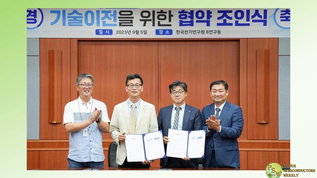
Korea Electrotechnology Research Institute (KERI) succeeded in transferring the ‘Ion Implantation and its Evaluation Technology for the SiC (silicon carbide) Power Semiconductor’ to a Hungarian company.
Power semiconductors are key components in electricity and electronics, acting as the muscles of the human body by regulating the direction of current and controlling power conversion. There are many different materials for power semiconductors. Among them, SiC is receiving the most attention due to its excellent material properties, including high durability and excellent power efficiency. When SiC power semiconductors are incorporated into electric vehicles, they cut down the power consumption of the battery and reduce the body weight and volume of the vehicle, resulting in energy efficiency improvements of up to 10%
While SiC power semiconductors have many advantages, the manufacturing process is also very challenging. Previously, a method was applied to create a device by forming an epi layer (single-crystal semiconductor thin-film) on a highly conductive wafer and flowing current through that area. However, during this process, the surface of the epi layer becomes rough and the speed of electron transfer decreases. The price of the epi wafer itself is also high, which is a major obstacle to mass production.
To solve this problem, KERI used a method of implanting ions into a semi-insulated SiC wafer without an epi layer. Ion implantation, which makes a wafer conductive, is the work that breathes life into a semiconductor.
SiC materials are hard and require very high energy ion implantation followed by high temperature heat treatment to activate the ions, making it a difficult technology to implement. However, KERI has succeeded in securing the relevant technologies based on its 10 years of experience in operating ion implantation equipment dedicated to SiC.
“Ion implantation technology can significantly reduce process costs by increasing current flow in semiconductor devices and replacing expensive epi wafers,” said Dr. Kim, Hyoung Woo, Director, Advanced Semiconductor Research Center, KERI. He continued, “This is a technology that increases the price competitiveness of high-performance SiC power semiconductors and contributes greatly to mass production.”
This technology was recently transferred to ‘SEMILAB ZRT (CEO: Tibor Pavelka)’, a semiconductor metrology equipment company located in Budapest, Hungary. With a 30-year history, SEMILAB has manufacturing plants in Hungary and the United States. SEMILAB owns patents for medium-sized precision measurement equipment and material characterization equipment, and has the world’s leading technology in semiconductor electrical parameter evaluation system.
They predict that through this technology transfer, they will be able to standardize high-quality SiC. SEMILAB plans to use KERI technology to develop specialized equipment to evaluate the ion implantation process of SiC power semiconductor.
Park Su-yong, the president of SEMILAB Korea, said, “Through the development of specialized equipment, we will be able to progress in-line monitoring of implant processes on SiC wafers for immediate, accurate, and low-cost production control of implant systems and in-line monitoring for pre-anneal implant.” He added, “This will be a great foundation for stably securing a high-quality ion implantation mass production process with excellent uniformity and reproducibility.”
KERI is a government-funded research institute under the NST (National Research Council of Science & Technology) of the Ministry of Science and ICT. It has a total of more than 120 intellectual property rights in the field of power semiconductor research. As of the last 10 years, power semiconductor division of KERI has achieved more than KRW 3 billion in technology transfers, the highest level in South Korea.
Original – KERI
