-

On the road towards becoming a fully electric car maker by 2030, an important focus area for Volvo technology investments and R&D spending is e-motors, inverters and overall electric drivetrain optimisation.
Only by gaining control over electrification technology stack – a process called “vertical integration” – can can a company create pure electric Volvo cars that deliver on everything the customers want: longer range, faster charging and a great Volvo driving experience.
The latest investment by the Volvo Cars Tech Fund, the corporate venture capital arm, reflects those ambitions. Leadrive, a Shanghai-based company founded in 2017, is an exciting new player in power electronics and control units for fully electric cars.
Leadrive is specialising in designing and building power modules that use silicon carbide (SiC) technology. Silicon carbide is a semiconductor base material that promises to unlock highly efficient and flexible electric propulsion systems.
“Leadrive’s technology demonstrates a lot of potential for the development of more efficient electric drivetrains,” said Alexander Petrofski, CEO of the Volvo Cars Tech Fund. “That potential closely aligns with our own focus on electrification, so we’re excited to invest in the company and help it to continue growing its business.”
“Volvo Cars and Leadrive have been working very closely on the development of new generation SiC technologies, which has built a firm stairway towards the strategic collaboration,” said Jie Shen, founder and CEO of Leadrive. “This is a great milestone in Leadrive’s global strategy and demonstrates the huge potential of our cooperation in advanced electrification technology.”
Original – Volvo Car Corporation
-
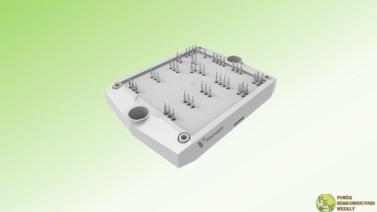
The new Vincotech 1200 V flowCSPFC S3 SiC module featuring current-synthesizing PFC (CS-PFC) topology based on the constant power control, strikes the best balance between performance and system cost to benefit your business.
The first module of this new product family is well suited for a DC fast charger PFC converter stage up to 35kW power, a “sweet spot” for building scalable DC charger units on a modular approach.
Main benefits
- Current-synthesizing PFC slashes module costs by > 25% with conversion efficiencyranging as high as >99%
- System costs come down with fewer and smaller inductors on the PCB
- No large electrolytic DC-link capacitors for even more system-level savings
- Pinout is ready for bidirectional applications and optimized for easy PCB routing
- High power density for compact designs and fast charging
Applications
- EV fast charger
- UPS
- ESS
Original – Vincotech
-
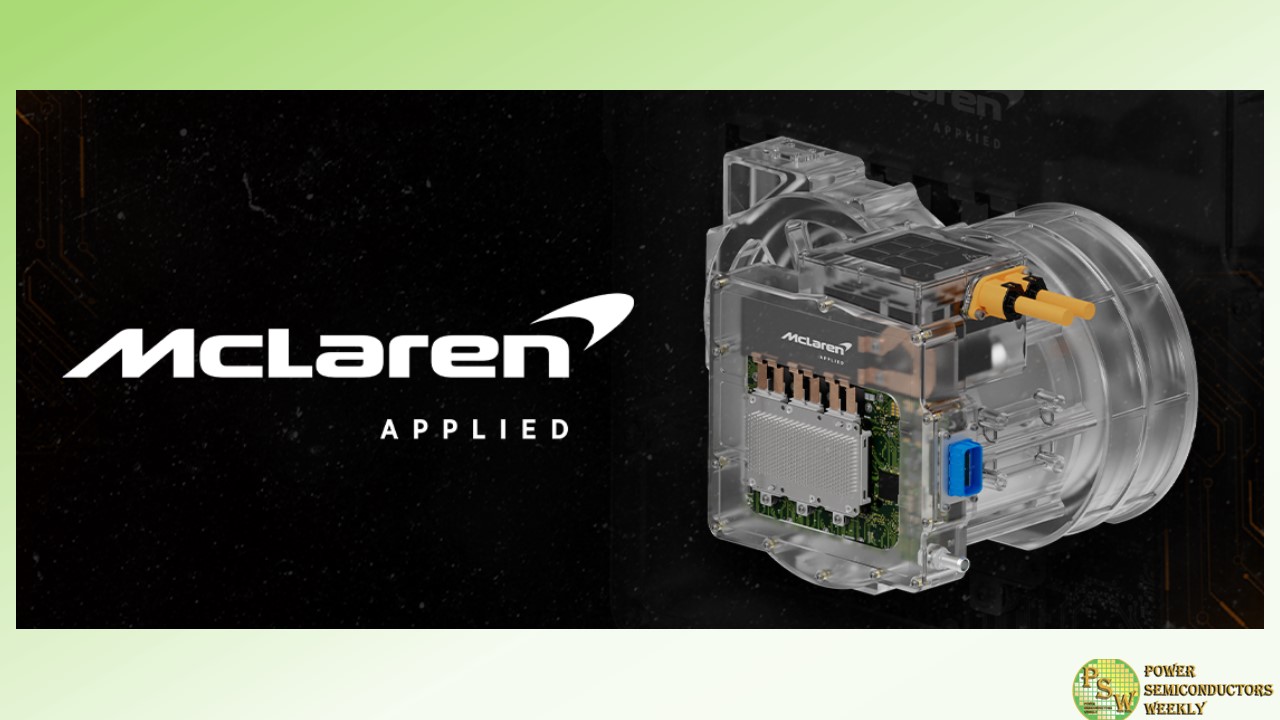
McLaren Applied has launched IPG5-x, a highly flexible 800V Silicon Carbide (SiC) inverter that can be integrated into Electric Drive Units (EDUs). Targeting growing OEM demand for high-performing, integrated EDUs that save space and cost, the British engineering and technology pioneer has developed IPG5-x to work with a variety of motors and transmissions – especially in performance applications.
IPG5-x is an adaptation of McLaren Applied’s current award-winning 800V SiC inverter, IPG5. IPG5-x will coexist alongside the standalone IPG5, with application depending on customer need. The ‘x’ suffix was chosen because IPG5-x is a product designed for collaboration with Tier 1 and OEM partners looking to bring EDU products to market quickly and cost effectively. McLaren Applied is in discussions with several OEMs and Tier 1 suppliers, and is working with transmission provider TREMEC to jointly develop an integrated EDU for their first customer vehicle application.
“In our discussions with customers and partners, it’s become clear that OEMs are increasingly looking for the option to source integrated EDUs that save space, cost and speed up development time,” commented Paolo Bargiacchi, Head of Product, Automotive at McLaren Applied. “We’ve developed the IPG5-x to be highly flexible, so it’s ready to be integrated within any combination of motor and transmission. It carries over all of our standalone IPG5’s qualities – peak efficiencies over 99%, continuously variable switching and fine motor control – building on the maturity of that product.”
Derived from decades of innovation in top tier automotive and motorsports, McLaren Applied’s IPG5-x offers best-in-class fine motor control and high efficiency through continuously variable switching frequencies; maximising the advantages of SiC semiconductors.
The IPG5-x forms a step forward in what the automotive team at McLaren Applied describes as the ‘waves of electrification’. The first wave involved early pioneers of technology, the second wave is denoted by the breakthrough of EVs to the mainstream. The third wave is efficiency and will see inverter technology rapidly adopt SiC semiconductors, especially in 800V architectures, enabling vehicles to achieve longer range where efficient power electronics are key.
Bargiacchi added: “The immediate focus must be on achieving greater drivetrain efficiency and cost reduction, which you can do through a product like IPG5-x. The competitive landscape is ramping up significantly now that all manufacturers have established their product entry points.
“Models based on dedicated 800V SiC architectures are leading the way, driving a virtuous cycle: an efficient drivetrain inherently has a smaller battery, which makes the vehicle cheaper, lighter and easier to control, and offers a smaller embedded and operating carbon footprint. It also increases range and speeds up charge times, building trust in the technology.”
As competition increases, we will enter the fourth wave, where OEMs will need to differentiate the customer experience their products deliver. In anticipation of this change, McLaren Applied has developed advanced motor control software in both IPG5 and IPG5-x that enables a variety of features ranging from improved refinement through to a more engaging drive.
Original – McLaren Applied
-
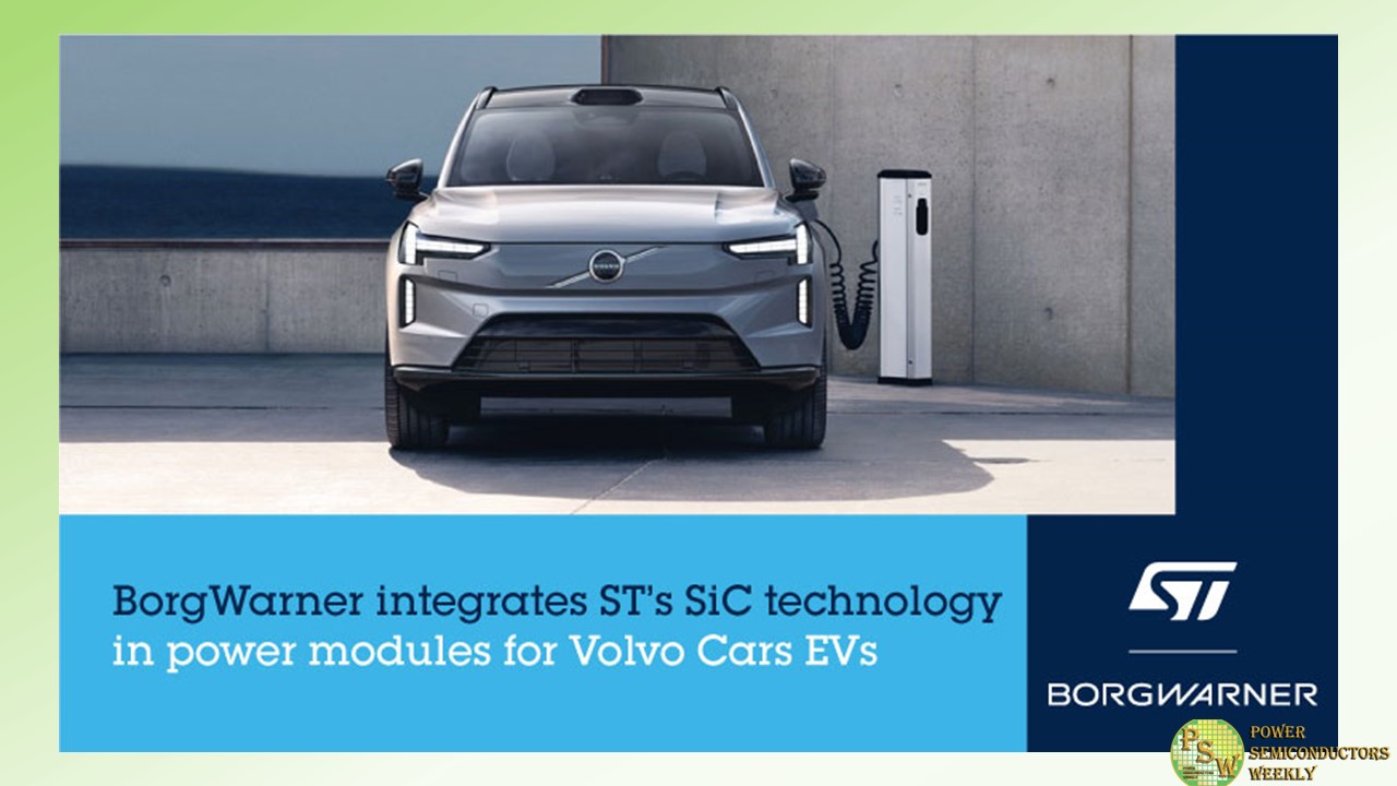
STMicroelectronics will supply BorgWarner Inc. with the latest third generation 750V silicon carbide (SiC) power MOSFETs dice for their proprietary Viper-based power module. This power module is used in BorgWarner’s traction inverter platforms for several current and future Volvo Cars electric vehicles.
“This collaboration will give Volvo Cars the opportunity to further increase the attractiveness of our electrical vehicles with longer range and faster charging. It will also support us on our journey towards being fully electric by 2030 and strengthen our increased vertical integration and our control of critical components,” says Javier Varela, Chief Operating Officer & Deputy CEO, Volvo Cars.
“BorgWarner is pleased to partner with ST to supply our longstanding customer Volvo Cars with inverters for their next generation of BEV platforms,” says Stefan Demmerle, Vice President of BorgWarner Inc. and President and General Manager, PowerDrive Systems.
To fully leverage the performance of ST’s SiC MOSFET dice, BorgWarner collaborated closely with ST’s technical team to match their die with BorgWarner’s Viper power switch, thereby maximizing inverter performance and delivering a compact and cost-effective architecture. The collaboration between the companies provides the high-volume capability that is required by the quickly growing EV market.
“Our collaboration with BorgWarner, a leading global automotive supplier in electrification, will enable Volvo Cars to offer their customers superior vehicle performance and range,” says Marco Monti, President, Automotive and Discrete Group, STMicroelectronics. “We are committed to expanding SiC capacity and to reinforcing our SiC supply, including through vertical integration, as we ramp up volumes to support our global automotive and industrial customers in their shift to electrification and higher efficiency.”
ST’s high-volume STPOWER SiC products are manufactured in its fabs in Italy, and Singapore, with advanced packaging and testing at its back-end facilities in Morocco and China. In October 2022, ST announced it would expand its wide bandgap manufacturing capacity with a new integrated SiC substrate manufacturing facility in Catania, home to the company’s power semiconductor expertise and the site of integrated research, development, and manufacturing of SiC.
Original – STMicroelectronics
-
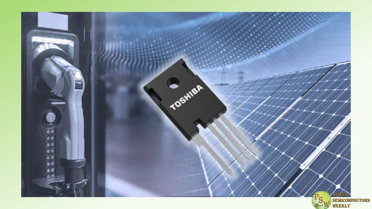
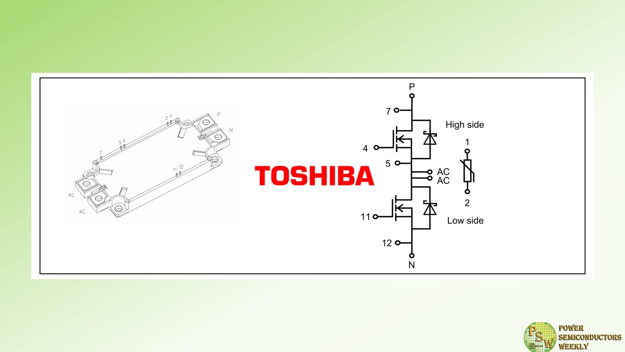
Toshiba Electronic Devices & Storage Corporation has launched silicon carbide (SiC) MOSFETs, the “TWxxxZxxxC series,” that use a four-pin TO-247-4L(X) package that reduces switching loss with the company’s latest 3rd generation SiC MOSFETs chip for industrial equipment. Volume shipments of ten products, five with 650V ratings and five with 1200V, start today.
The new products are the first in Toshiba’s SiC MOSFET line-up to use the four-pin TO-247-4L(X) package, which allows Kelvin connection of the signal source terminal for the gate drive. The package can reduce the effect of source wire inductance inside the package, improving high-speed switching performance. For the new TW045Z120C, the turn-on loss is approximately 40% lower and the turn-off loss reduced by approximately 34%, compared with Toshiba’s current product TW045N120C in a three-pin TO-247 package. This helps to reduce equipment power loss.
Applications
- Switching power supplies (servers, data centers, communications equipment, etc.)
- EV charging stations
- Photovoltaic inverters
- Uninterruptible power supplies (UPS)
Features
- Four-pins TO-247-4L(X) package:
Switching loss is reduced by Kelvin connection of the signal source terminal for the gate drive - 3rd generation SiC MOSFETs
- Low drain-source On-resistance x gate-drain charge
- Low diode forward voltage: VDSF=-1.35V (typ.) (VGS=-5V)
Original – Toshiba
-
Toshiba Electronic Devices & Storage Corporation developed “MG250YD2YMS3,” the industry’s first 2200V dual silicon carbide (SiC) MOSFET module for industrial equipment. The new module has a drain current (DC) rating of 250A and uses the company’s third generation SiC MOSFET chips. It is suitable for applications that use DC1500V, such as photovoltaic power systems and energy storage systems. Volume shipments start today.
Industrial applications like those mentioned above generally use DC1000V or lower power, and their power devices are mostly 1200V or 1700V products. However, anticipating widespread use of DC1500V in coming years, Toshiba has released the industry’s first 2200V product.
MG250YD2YMS3 offers low conduction loss with a low drain-source on-voltage (sense) of 0.7V (typ.). It also offers lower turn-on and turn-off switching loss of 14mJ (typ.) and 11mJ (typ.) respectively, an approximately 90% reduction against a typical silicon (Si) IGBT. These characteristics contribute to higher equipment efficiency. Realizing low switching loss also allows the conventional three-level circuit to be replaced with a two-level circuit with a lower module count, contributing to equipment miniaturization.
Toshiba will continue to meet the market needs for high efficiency and the downsizing of industrial equipment.
Applications
Industrial Equipment
- Renewable energy power generation systems (photovoltaic power systems, etc.)
- Energy storage systems
- Motor control equipment for industrial equipment
- High frequency DC-DC converter, etc.
Features
- Low drain-source on-voltage (sense):
VDS(on)sense=0.7V (typ.) (ID=250A, VGS=+20V, Tch=25°C) - Low turn-on switching loss:
Eon=14mJ (typ.) (VDD=1100V, ID=250A, Tch=150°C) - Low turn-off switching loss:
Eoff=11mJ (typ.) (VDD=1100V, ID=250A, Tch=150°C) - Low stray inductance:
LsPN=12nH (typ.)
Original – Toshiba
-
Navitas Semiconductor will reveal a new, high-performance wide bandgap power platform as part of its display at one of Asia’s most prestigious electronics exhibitions – sponsored by Navitas – SEMICON Taiwan 2023, from September 6th-8th.
Visitors will discover the latest gallium nitride (GaN) GaNFast™ power ICs integrate gallium nitride (GaN) power and drive, with control, sensing, and protection to enable faster charging, higher power density, and greater energy savings. Complementary GeneSiC™ power devices are optimized high-power, high-voltage, and high-reliability silicon carbide (SiC) solutions.
Additionally, Navitas will showcase cutting-edge, power-system platforms to dramatically accelerate customer developments, minimize time-to-market, and set new industry benchmarks in energy efficiency, power density and system cost. These system platforms include complete design collateral with fully-tested hardware, embedded software, schematics, bill-of-materials, layout, simulation and hardware test results. Examples include:
- Navitas’ CRPS185 data center power platform, that delivers a full 3,200 W of power in only 1U (40 mm) x 73.5mm x 185 mm (544 cc), achieving 5.9 W/cc, or almost 100 W/in3 power density. This is a 40% size reduction vs, the equivalent legacy silicon approach and reaches over 96.5% efficiency at 30% load, and over 96% stretching from 20% to 60% load, creating a ‘Titanium Plus’ benchmark.
- Navitas’ 6.6 kW 3-in-1 bi-directional EV on-board charger (OBC) with 3 kW DC-DC. This 96%+ efficient unit has over 50% higher power density, and with efficiency over 95%, delivers up to 16% energy savings as compared to competing solutions.
As part of SEMICON’s Power and Opto Semiconductor Forum, Navitas’ Charles Bailley, Senior Director of Business Development, will present “GaN Power ICs Increase Power Density in EV Power Systems”. The presentation is at 2pm, on September 6th, in room 402, 4F, TaiNEX 1.
“Breakthrough high efficiency, high reliability, and high power density – all from the new GaN power IC platform,” said Kevin 汪時民 Wang, Manager of Navitas Taiwan. “The new platform announcement matches SEMICON’s theme of ‘Innovating the World through Semiconductors’ and our own mission to ‘Electrify Our World™’.”
Original – Navitas Semiconductor
-

The University of Arkansas celebrated an important milestone with the groundbreaking on a building that Chancellor Charles Robinson suggested might someday rival the U of A’s most iconic structure, Old Main, in significance to the university and the state of Arkansas.
Robinson and other university leaders, including University of Arkansas System President Don Bobbitt and members of the U of A System Board of Trustees, as well as researchers and industry leaders, gathered at the Arkansas Research and Technology Park in South Fayetteville to celebrate construction of the national Multi-User Silicon Carbide Research and Fabrication Facility, or MUSiC.
The new semiconductor research and fabrication facility will produce microelectronic chips made with silicon carbide, a powerful semiconductor that outperforms basic silicon in several critical ways. The facility will enable the federal government – via national laboratories – businesses of all sizes, and other universities to prototype with silicon carbide, a capability that does not presently exist elsewhere in the U.S.
Work at the facility will bridge the gap between traditional university research and the needs of private industry and will accelerate technological advancement by providing a single location where chips can go from developmental research to prototyping, testing and fabrication.
“This fills a gap for our nation, allowing companies, national laboratories and universities around the nation to develop the low-volume prototypes that go from their labs to fab, ultimately scaling up to the high-volume manufacturing…” said Alan Mantooth, Distinguished Professor of electrical engineering and principal investigator for the MUSiC facility. “We fill that gap. And there’s no other place like it in the world. This is the only place that will be able to do that with silicon carbide.”
The 18,660 square-foot facility, located next to the National Center for Reliable Electrical Power Transmission at the research and technology park, will address obstacles to U.S. competitiveness in the development of silicon-carbide electronics used in a wide range of electronic devices, circuits and other consumer applications. The building will feature approximately 8,000 square feet of clean rooms for fabrication and testing.
Education and training within the facility will also accelerate workforce development, helping supply the next generation of engineers and technicians in semiconductor manufacturing, which Mantooth and other leaders have said is critical for bringing semiconductor manufacturing back to the U.S., after it was offshored in the late 1990s and early 2000s.
“This is truly a special day in the life of the University of Arkansas,” said Robinson. “This building, it really doesn’t need to be hyped. It is a very important building, and you just know it, important for our university, important for our state, important for our nation.”
Robinson invoked another groundbreaking, that of Old Main, the university’s oldest and best known structure, which the university celebrated Aug. 17, 1873, almost exactly 150 years ago.
“I took that 150th anniversary of the groundbreaking as a good sign that we are moving in a timely way,” Robinson said, “doing important work in establishing this building.”
Friday’s groundbreaking occurred a day after the university and the Arkansas Department of Commerce hosted the CHIPS AMERICA Summit, an event in which research, industry and governmental leaders discussed semiconductor-related opportunities resulting from the CHIPS (Creating Helpful Incentives to Produce Semiconductors) and Science Act passed by Congress in 2022. The event featured Adrienne Elrod, director of external and government affairs for the U.S. Department of Commerce’s CHIPS Program Office, U.S. Rep. Steve Womack and Arkansas Secretary of Commerce Hugh McDonald.
During the summit, Elrod stated that prior to the coronavirus pandemic, 90% of the world’s leading-edge chips were manufactured at one facility in Taiwan. The federal government prioritized the onshoring of this critical technology as a result of manufacturing and production shortages of essential computer chips during the pandemic.
“If America is going to compete and lead the world over the next century, we must invest in our technology and manufacturing,” Elrod said. “We want to make sure, at the very least, that we have two new large-scale clusters of leading- edge fabs created (in the United States).”
As Mantooth mentioned, the University of Arkansas can contribute to this effort on a fundamental level and is uniquely positioned to take advantage of opportunities offered by the CHIPS and Science Act, which is providing approximately $280 billion in funding to stimulate domestic research and manufacturing of semiconductors.
“The university is leaning forward and has now secured funding for projects important to microelectronics research and development,” Womack said during Thursday’s summit. “The university has positioned itself, as I say often, to be the preeminent university research location for microelectronics. … I am grateful for the bright minds at the University of Arkansas with a proven track record of success who will make this happen.”
Original – University of Arkansas
-

The rapid growth of technology over the past century brought us as many advantages as many disadvantages including the accelerating global warming with its dramatic consequences we face every day in various parts of the Earth. So far no one found a solution how to stop this process, but there are many solutions how to slow it down.
Today we try to respond to this challenge with carbon neutrality initiatives launched in many countries across the globe. And one of the major steps in this green society program is the electrification of passenger and commercial vehicles.
Right now, companies have various approaches to vehicle electrification including mild-hybrid electric vehicles MHEV, full hybrid electric vehicles HEV, plug-in hybrid electric vehicles PHEV, battery electric vehicles BEV, and fuel-cell electric vehicle FCEV. What some time ago seemed like a big step forward is a reality we live in now.
And to make this dream come true became possible with the help of power semiconductors. For a long time, semiconductors were used in the automotive industry, and the evolution of power semiconductor materials pushed the transition to the electrification of vehicles. Electric vehicles’ performance and cost depend on the technical level of the motor control system.
Previously, silicon (Si) IGBT modules served as the heart of electronic control systems with their relatively high switching speed and low conduction loss. But with the growth of silicon carbide (SiC) technology, EVs step into the new era of electrification.
Silicon-based semiconductors have been dominating the market for many decades. No wonder, several generations of power electronics engineers were passing their knowledge and experience working with silicon semiconductors. Through time they have short-listed their preferred solutions produced by several companies.
Based on the current requirements for the improvement of battery life and dynamic performance of electric passenger and commercial vehicles, higher efficiency, and fewer parts and materials are required to further improve the power density of inverters and electric drive assemblies. All this becomes possible with the transition from Si to SiC power devices. But when it comes to the all-new silicon carbide semiconductors and the rapidly growing EV industry, many face difficulties to make the right choice of the silicon carbide devices available in the market.
Recently I launched a poll to understand what is most important for EV companies when choosing a supplier of SiC power devices. Power electronics engineers from the semiconductor and automotive industries shared their experience and unanimously confirmed that the performance of the power devices plays a crucial role when choosing a supplier. The poll results are:
- Performance/characteristics – 66%
- Price – 16%
- Lead time – 9%
- Brand – 9%
Based on the results it is clear that for the EV market today characteristics of SiC power devices and price play the most important role. After all, consumers want high performance and reliability at affordable prices.
Nowadays SiC is still more expensive than Si. However, the prices have dropped a lot in the past decade, and the growing number of SiC fabs promises to drop the price in the future. Fingers crossed, in the nearest future, the dream of the consumers for the high-performance, reliable, and affordable EV will come true.
-
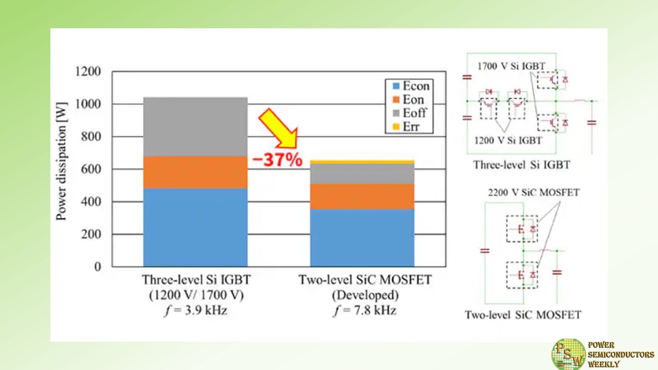
Toshiba Electronic Devices & Storage Corporation has developed 2200 V silicon carbide (SiC) metal oxide semiconductor field effect transistors (MOSFETs) for photovoltaic (PV) inverters. A two-level inverter with the new devices realized higher frequency operation and lower power loss than a conventional three-level silicon (Si) insulated gate bipolar transistor (IGBT) inverter. The new MOSFETs also contribute to simplification of inverter systems and reductions in their size and weight.
Three-level inverters enjoy the advantage of low switching losses because the voltage applied to switching devices in the inverters during off-state is half the line voltage. Against this, two-level inverters have fewer switching modules than three-level inverters, realizing a simpler, smaller, and lighter system. However, they require semiconductors with higher breakdown voltage, as the applied voltage is equal to the line voltage. Also, demand for semiconductors with both low loss and high breakdown voltage is growing as 1500 V DC line voltage systems are introduced in photovoltaic and other renewable energy markets.
Toshiba Electronic Devices & Storage Corporation has developed 2200 V Schottky barrier diode (SBD)-embedded SiC MOSFETs for two-level inverters in 1500 V DC voltage systems. The impurity concentration and thickness of the drift layer has been optimized to maintain the same relationship between the on-resistance and the breakdown voltage as our existing products, and also to achieve high resistance to cosmic rays, a requirement for PV systems. It has also been confirmed that embedding SBDs clamped parasitic PN junctions between the p-base regions and the n-drift layer secure high reliability in reverse conduction.
Switching energy loss for the developed all-SiC module is far lower than for the Si module (Si IGBTs + Si fast recovery diodes) with the same 2000 V rated voltage class. Estimates of inverter power dissipation found that the developed SiC module achieves higher frequency operation twice that of a conventional Si IGBT, as well as a 37% lower loss for the two-level SiC inverter against the three-level Si inverter. The higher frequency operation enables downsizing and weight reduction of other system components, such as heat sinks and filters.
Original – Toshiba
