-
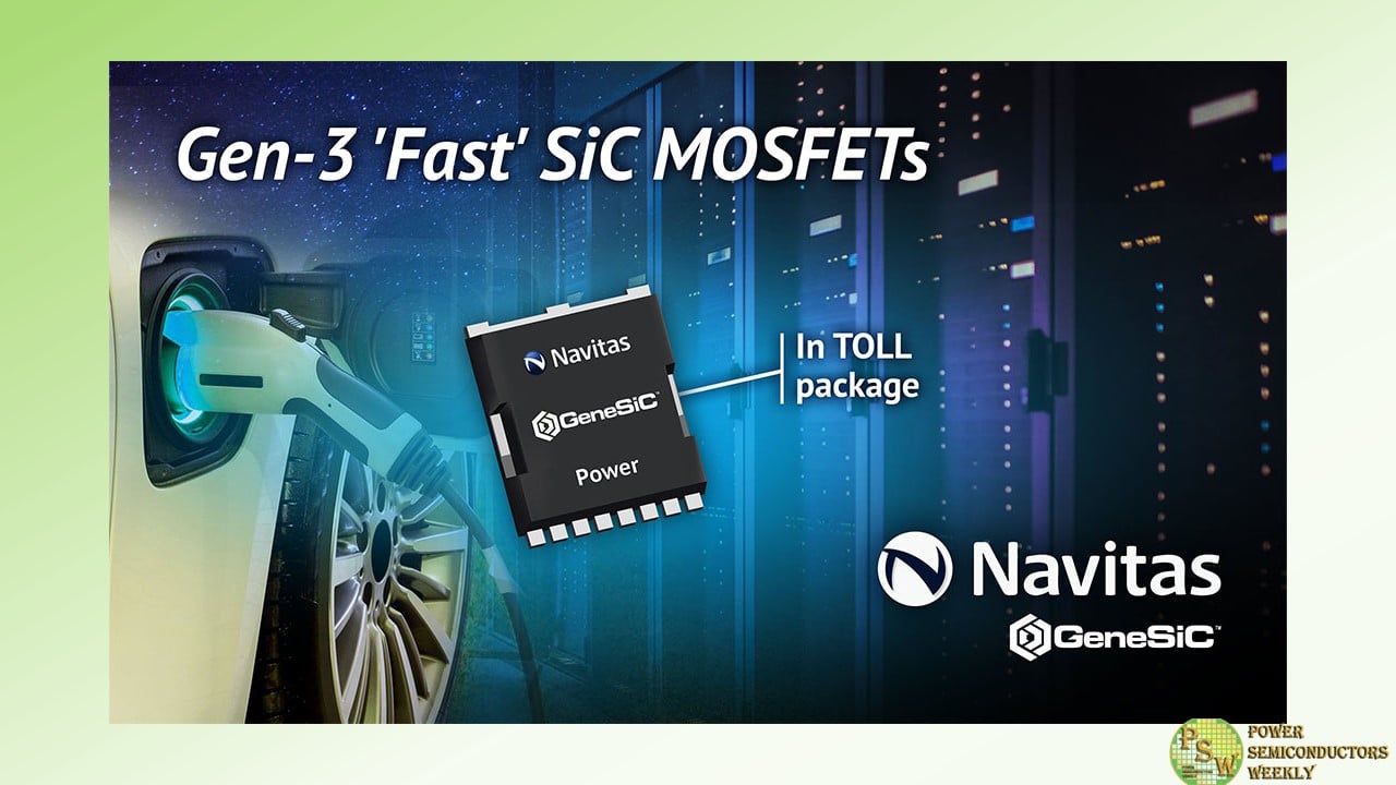
Navitas Semiconductor extended its new portfolio of Gen-3 ‘Fast’ (G3F) 650 V SiC MOSFETs into a thermally-enhanced, rugged, high-speed, surface-mount TOLL (Transistor Outline Leadless) package designed for demanding, high-power, high-reliability applications.
Combining high-power capability and best-in-class low on-resistance of 20 to 55 mΩ, these 650 V SiC MOSFETs have been optimized for the fastest switching speed, highest efficiency, and increased power density demanded by applications such as AI data center power supplies, EV charging and energy storage and solar solutions (ESS).
Navitas’ GeneSiC products use a proprietary ‘trench-assisted planar’ technology that provides world-leading efficiency performance over the temperature range, with G3F MOSFETs delivering high-speed, cool-running performance that ensures up to 25°C lower case temperatures and up to 3x longer life than alternative SiC products.
Navitas’ latest 4.5 kW AI power system reference design features the G3F45MT60L (650V 40 mΩ, TOLL) G3F SiC MOSFET in an interleaved CCM-TP PFC topology. Complemented by the NV6515 (650V, 35mΩ, TOLL) GaNSafe™ Power IC in the LLC stage, the 4.5 kW solution has a peak efficiency above 97% and, at 137 W/inch3, it is the world’s highest power density AI PSU. For 400 V-rated EV battery systems, G3F in TOLL is an ideal technology for on-board chargers (OBC), DC-DC converters, and traction drives ranging from 6.6 to 22 kW.
The surface-mount TOLL package offers a 9% reduction in junction-to-case thermal resistance (RTH,J-C), 30% smaller PCB footprint, 50% lower height, and 60% smaller size than the traditional D2PAK-7L, enabling highest-power-density solutions, as demonstrated in the 4.5 kW AI solution. Additionally, with a minimal package inductance of only 2 nH, excellent fast-switching performance and lowest dynamic losses are achieved.
The G3F family in TOLL package is released and available for purchase.
Original – Navitas Semiconductor
-

Toshiba Electronic Devices & Storage Corporation and Toshiba Corporation (Toshiba Group) have developed technology that mitigates the parasitic oscillation that occurs during switching operations by power modules with silicon carbide (SiC) MOSFETs connected in parallel, even with a 60% smaller gate resistance than is typical. The technology reduces power loss in power modules, mitigates oscillation, and realizes highly reliable switching operations.
The drive for carbon neutrality is stimulating demand for technologies that improve energy efficiency in many areas, including renewables, railways, and industrial equipment. In these sectors, the application of power modules built around SiC MOSFETs is seen as a solution that supports high-speed switching at high voltages and large currents—which is particularly important for the miniaturization of power converters, where higher switching frequencies result in higher rates of switching losses against power consumption.
Connecting multiple chips in parallel in power modules can form oscillation circuits, the result of wiring inductance between the chips and their parasitic capacitance. It can reduce module reliability if not countered, which is usually done by increasing gate resistance. However, this approach slows switching speed, resulting in a trade-off with switching losses. For power modules with SiC MOSFETs to perform high-speed switching, another approach is needed.
Toshiba Group used an equivalent circuit model of the power module (Figure 1) to determine the theoretical condition that triggers parasitic oscillation, and developed a wiring layout less likely to cause it. This was done by analyzing simulations of parasitic oscillation occurs when Lg/Ls, the ratio of gate-to-gate inductance Lg and source-to-source inductance Ls of parallel chips, is below a certain value (Figure 2). As increasing Lg/Ls is an effective means of mitigating parasitic oscillation, Toshiba Group fabricated prototype modules with different Lg/Ls and measured switching. This confirmed that increasing Lg/Ls mitigated oscillation, even with a 60% smaller gate resistance than that required by the alternative approach of increasing gate resistance (Figure 3).
Applying this approach to oscillation mitigation in power modules now under development has realized a power module less likely to cause parasitic oscillation, even with minimal gate resistance, that achieves low power loss with mitigated oscillation, and delivers highly reliable switching operation. Toshiba Group will continue to make refine the modules toward an early product launch.
Toshiba Group presented the details of this technology on June 6 at the 36th International Symposium on Power Semiconductor Devices and ICs (ISPSD) 2024, an international power semiconductor conference held in Bremen, Germany from June 2 to 6.
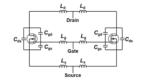
Figure 1. Model equivalent circuit of two MOSFETs connected in parallel 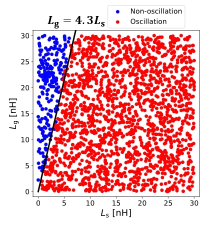
Figure 2. Simulation of oscillation in two MOSFETs with zero gate resistance connected in parallel 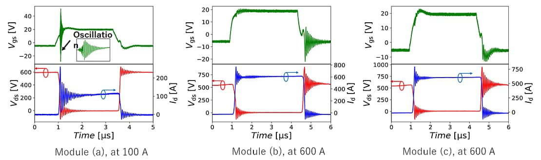
Vgs: Gate-Source voltage, Vds: Drain-Source voltage, Id: Drain current
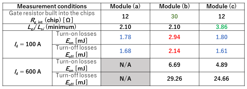
Figure 3. Switching waveforms and switching losses of the prototype modules (Source: Toshiba Group tests) Original – Toshiba
-

MCC introduced the latest additions to its robust portfolio: 10 1200V SiC N-channel MOSFETs in versatile TO-247-4, TO-247-4L, and TO-247AB packages. These new MOSFETs are available in 3-pin and 4-in (Kelvin source) configurations and meet the rising demand for high-power, high-voltage applications.
Boasting exceptional on-resistance values from 21mΩ to 120mΩ (typ.) and fast switching speeds, these components are the ones you can count on for reliable performance. Their excellent thermal properties and fast intrinsic body diode ensure smooth, efficient operation in the most challenging conditions, making them a must-have for critical power systems.
Features & Benefits:
- High-power capability: 1200V MOSFET with SiC technology
- Fast, reliable switching: Intrinsic body diode improves efficiency & ruggedness Enhanced performance: High switching speed with low gate charge
- Wide on-resistance selection: ranging from 21mΩ to 120mΩ (typ.)
- Efficiency: Superior thermal properties and low switching losses
- Durability: Avalanche ruggedness
- Versatility: TO247 3-pin and 4-pin package options
Original – Micro Commercial Components
-

Power Master Semiconductor (PMS) announced the release of its new AEC-Q101 qualified 1200V eSiC MOSFET in a D2PAK-7L package, designed to revolutionize power electronics in electric vehicles (EVs). PMS’s automotive-grade 1200V eSiC MOSFET offers superior efficiency, high power density, high reliability, and enables bi-directional operation, making it an ideal choice for a wide range of automotive applications, including on-board chargers (OBCs), DC-DC converters, and e-compressors.
The automotive industry is rapidly transitioning towards electrification, driven by the growing demand for sustainable and environmentally friendly transportation solutions. This shift has created a surge in demand for high-performance power electronics that can meet the stringent requirements of EV applications. Bi-directional operation is the key trend for the on-board chargers (OBCs) applications to meet V2L (Vehicle to Load), V2G (Vehicle to Grid), V2V (Vehicle to Vehicle), and V2H (Vehicle to Home appliance).
Therefore, the topology of OBCs is moving to Totem-pole PFC + CLLC or DAP resonant converter from Interleaved CCM PFC or Dual boost bridgeless PFC + LLC resonant converters. Larger battery capacity and faster charging demands are driving 800V battery systems for BEV application.
The automotive grade 1200V eSiC MOSFET is an optimized solution for the e-compressor, an indispensable power conversion system for efficient thermal management that increases battery life, charging efficiency, and driving range, and maintains a comfortable environment. It is also optimized for Totem-Pole PFC and CLLC/DAB (Dual Active Bridge) topologies, which are essential for bidirectional power conversion, a key trend in onboard chargers (OBC) for 800V battery system in electric vehicles.
Key Features of automotive grade 1200V e SiC MOSFET
- AEC-Q101 qualified for automotive applications
- Robust Avalanche Capability
- 100% Avalanche Tested
- Operating temperature range : -55°C to +175°C
- Low switching losses
- D2PAK-7L kelvin source package for ease of design and integration
“Driven by our unwavering commitment to innovation and sustainability, Power Master Semiconductor continuously develops power device solutions that achieve breakthrough efficiency and performance”, said Namjin Kim, Senior Director of Sales & Marketing.” The introduction of our new automotive-grade 1200V eSiC MOSFET represents a major leap forward in empowering the automotive industry’s shift towards cleaner, more energy-efficient power electronics. We are confident that this innovative solution will be the optimal choice for high-performance automotive applications.”
Original – Power Master Semiconductor
-

Navitas Semiconductor released its 4.5 kW AI data center power supply reference design, with optimized GaNSafe™ and Gen-3 ‘Fast’ (G3F) SiC power components. The optimized design enables the world’s highest power density with 137 W/in3 and over 97% efficiency.
Next-generation AI GPUs like NVIDIA’s Blackwell B100 and B200 each demand over 1 kW of power for high-power computation, 3x higher than traditional CPUs. These new demands are driving power-per-rack specifications from 30-40 kW up to 100 kW.
Navitas announced its AI Power Roadmap in March 2024, showcasing next-generation data center power solutions for the growing demand in AI and high-performance computing (HPC) systems. The first design was a GaNFast-based 3.2 kW AC-DC converter in the Common Redundant Power Supply (CRPS) form factor, as defined by the hyperscale Open Compute Project. The 3.2 kW CRPS185 (for 185 mm length) enabled a 40% size reduction vs. the equivalent legacy silicon approach and easily exceeded the ‘Titanium Plus’ efficiency benchmark, critical for data center operating models and a requirement for European data center regulations.
Now, the latest 4.5 kW CRPS185 design demonstrates how new GaNSafe™ power ICs and GeneSiC Gen-3 ‘Fast’ (G3F) MOSFETs enables the world’s highest power density and efficiency solution. At the heart of the design is an interleaved CCM totem-pole PFC using SiC with full-bridge LLC topology with GaN, where the fundamental strengths of each semiconductor technology are exploited for the highest frequency, coolest operation, optimized reliability and robustness, and highest power density and efficiency. The 650 V G3F SiC MOSFETs feature ‘trench-assisted planar’ technology which delivers world-leading performance over temperature for the highest system efficiency and reliability in real-world applications.
For the LLC stage, 650 V GaNSafe power ICs are ideal and unique in the industry with integrated power, protection, control, and drive in an easy-to-use, robust, thermally-adept TOLL power package. Additionally, GaNSafe power ICs offer extremely low switching losses, with a transient-voltage capability up to 800 V, and other high-speed advantages such as low gate charge (Qg), output capacitance (COSS), and no reverse-recovery loss (Qrr). High-speed switching reduces the size, weight, and cost of passive components in a power supply, such as transformers, capacitors, and EMI filters. As power density increases, next-gen GaN and SiC enable sustainability benefits, specifically CO2 reductions due to system efficiency increases and ‘dematerialization’.
The 3.2 kW and 4.5 kW platforms have already generated significant market interest with over 30 data center customer projects in development expected to drive millions in GaN and SiC revenue, ramping from 2024 into 2025.
Navitas’ AI data center power supply reference designs dramatically accelerate customer developments, minimize time-to-market, and set new industry benchmarks in energy efficiency, power density and system cost, enabled by GaNFast power ICs and GeneSiC MOSFETs. These system platforms include complete design collateral with fully tested hardware, embedded software, schematics, bills-of-material, layout, simulation, and hardware test results.
“AI is dramatically accelerating power requirements of data centers, processors and anywhere AI is going in the decades to come creating a significant challenge for our industry. Our system design center has stepped up to this challenge delivering a 3x increase in power in less than 18 months”, said Gene Sheridan, CEO of Navitas Semiconductor. “Our latest GaNFast technology, combined with our G3F SiC technology are delivering the highest power density and efficiency the world has ever seen…the perfect solution for the Blackwell AI processors and beyond.”
Original – Navitas Semiconductor
-

onsemi has signed a multi-year deal with Volkswagen Group to be the primary supplier of a complete power box solution as part of its next-generation traction inverter for its Scalable Systems Platform (SSP). The solution features silicon carbide-based technologies in an integrated module that can scale across all power levels – from high power to low power traction inverters to be compatible for all vehicle categories.
“By offering a complete power system solution that encompasses the entire power sub-assembly, we provide Volkswagen Group with a single, simplified modular and scalable platform that maximizes efficiency and performance for their vehicle lineup,” said Hassane El-Khoury, president and CEO of onsemi. “This new approach allows for the customization of power needs and the addition of features for different vehicles without compromising on performance, all while reducing cost.”
Based on the EliteSiC M3e MOSFETs, onsemi’s unique power box solution can handle more power in a smaller package which significantly reduces energy losses. The inclusion of three integrated half-bridge modules mounted on a cooling channel will further improve system efficiency by ensuring heat is effectively managed from the semiconductor to the coolant encasement.
This leads to better performance, improved heat control, and increased efficiency, allowing EVs to drive further on a single charge. By using this integrated solution, Volkswagen Group will be able to easily transition to future EliteSiC-based platforms and remain at the forefront of EV innovation.
“We are very pleased to have onsemi as a strategic supplier for the power box of the traction inverter for our first tranche in the SSP platform. onsemi has convinced us with a deeply verticalized supply chain from the growth of the raw material up to the assembly of the power box,” said Mr. Dirk Große-Loheide, Member of the Extended Executive Committee Group Procurement and Member of the Board Volkswagen Brand for “Procurement”.
Mr. Till von Bothmer, Senior Vice President VW Group Procurement for Powertrain added, “On top of the verticalization, onsemi has furthermore provided a resilient supply concept with regional silicon carbide fabs across Asia, Europe and the U.S. In addition, onsemi will continuously provide the latest SiC generation to ensure competitiveness.
Volkswagen Group will also benefit from onsemi’s planned investment to expand its silicon carbide manufacturing in the Czech Republic. The investment would establish an end-to-end production facility in Europe for the traction inverter power system. The proximity of onsemi’s facility would fortify Volkswagen Group’s supply chain while improving logistics and allowing for faster integration into the manufacturing process.
Original – onsemi
-

Infineon Technologies AG announced that its CoolSiC™ 2000 V modules have been selected by Daihen Corporation for their innovative unit-type power conditioners for grid storage batteries. In the journey towards reducing carbon emissions, both grid storage batteries and the power conditioners that are linked to them play a vital role in facilitating the wider adoption of renewable energy sources like solar and wind power generation.
There has been an increasing demand for higher voltage storage batteries and power conditioners to enhance the effectiveness of power generation, storage, and transmission. Moreover, with the expansion of storage battery systems on a larger scale, finding suitable locations and minimizing construction costs have emerged as significant challenges.
The unit-type power conditioner for grid storage batteries launched by Daihen in March 2024 is the first product in the industry to achieve connection to storage batteries at a high DC link voltage of 1500 V. The higher voltage enables the product to be used with large-capacity storage battery facilities, which has resulted in a 40% reduction in the footprint of grid storage batteries compared to the conventional product.
The high power density is achieved by using Infineon’s 62 mm CoolSiC MOSFET 2000 V module (FF3MR20KM1H). In addition to the characteristics of SiC that enable high voltage, better thermal dissipation and high power density, Infineon’s SiC products feature M1H trench technology that increases the gate drive voltage range and provides high robustness and reliability against gate voltage spikes. Infineon was the pioneer in the industry to introduce the 2000 V class for a SiC module. This innovation has been instrumental in simplifying the inverter circuit configuration. Furthermore, the optimized 62 mm package has led to a substantial reduction in system size, contributing to enhanced efficiency and performance.
Mr. Akihiro Ohori, General Manager, Development Department, Energy Management System Division, Daihen, said, “In order to increase the voltage of power conditioners, the circuit configuration of conventional 1200 V devices had become complicated. However, by adopting Infineon’s 2000 V SiC modules, we were able to achieve a simplified circuit configuration and control design, thereby reducing development resources and the footprint.”
Masanori Fujimori, Marketing Director of the Industrial & Infrastructure Segment at Infineon Technologies Japan, said, “We are very pleased that our pioneering CoolSiC 2000 V module has contributed to the development of the industry’s highest power density power conditioners for grid storage batteries. We believe that Infineon’s SiC technology will address the need for higher efficiency in energy storage systems and will greatly contribute to the growth of renewable energy.”
Original – Infineon Technologies
-

Power Master Semiconductor has released 2nd generation of the 1200V eSiC MOSFET to meet the requirements of higher efficiency, high power density, robust reliability, and ruggedness in various applications such as DC EV charging stations, solar inverters, energy storage systems (ESS), motor drives and industrial power supplies. 1200V eSiC MOSFETs offer significant system advantages such as higher power density, efficiency and less cooling effort due to its much lower power losses.
Therefore, SiC MOSFETs are gaining popularity especially for renewable energy systems, EV charging systems that required higher power density, efficiency and robustness. DC EV charging station is level-3 charger and its power level is increasing by modular configuration as demand of faster charging time and higher battery capacity of EV. DC EV charging provides a mostly constant current output for wide DC output voltage range (200V to 900V) and load profile.
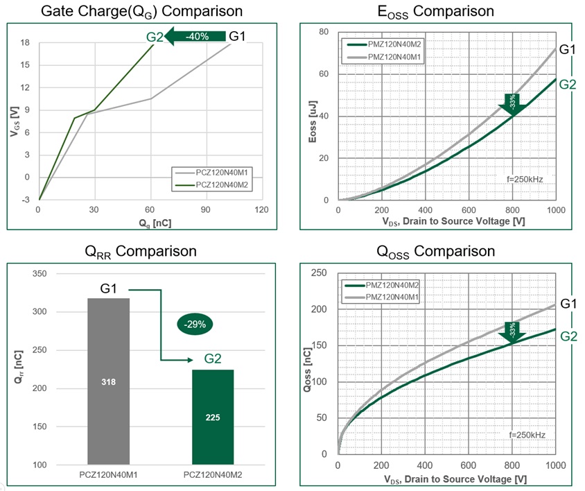
The new generation of 1200V eSiC MOSFET, Gen2 improved key FOM characteristics such as gate charge (QG), stored energy in output capacitance (EOSS), reverse recovery charger (QRR) and output charge (QOSS) by up to 30% compared to previous generation. This new generation SiC MOSFET technology offers significant system advantages such as smaller, lighter, higher efficiency, and less cooling effort thanks to its much lower power losses in various power conversion applications.
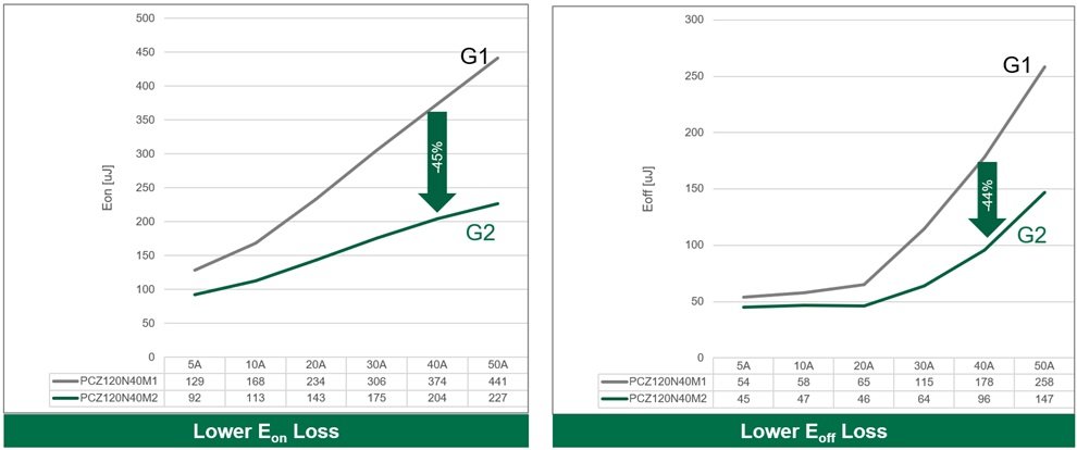
1200V eSiC MOSFET Gen2 offer excellent switching performance and 100% tested avalanche capability. It achieved 44% lower switching loss compared to the previous generation by extremely low miller capacitance (QGD).
Power Master Semiconductor is steadfastly committed to developing cutting-edge power device solutions that prioritize efficiency and sustainability,” said Namjin Kim, Sr. Director Sales & Marketing. “The introduction of our new generation of 1200V eSiC MOSFET marks a substantial leap forward in facilitating the development of cleaner, more efficient power systems. We are confident that the 1200V eSiC Gen2 MOSFET will play a transformative role in high-performance applications.
Original – Power Master Semiconductor
-

In the face of escalating climate crises and a dramatic rise in global energy demands, governments and industries are committing to ambitious climate goals aimed at mitigating environmental impact and securing a sustainable future. Key to these efforts is the transition to electrification to reduce carbon emissions and embrace renewable energy resources.
In a significant step towards accelerating this global transition, onsemi introduced its latest generation silicon carbide technology platform, EliteSiC M3e MOSFETs. The company also disclosed plans to release multiple additional generations through 2030.
“The future of electrification is dependent on advanced power semiconductors. Today’s infrastructure cannot keep up with the world’s demands for more intelligence and electrified mobility without significant innovations in power. This is critical to the ability to achieve global electrification and stop climate change,” said Simon Keeton, group president, Power Solutions Group, onsemi. “We are setting the pace for innovation, with plans to significantly increase power density in our silicon carbide technology roadmap through 2030 to be able to meet the growing demands for energy and enable the global transition to electrification.”
The EliteSiC M3e MOSFETs will play a fundamental role in enabling the performance and reliability of next-generation electrical systems at lower cost per kW, thus influencing the adoption and effectiveness of electrification initiatives. With the ability to operate at higher switching frequencies and voltages while minimizing power conversion losses, this platform is essential for a wide range of automotive and industrial applications such as electric vehicle powertrains, DC fast chargers, solar inverters and energy storage solutions.
Additionally, the EliteSiC M3e MOSFETs will enable the transition to more efficient, higher-power data centers to meet the exponentially increasing energy demands that power a sustainable artificial intelligence engine.
Through onsemi’s unique design engineering and manufacturing capabilities, the EliteSiC M3e MOSFETs achieve a significant reduction in both conduction and switching losses on the trusted and field-proven planar architecture. Compared to previous generations, the platform can reduce conduction losses by 30% and turn-off losses by up to 50%.
By extending the life of SiC planar MOSFETs and delivering industry-leading performance with EliteSiC M3e technology, onsemi can ensure the robustness and stability of the platform, making it a preferred choice for critical electrification applications
The EliteSiC M3e MOSFETs also offer the industry’s lowest specific on-resistance (RSP) with short circuit capability which is critical for the traction inverter market that dominates SiC volume. Packaged in onsemi’s state-of-the-art discrete and power modules, the 1200V M3e die delivers substantially more phase current than previous EliteSiC technology, resulting in approximately 20% more output power in the same traction inverter housing. Conversely, a fixed power level can now be designed with 20% less SiC content, saving costs while enabling the design of smaller, lighter and more reliable systems.
Additionally, onsemi provides a broader portfolio of intelligent power technologies including gate drivers, DC-DC converters, e-Fuses and more to pair with the EliteSiC M3e platform. The end-end onsemi combination of optimized, co-engineered power switches, drivers and controllers enable advanced features via integration, lowering overall system cost.
Global energy demands are projected to soar over the next decade, making the need for increased power density in semiconductors paramount. onsemi is leading innovation across its silicon carbide roadmap – from die architectures to novel packaging techniques – that will continue to address the general industry demand for increased power density.
With each new generation of silicon carbide, cell structures will be optimized to efficiently push more current through a smaller area, increasing power density. When coupled with the company’s advanced packaging techniques, onsemi will be able to maximize performance and reduce package size.
By applying the concepts of Moore’s Law to the development of silicon carbide, onsemi can develop multiple generations in parallel and accelerate its roadmap to bring several new EliteSiC products to market at an accelerated pace through 2030.
“We are applying our decades of experience in power semiconductors to push the boundaries of speed and innovation in our engineering and manufacturing capabilities to meet the rising global energy demands,” said Dr. Mrinal Das, senior director of technical marketing, Power Solutions Group, onsemi. “There is a huge technical interdependency between the materials, device and package in silicon carbide. Having full ownership over these key aspects allows us to have control over the design and manufacturing process and bring new generations to market much faster.”
The EliteSiC M3e MOSFET in the industry-standard TO-247-4L package is now sampling.
Original – onsemi
-

AIXTRON SE supports Nexperia B.V. in the ramp-up of its 200mm volume production for silicon carbide (SiC) and gallium nitride (GaN) power devices. With the new G10-SiC for the 200mm SiC volume ramp, Nexperia is placing a repeat order for AIXTRON SiC tools. This is complemented by an order for AIXTRON G10-GaN tools.
Both GaN and SiC epitaxial films are essential for the design of next-generation energy-efficient Field-Effect (FET) or Metal-Oxide-Field Effect (MOSFET) transistors to be used in various power conversion applications ranging from data centers and solar inverters in electric vehicles (EV) or trains.
Nexperia has decades of experience in the development of power devices, achieving more than 2.1 billion USD in revenue in 2023. After releasing its first GaN FET device in 2019 and its first SiC MOSFET in 2023, Nexperia continues to expand its portfolio with new high-reliability and power-efficient devices.
Nexperia, headquartered in Nijmegen (Netherlands), operates front-end factories in Hamburg (Germany) and Greater Manchester (England). The AIXTRON epitaxy systems will be installed at Nexperia’s wafer fab in Hamburg (Germany), further strengthening the semiconductor production capabilities in the region. Nexperia’s Hamburg site produces approximately 100 billion discrete semiconductors annually, accounting for about a quarter of the global production of this type of products.
“We are honored to strengthen our alliance with Nexperia, a pivotal player in the semiconductor landscape. Our G10 epitaxy solutions are at the heart of this collaboration, bolstering Nexperia’s growth strategies and enabling the high-volume production of wide bandgap semiconductors for commercial applications. Together, we are setting the pace for the industry’s transition to more energy-efficient SiC and GaN solutions”, said Dr. Felix Grawert, CEO and President of AIXTRON SE.
“As we advance our technological capabilities and market presence in high-power semiconductor production, our strategic partnership with AIXTRON is transformative. Integrating the G10 systems will significantly enhance our wide bandgap technology development and production capabilities. We build on AIXTRON’s proven uniformity and leverage the additional productivity gains of AIXTRON’s G10 tools to scale up our production efficiently and cost-effectively. With the new G10 tools in our Hamburg facility, we are poised for further advancements in our production capabilities,” said Achim Kempe, COO at Nexperia B.V.
Original – AIXTRON
