-
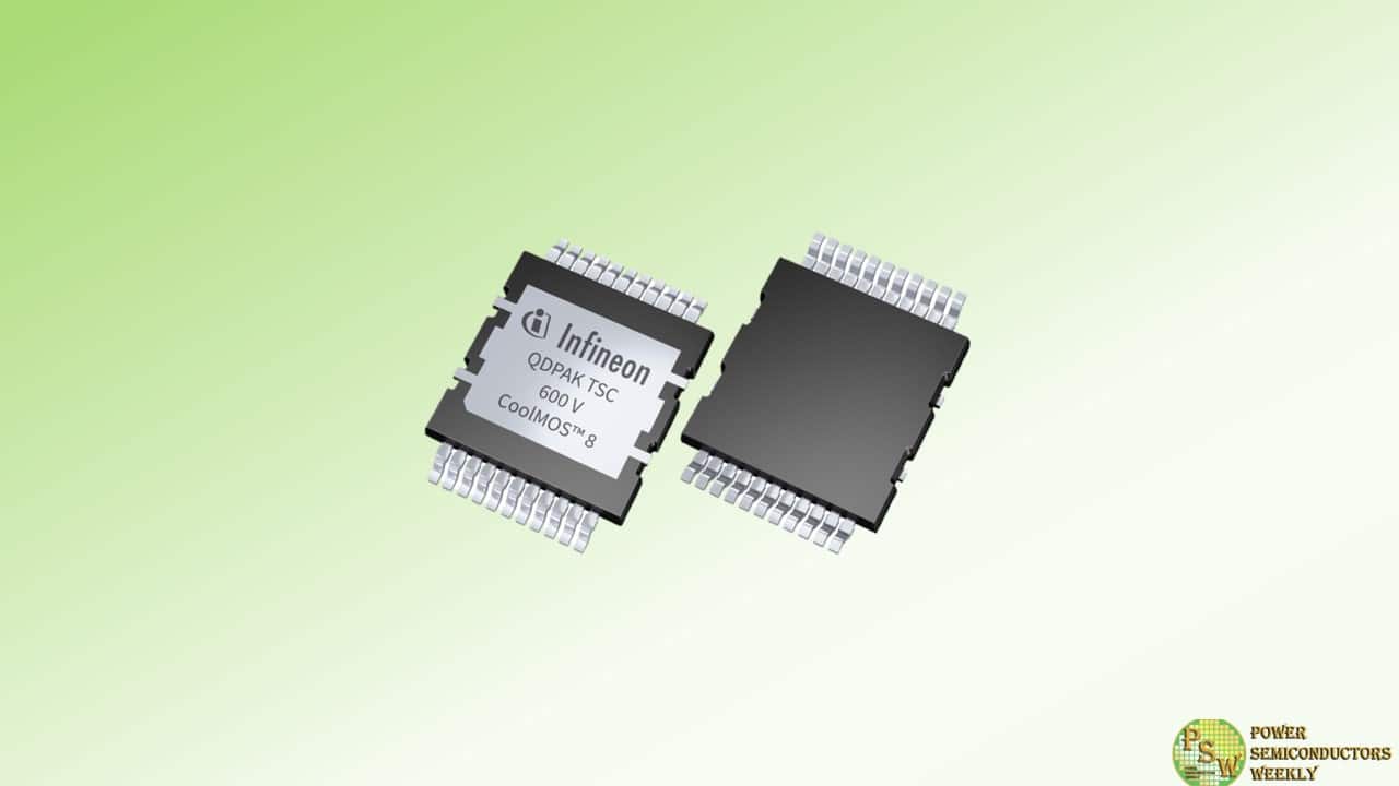
Infineon Technologies AG introduced the 600 V CoolMOS™ 8 high voltage superjunction (SJ) MOSFET product family. The devices combine the best features of the 600 V CoolMOS 7 MOSFET series and are the successors to the P7, PFD7, C7, CFD7, G7 and S7 product families. The new superjunction MOSFETs enable cost-effective Si-based solutions that enhance Infineon’s wide-bandgap offering. They are equipped with an integrated fast body diode, making them suitable for a wide range of applications such as server and industrial switched-mode power supply units (SMPS), EV chargers, and micro-solar.
The components come in SMD QDPAK, TOLL and ThinTOLL 8 x 8 packages, which simplifies designs and reduces assembly costs. At 10 V, the 600 V CoolMOS 8 SJ MOSFETs offer 18 percent lower gate charge (Q g) than the CFD7 and 33 percent lower than the P7. At 400 V, the product family offers a 50 percent lower output capacitance C OSS than the CFD7 and the P7.
In addition, the turn-off losses (E oss) have been reduced by 12 percent compared to the CFD7 and the P7 and the reverse recovery charge (Q rr) is 3 percent lower compared to the CFD7. Furthermore, the devices offer the lowest reverse recovery time (t rr) on the market and the thermal performance has been improved by 14 to 42 percent compared to the previous generation.
With these features, the devices offer high efficiency and reliability in soft-switching topologies such as LLC and ZVS phase-shift full-bridge. They also provide excellent performance levels in PFC, TTF and other hard-switching topologies. Due to their optimized R DS(on), the devices offer higher power density, allowing products in a Si-based super junction (SJ) technology to be reduced to a single-digit value of 7 mΩ.
Infineon will showcase the 600 V CoolMOS 8 SJ MOSFETs at the Infineon booth (Hall 7 / Booth 470) at PCIM 2024 in Nuremberg. Samples of the 600 V CoolMOS 8 SJ MOSFETs are now available. More information is at www.infineon.com/coolmos8.
Original – Infineon Technologies
-
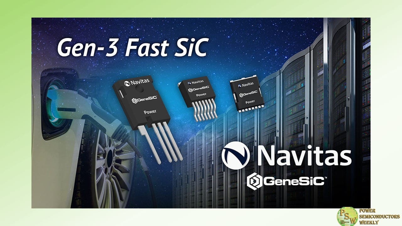
Navitas Semiconductor announced their new portfolio of Gen-3 ‘Fast’ (G3F) 650 V and 1,200 V SiC MOSFETs optimized for fastest switching speed, highest efficiency, and increased power density for applications such as AI data center power supplies, on-board chargers (OBCs), fast EV roadside super-chargers, and solar / energy-storage systems (ESS). The broad portfolio range covers industry-standard packages from D2PAK-7 to TO-247-4, designed for demanding, high-power, high-reliability applications.
The G3F family is optimized for high-speed switching performance, resulting in 40% improvement to hard-switching figures-of-merits (FOMs) compared to competition in CCM TPPFC systems. This will enable increasing the wattage of next-generation AI power supply units (PSUs) up to 10 kW, and power per rack increase from 30 kW to 100-120 kW.
The G3F GeneSiC MOSFETs are developed using a proprietary ‘trench-assisted planar’ technology. and offer better-than-trench MOSFET performance, while also providing superior robustness, manufacturability and cost than competition. G3F MOSFETs deliver high-efficiency with high-speed performance, enabling up to 25°C lower case temperature, and up to 3x longer life than SiC products from other vendors.
The ‘trench-assisted planar’ technology enables an extremely low RDS(ON) increase versus temperature, which results in the lowest power losses across the complete operating range and offers up to 20% lower RDS(ON) under real-life operation at high temperatures compared to competition.
Additionally, all GeneSiC MOSFETs have the highest-published 100%-tested avalanche capability, 30% longer short-circuit withstand time, and tight threshold voltage distributions for easy paralleling, GeneSiC MOSFETs are ideal for high-power, fast-time-to-market applications.
Navitas’ latest 4.5 kW high-power density AI Server PSU reference design in CRPS185 form-factor, showcases the 650 V-rated, 40mOhms G3F FETs for an Interleaved CCM TP PFC topology. Alongside the GaNSafe™ Power ICs in the LLC stage, a power density of 138 W/inch3 and peak efficiency above 97% is realized, which comfortably achieves ‘Titanium Plus’ efficiency standards, now mandatory in Europe.
For the EV market, 1,200 V/34 mOhm (G3F34MT12K) G3F FETs enable Navitas’ new 22 kW, 800V Bi-Directional OBC and 3KW DC-DC converter to achieve a superior power density of 3,5 kW/L and a peak efficiency of 95.5%.
“G3F sets a new standard for efficient, cool-running SiC performance, coupled with high reliability and robustness for high-power, high-stress systems,” noted Dr. Sid Sundaresan, Senior Vice President of SiC Technology and Operations. “We’re pushing the boundaries of SiC, with up to 600 kHz switching speeds, and hard-switching figures-of-merit up to 40% better than competition.”
Original – Navitas Semiconductor
-

Alpha and Omega Semiconductor Limited announced the expansion of their package portfolio options available for their second generation 650V to 1200V αSiC MOSFETs. Applicable to many critical applications such as xEV charging, solar inverters, and industrial power supplies, the new package selections give designers the added flexibility of multiple system optimization options to further maximize system efficiency while streamlining their manufacturing process.
AOS will showcase its expanded surface mount and module package options at PCIM Europe 2024 in Nuremberg, Germany, June 11-13.
The first new surface mount package is available for the AOBB040V120X2Q, AOS’ new 1200V/40mOhm αSiC MOSFET in a standard D2PAK-7L surface mount package. This AEC-Q101 qualified product is designed to replace traditional through-hole packages. It is ideal for applications such as on-board chargers (OBCs) where efficient cooling can be provided by vias and backside PCB heatsinks, simplifying the assembly flow and maximizing the power density. In addition, the low inductance package combined with the fast driver sourcesense connection positions these AOS αSiC MOSFETs as one of the most efficient power-switching solutions in the market.
For additional design flexibility, AOS is releasing its GTPAK™ surface mount package with topside cooling features. In designs where a topside-mounted heatsink is viable, the direct heat path from the GTPAK minimizes the thermal resistance. It enables higher power dissipation for more effective PCB routing. The first AOS product in GTPAK is the AOGT020V120X2. This 1200V/20mOhm αSiC MOSFET is an ideal solution to meet the requirements of high-efficiency solar inverter and industrial power supply applications.
Finally, AOS announced the AOH010V120AM2 as the first product in its new AlphaModule™ high power baseplate-less module family. This 1200V/10mOhm half-bridge αSiC module features press-fit pins and an integrated thermistor. It is in a standard footprint module that enables the replacement of multiple discrete devices into a single compact form factor while simplifying both the mechanical and electrical design by providing a clear separation of electrical and cooling paths. Single modules are suitable for residential solar inverters, or several modules in parallel will allow scaling to power levels necessary to drive the needs of fast DC charging stations.
“With the continued growth in EVs, energy infrastructure, and renewable energy, we continue to see increased interest in our αSiC MOSFETs. The expansion of our product portfolio to include these new advanced package options gives our customers the design flexibility they need to take advantage of our superior αSiC performance and continue the trend of pushing power systems to higher density and efficiency,” said David Sheridan, Vice President of SiC products at AOS.
Original – Alpha and Omega Semiconductor
-
Vincotech introduced a GaN-based power module which provides an effective solution for highly efficient power conversion in isolated DC/DC converters or DC/AC inverter stages. It offers a 2-in-1 solution, and can be utilized either as a 10mOhm H-Bridge or 5mOhm half-bridge.
The module features E-mode GaN HEMTs chip technology, promoting high efficiency and power density, and is available in an industry-standard package with low stray loop inductance. It is compatible with external gate drives, offering engineers high design flexibility.
Main benefits
- Highest design flexibility with external gate driver, enabling slew rate control for low EMC
- Low voltage overshoots due to integrated snubber capacitors
- High power density and small footprint for soft switching above 500kHz
- Kelvin source pin and low inductive gate loop for clean switching behavior
Applications
- DC fast charger
- Solar inverter
- UPS
Original – Vincotech
-
Semikron Danfoss and Vincotech announced the renewal of their cooperation agreement for power semiconductor module packaging. The two enterprise’s alliance, dating back to 2003, has been extended to further strengthen MiniSKiiP packaging technology.
This move underscores Semikron Danfoss and Vincotech’s commitment to advancing MiniSKiiP and delivering cutting-edge solutions that meet the needs of the power electronics industry.
“The partnership with Vincotech is key to ensuring the safe supply of our number one motor drive module MiniSKiiP to our customers,” said Peter Sontheimer, Senior Vice President Industry Division at Semikron Danfoss. “We strongly believe that this type of arrangement is beneficial to the long-term health of the power electronics supply chain.”
Multiple source options for the package to further mitigate the supply chain risk, as well as standards-compliant design, are just a few of the benefits of this renewed cooperation agreement. Engineered for easy assembly and featuring service-friendly spring contacts, MiniSKiiP’s unique hardware has earned an excellent reputation for efficiency and performance in general purpose and servo motor drives.
“We are delighted to be renewing our partnership with Semikron Danfoss for the MiniSKiiP package technology,” said Edoardo Guiotto, VP Sales & Marketing at Vincotech. “This agreement reaffirms our dedication to deliver premium products to our customers and drive innovation and advances in power electronics.”
Semikron Danfoss and Vincotech are now set to take MiniSKiiP’s reliability and standardization to the next level. Customers can look forward this technology bringing even greater robustness, versatility, and compatibility to their products.
Original – Semikron Danfoss
-

As data centers become increasingly power-hungry to support the tremendous processing requirements of AI workloads, the need for boosting energy efficiency is paramount. The powerful combination of onsemi’s latest generation T10 PowerTrench® family and EliteSiC 650V MOSFETs create a solution that offers unparalleled efficiency and high thermal performance in a smaller footprint for data center applications.
Compared to a typical search engine request, an AI-supported engine request requires more than 10x the power, leading to data center power needs expected to reach an estimated 1,000 TWh globally in less than two years. To process one AI-supported request, energy is converted four times from the grid to the processor, which can result in an energy loss of approximately 12%.
Using the T10 PowerTrench family and EliteSiC 650V solution, data centers are able to reduce power losses that occur by an estimated 1%. If implemented in data centers globally, the solution could reduce energy consumption by 10 TWh annually or the equivalent of the energy required to fully power nearly one million homes per year.
The EliteSiC 650V MOSFET offers superior switching performance and lower device capacitances to achieve higher efficiency in data centers and energy storage systems. Compared to the previous generation, these new generation silicon carbide (SiC) MOSFETs have halved the gate charge and reduced both the energy stored in output capacitance (Eoss) and the output charge (Qoss) by 44%.
With no tail current during turn-off and superior performance at high temperatures, they can also significantly reduce switching losses compared to super junction (SJ) MOSFETs. This allows customers to downsize system components while increasing the operating frequency, resulting in an overall reduction in system costs.
Separately, the T10 PowerTrench Family is engineered to handle high currents, crucial for DC-DC power conversion stages, and offers increased power density and superior thermal performance in a compact footprint. This is achieved through a shield gate trench design, which boasts an ultra-low gate charge and an RDS (on) of less than 1 milliohm. Additionally, the soft recovery body diode and lower Qrr effectively minimizes ringing, overshoots, and electrical noise to ensure optimal performance, reliability, and robustness under stress. The T10 PowerTrench Family also meets the stringent standards required for automotive applications.
The combined solution also meets the stringent Open Rack V3 (ORV3) base specification required by hyperscale operators to support the next generation of high-power processors.
“AI and electrification are reshaping our world and skyrocketing power demands. Accelerating innovation in power semiconductors to improve energy efficiency is key to enabling these technological megatrends. This is how we power the future responsibly,” said Simon Keeton, group president, Power Solutions Group, onsemi. “Our latest solution can significantly reduce power losses that occur during the energy conversion process and have a meaningful impact on the demands for the next generation of data centers.”
Original – onsemi
-

Vanguard International Semiconductor Corporation and NXP Semiconductors N.V. announced the plan to create a manufacturing joint-venture VisionPower Semiconductor Manufacturing Company Pte Ltd (“VSMC”) which will build a new 300mm semiconductor wafer manufacturing facility in Singapore.
The joint-venture fab will support 130nm to 40nm mixed-signal, power management and analog products, targeting the automotive, industrial, consumer and mobile end markets. The underlying process technologies are planned to be licensed and transferred to the joint venture from TSMC.
The joint venture will begin construction of the initial phase of the wafer fab in the second half of 2024, pending receipt of all required regulatory approvals, with initial production available to customers during 2027. The joint venture will operate as an independent, commercial foundry supplier, providing assured proportional capacity to both equity partners, with an expected output of 55,000 300mm wafers per month in 2029. The joint venture will create approximately 1,500 jobs in Singapore. Upon the successful ramp of the initial phase, a second phase will be considered and developed pending commitments by both equity partners.
The total cost of the initial build out is anticipated to be $7.8 billion. VIS will inject $2.4 billion representing a 60 percent equity position in the joint venture and NXP will inject $1.6 billion for the remaining 40 percent equity position. VIS and NXP have agreed to contribute an additional $1.9 billion which will be utilized to support the long-term capacity infrastructure. The remaining funding including loans will be provided by third parties to the joint venture. The fab will be operated by VIS.
“VIS is pleased to work with leading global semiconductor company NXP to build our first 300mm fab. This project aligns with our long-term development strategies, demonstrating VIS’ commitment to meeting customer demands, and diversifying our manufacturing capabilities,” said VIS Chairman Leuh Fang. “Adhering to the vision of business sustainability, this fab will be built adopting the Singapore Green Mark standards and implementing rigorous green manufacturing measures. We will continue to create great value for our stakeholders and look forward to working with customers, suppliers, local talents, and government to continuously contribute to Singapore and the global semiconductor ecosystem.”
“NXP continues to take proactive actions to ensure it has a manufacturing base which provides competitive cost, supply control, and geographic resilience to support our long-term growth objectives,” said Kurt Sievers, NXP President and CEO. “We believe VIS is well suited and fully understands the complexities involved in building and operating together with NXP a 300mm analog mixed signal fab. The joint venture partnership we intend to create with VIS perfectly aligns within NXP’s hybrid manufacturing strategy.”
Original – NXP Semiconductors
-

Toshiba Electronic Devices & Storage Corporation has started mass production of a 3rd generation silicon carbide (SiC) 1200 V and drain current (DC) rating 400 A of SiC MOSFET module “MG400Q2YMS3” for industrial equipment and has expanded its lineup.
The new product MG400Q2YMS3 offers low conduction loss with low drain-source on-voltage (sense) of 0.9 V (typ.). It also offers low switching loss with both turn-on switching loss and turn-off switching loss of 13 mJ (typ.). These help to reduce power loss of equipment and the size of cooling device.
MG400Q2YMS3 has a low stray inductance of 12 nH (typ.) and is capable of high-speed switching. In addition, it suppresses surge voltage in switching operation. Thus, it is available for high frequency isolated DC-DC converter.
Toshiba’s SiC MOSFET module of 2-153A1A package has a lineup of five existing products, MG250YD2YMS3 (2200 V / 250 A), MG400V2YMS3 (1700 V / 400 A), MG250V2YMS3 (1700 V / 250 A), and MG600Q2YMS3 (1200 V / 600 A), including new products. This provides a wider range of product selection.
Toshiba will continue to meet the needs for high efficiency and the downsizing of industrial equipment.
Applications
Industrial equipment
- Auxiliary power supply for railway vehicles
- Renewable energy power generation systems
- Motor control equipment for industrial equipment
- High frequency DC-DC converters, etc.
Features
- Low drain-source on-voltage (sense):
VDS(on)sense=0.9 V (typ.) (ID=400 A, VGS=+20 V, Tch=25 °C) - Low turn-on switching loss:
Eon=13 mJ (typ.) (VDD=600 V, ID=400 A, Tch=150 °C) - Low turn-off switching loss:
Eoff=13 mJ (typ.) (VDD=600 V, ID=400 A, Tch=150 °C) - Low stray inductance:
LsPN=12 nH (typ.)
Original – Toshiba
-

ElevATE Semiconductor and GlobalFoundries announced a manufacturing partnership for high-voltage chips produced at GF’s facility in Essex Junction, Vermont. Designed by ElevATE and manufactured at scale by GF on its proven and power-efficient 7HV technology platform, the chips are vital to both commercial semiconductor testing equipment and critical applications for aerospace and defense systems.
The agreement outlines GF’s supply of its 7HV chip technology to ElevATE and the marketplace. Manufactured on 200mm wafers at GF’s Vermont facility, the mature-node chips pair power management and wireless sensing capabilities, delivering the performance, design flexibility and power efficiency required by a range of electronics devices in national security systems. The 7HV platform is optimized for cost and performance, and offers a full suite of features and options with well-characterized design tools, as well as proven manufacturing reliability with robust yields.
To meet the demands of commercial clients and the aerospace and defense industry, ElevATE and GF are collaborating to provide restart support and reestablish the production of 7HV chips. The renewed availability of the 7HV platform will save customers costs, time, and the challenge of redesigning their products using a different chip technology. The new supply will build upon the success of the millions of 7HV chips previously manufactured at GF’s Vermont facility.
“This collaboration marks a significant transformation in ElevATE’s production strategy, transitioning its fabrication processes to GlobalFoundries,” said Anil Kodali, Vice President of Operations and Quality Assurance at ElevATE. “With GF as our manufacturing partner, we can be sure of a robust and reliable source of supply, enabling us to meet the escalating demands of our customers in terms of volume, quality and time-to-market.”
“Our collaboration with ElevATE underscores GF’s commitment to ensuring the U.S. semiconductor and national security ecosystems have a reliable supply of secure, domestically manufactured chips,” said Nicholas Sergeant, vice president and head of the aerospace, defense and critical infrastructure business at GF. “As the leading supplier of essential chips for the U.S. aerospace and defense industry and a longstanding partner to the Department of Defense, GF goes above and beyond to ensure our national security customers have the chips they need, manufactured where they want them, with the right level of security.”
GF’s facility in Essex Junction, Vermont, near Burlington, was among the first major semiconductor manufacturing sites in the United States. Today, around 1,800 GF employees work at the site. Built on GF’s differentiated technologies, these GF-made chips are used in smartphones, automobiles, and communications infrastructure applications around the world. The facility is a DMEA-accredited Trusted Foundry and manufactures secure chips in partnership with the U.S. government.
Original – GlobalFoundries
-
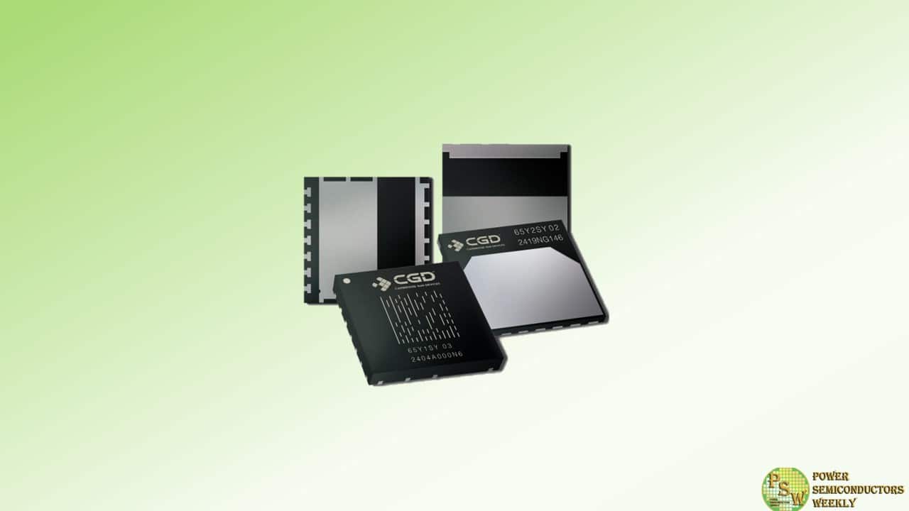
Cambridge GaN Devices (CGD) announced two new packages for the company’s ICeGaN™ family of GaN power ICs that offer enhanced thermal performance and simplify inspection. Variants of the well-proven DFN style, both packages are extremely rugged and reliable.
Developed for CGD, the DHDFN-9-1 (Dual Heat-spreader DFN) is a thin, dual-side cooled package with a small, 10×10 mm footprint and wettable flanks to simplify optical inspection. It offers low thermal resistance (Rth(JC), and can be operated with bottom-side, top-side and dual-side cooling, offering flexibility in design and out-performing the often-used TOLT package in top-side and, especially, dual-side cooled configurations.
The DHDFN-9-1 package has been designed with dual-gate pinout to facilitate optimal PCB layout and simple paralleling, enabling customers to address applications up to 6 kW with ease. The BHDFN-9-1 (Bottom Heat-spreader DFN) is a bottom-side cooled package, also with wettable flanks for easy inspection. Thermal resistance is 0.28 K/W, matching or exceeding other leading devices. Measuring 10×10 mm, the BHDFN is smaller than the commonly-used TOLL package yet shares a similar footprint, hence a common layout with TOLL-packaged GaN power ICs is possible for ease of use and evaluation.
Nare Gabrielyan | Product Marketing Manager, CGD
“These new packages are part of our strategy to enable customers to use our ICeGaN GaN power ICs at higher power levels. Servers, data centres, inverters/motor drives, micro-inverters and other industrial applications are all beginning to enjoy the power density and efficiency benefits that GaN brings, but they are also more demanding. Therefore, it is essential for such applications that devices are also rugged and reliable, and easy to design in. These attributes are inherent in ICeGaN, and are supported and extended by the new packages.”
Improving thermal resistance performance has several benefits. First, more power output is available at the same RDS(on) . Devices also run at cooler temperatures for the same power, so less heatsinking is required, resulting in reduced system costs. Lower operating temperatures also lead to higher reliability and longer lifetimes. Finally, if cost is the constraint for the application, designers can use a lower cost part with a higher RDS(on) and still achieve the required power output.
The new packages will be shown for the first time publicly at the upcoming PCIM exhibition on CGD’s booth # 7 643, Nürnberg Messe, Nuremberg, Germany, 11-13th June 2024.
Original – Cambridge GaN Devices
