-

Qorvo® will showcase its latest power management innovations at the upcoming Applied Power Electronics Conference (APEC) from Feb. 26-28, at the Long Beach Convention Center in California. Attendees are invited to visit the Qorvo booth #1857 to explore the latest advancements in SPICE simulation, silicon carbide (SiC) and battery management technologies.
Qorvo will feature the following highlights at APEC 2024:
QSPICE™ Simulation Software Showcase
APEC attendees can experience the next level of simulation with Qorvo’s advanced QSPICE tool during three insightful training sessions and engage in a Q&A with the tool’s creator, Mike Engelhardt. For those unable to attend APEC, the sessions will be available on the Qorvo YouTube channel in March.Training Session Schedule:
- Tuesday, Feb. 27, 10-10:20 a.m.: The QSPICE User-Interface
- Tuesday, Feb. 27, 3-3:20 p.m.: Importing 3rd Party Models
- Wednesday, Feb. 28, 10-10:20 a.m.: Anatomy of a Macro Model Done Right
Launch of Inaugural SiC Module Family
Qorvo will unveil its first SiC module family, featuring an innovative cascode JFET architecture. This highly integrated device family simplifies high-voltage designs and offers exceptional thermal and electrical performance due to low switching losses, low thermal resistance and RDS(on) as low as 9.4mΩ.Battery Management Demonstrations
Visitors to the booth can see Qorvo’s wireless battery management debut with a demonstration showcasing a remote battery pack monitoring and state of charge solution, created in combination with Qorvo’s IoT microcontroller.Original – Qorvo
-
Micro Commercial Components announced two-in-one IGBT module, MIF400R065C2TL-BP. Available in the C2 package, this new cutting-edge module combines dual IGBT devices and sets the standard for rugged performance. With 650V capability and an ultra-fast and soft recovery anti-parallel rectifier, this module delivers exceptional reliability in high-power applications.
MCC’s IGBT module is a no-brainer for motor controls, uninterruptible power supplies, welding equipment, and other power-intensive applications, thanks to its ability to withstand junction temperatures up to 175°C and a high short-circuit capability of 6us.
Designed with low VCE(sat), IGBT trench technology, and a 400A current rating, this component ensures low switching losses and low inductance while maximizing efficiency.
Features & Benefits:
- Low VCE(sat) with positive temperature coefficient
- Trench IGBT technology
- Low switching losses
- High short-circuit capability (6us)
- Ultra-fast and soft recovery anti-parallel forward diode (FWD)
- Low inductance
- Maximum junction temperature of 175°C
- C2 package
Original – Micro Commercial Components
-
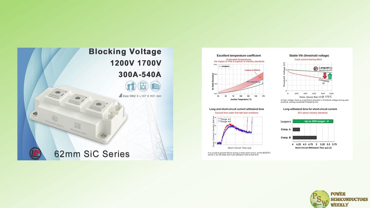
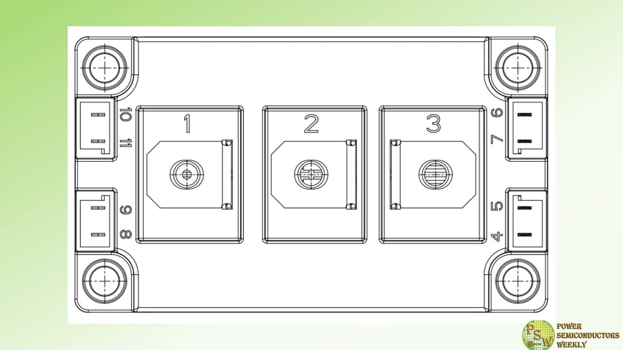
Leapers Semiconductor introduced a new 62 mm package SiC module product portfolio, achieving top-tier performance in the industry. The modules adopt the widely used 62 mm module half-bridge topology design in the industrial field, using high-quality mature chips. It boasts high voltage resistance, outstanding power density, high short-circuit tolerance, and a temperature coefficient 1.4 times better than industry standards.
The 62 mm SiC modules include voltage resistance specifications of 1200V and 1700V, meeting the demands of high-power applications, especially suitable for applications in the smart grid, rail transit, energy storage, and power supplies.
Because of the use of leading-edge chip solutions in the industry and the application of low thermal resistance and low stray capacitance packaging technology, along with the use of Si3N4 AMB low thermal resistance substrate, Leapers’ 62 mm SiC product excels in power density, short-circuit current withstand capability, thermal resistance, and other capabilities. Particularly under high junction temperature conditions, the module’s conduction and switching losses significantly outperform industry standards.
Technical Features:- Voltage resistance options: 1200V or 1700V
- Outstanding current output capability
- Temperature coefficient index better than industry standards
- Low losses, excellent short-circuit current withstand capability
- Si3N4 AMB, low thermal resistance
Currently, Leapers 62 mm SiC modules have undergone bench tests and received orders, involving applications such as grid inverters and auxiliary inverters for rail transit vehicles. Downstream customers include domestic power grid and overseas rail transit enterprises.Original – Leapers Semiconductor
-

Infineon Technologies AG announced that Infineon and Honda Motor Co., Ltd. have signed a Memorandum of Understanding (MoU) to build a strategic collaboration. Honda selects Infineon as semiconductor partner to align future product and technology roadmaps.
The two companies also agreed to continue discussions on supply stability, as well as to encourage transferring mutual knowledge and collaborate on projects aimed at accelerating the time to market of technologies.
“Infineon’s system understanding, our broad product portfolio and outstanding quality have made us an appreciated partner to Japan’s automotive industry,” said Peter Schiefer, President of the Automotive Division at Infineon. “We are honored to be the semiconductor partner for a strategic collaboration with Honda. Intensifying a long-standing partnership even further is always a confirmation of the added value created and at the same time an expression of the trust in contributing to future successes.”
Infineon will support Honda with technologies to enable competitive and advanced vehicles. The technical support will focus on the area of power semiconductors, Advanced Driver Assistance Systems (ADAS), and E/E architectures, where both parties will collaborate on new architecture concepts.
Original – Infineon Technologies
-

Wolfspeed, Inc. announced the expansion of an existing long-term silicon carbide wafer supply agreement with a leading global semiconductor company. The expanded agreement, which is now worth approximately $275 million in total, calls for Wolfspeed to supply the company with 150mm silicon carbide bare and epitaxial wafers, reinforcing both companies’ visions for an industry-wide transition from silicon to silicon carbide semiconductor power devices.
“As the global leader in silicon carbide wafer production, Wolfspeed is uniquely positioned to be a critical supplier of high-quality and advanced silicon carbide materials at scale. We will continue to be an important partner to power device manufacturers who need the highest-quality silicon carbide wafers to service their customers,” said Dr. Cengiz Balkas, SVP and GM of Materials for Wolfspeed.
“This agreement further strengthens our long-time partnership with a best-in-class power semiconductor manufacturer. Our collective efforts are helping to address the rapidly expanding opportunity for silicon carbide and better address the unfulfilled demand that exists in the marketplace today.”
The adoption of silicon carbide-based power solutions is rapidly growing across multiple markets, including industrial and EVs. Silicon carbide solutions enable smaller, lighter and more cost-effective designs, converting energy more efficiently to unlock new applications in electrification. This supply agreement will enable silicon carbide applications in a broad range of industries, such as: renewable energy and storage, electric vehicles, charging infrastructure, industrial power supplies, traction and variable speed drives.
Wolfspeed is the global leader in the manufacturing of silicon carbide wafers and epitaxial wafers. The company is currently expanding its manufacturing capacity in the United States and has plans to open a new, automated materials factory in Siler City, North Carolina later this year that will produce 200mm silicon carbide wafers. The new materials factory will increase Wolfspeed’s current materials production capacity by ten times.
Original – Wolfspeed
-

PANJIT introduced new P-channel and N-channel MOSFETs designed to boost automotive electronic systems. The P-channel MOSFETs, with AEC-Q101 qualification and a high 175°C junction temperature, offer optimal choices for design engineers seeking reliability and simplified circuitry. These MOSFETs, minimizing RDS(ON) and maximizing avalanche ruggedness, are available in flexible packages (DFN3333-8L, DFN5060-8L, DFN5060B-8L, TO-252AA, TO-263, and TO-263-7L).
PANJIT’s N-channel power MOSFETs employ advanced trench technology, delivering excellent figure of merit (FOM), lower RDS(ON), and capacitance. Available in low-profile packages (DFN3333-8L, DFN5060-8L, DFN5060B-8L, TO-252AA), these MOSFETs contribute to efficient and reliable PCB layouts.
By combining innovation with reliability, PANJIT’s low voltage MOSFETs simplify power design circuitry, addressing the evolving needs of automotive design engineers.These components are a testament to PANJIT’s commitment to shaping the future of automotive electronics, offering optimal solutions for high-performance automotive applications.
Key Features of 30V & 40V Automotive-Grade P-Channel MOSFET:
• P-channel enhancement mode logic level MOSFETs
• Low RDS(ON) to minimize conduction losses
• Package with low thermal resistance
• 100% unclamped inductive switching (UIS) tested
• Electrostatic sensitive device (ESD) capable
• AEC-Q101 qualified and PPAP capable
• 175°C operating junction temperature
• Available in TO-263-7L PackageKey Features of 30V & 40V Automotive-Grade N-Channel MOSFET:
• 30V & 40V N-channel advanced trench
• Low RDS(ON) to minimize conduction losses
• Low FOM to minimize driver losses
• Standard and logic level available
• AEC-Q101 qualified and PPAP capable
• 175°C operating junction temperatureOriginal – PANJIT International
-

Moov, the largest and fastest-growing global marketplace for used semiconductor equipment, announced the release of its new Equipment Management Software (EMS) for semiconductor manufacturers. Moov’s Equipment Management Software helps manufacturers track and understand what equipment assets they own across fabrication centers (fabs), the condition of these tools, and the resale value of these assets based on data from Moov’s global marketplace.
Today, semiconductor manufacturers have limited insight into the equipment they own across fabs, its condition, and how to maximize its value once it is considered depreciated and/or has outlived its initial production line.
In building EMS, Moov will continue to help manufacturers operationalize a more data-driven approach to deciding how to leverage idle or underutilized capital equipment – whether that means transferring equipment between fabs, scrapping equipment, selling parts, or selling whole systems to maximize the lifetime value of these assets.
“Semiconductor manufacturers have neither the tools nor the data to make informed decisions on what to do with capital equipment assets that may be depreciated on their books but still have real market value,” said Moov cofounder and CEO, Steven Zhou.
“Moov’s Equipment Management Software helps manufacturers gain a unified view of their equipment across fabs and augments equipment data with marketplace data pulling from millions of data points on pricing, supply, demand, geography, installed base, and more to help chipmakers make strategic decisions on how to maximize the value of these financial assets based on true market conditions.”
To help manufacturers simplify the process of deploying EMS across fabs, Moov is offering free equipment audits and data onboarding. Moov will audit and inspect tools across a manufacturer’s fabs, and document tool make, model, location, condition, and specifications in the EMS. Once a manufacturer’s assets are tracked in the EMS, the system will automatically pull in data on pricing and demand from Moov’s global marketplace for used semiconductor manufacturing equipment.
Manufacturers can then leverage this holistic view of their assets, which are indexed and easily searchable across locations, to decide what to do with underutilized equipment and parts. If manufacturers decide to sell assets, they can easily do so in 2-clicks through a direct integration with Moov’s global resale marketplace.
“We’re taking all of the legwork out of implementing a holistic system for tracking semiconductor manufacturing equipment across fabs, in order to empower manufacturers to reduce waste and redundancies, more quickly respond to shifting needs from fab to fab, and maximize the value of assets that may have hitherto been considered a write-off but have substantial market value,” said Zhou.
Historically, what to do with depreciated equipment has been considered an afterthought by chipmakers as the process of reselling equipment was onerous and fragmented, and the resale value of equipment low. However, equipment delays and shortages of the pandemic era, the rising demand for 200mm capacity, and changing procurement habits of manufacturers to diversify their capital equipment supply chains, have led to a surge in the resale value of semiconductor manufacturing equipment.
At the same time, increased market pressures to improve both the financial and environmental sustainability of fabs has created the need for a better approach to maximizing the value of these 6-figure+ assets throughout their lifecycle.
“With access to the world’s largest data set for the resale value of semiconductor manufacturing equipment, we felt it was our responsibility to build technology to help manufacturers better incorporate this data into their day-to-day decision-making process,” said Zhou.
Original – Moov
-

Infineon Technologies AG announced a partnership with Shenzhen based Sinexcel Electric Co., Ltd., a global leader in core power equipment and solutions for the Energy Internet. Infineon will provide Sinexcel with its industry-leading 1200 V CoolSiC™ MOSFET power semiconductor devices in combination with EiceDRIVER™ compact 1200 V single-channel isolated gate drive ICs to further improve the efficiency of energy storage systems.
Driven by the carbon peaking and carbon neutrality strategy and the new energy wave, the domestic energy storage market has maintained sustained and rapid development in recent years. According to the Chinese Ministry of Industry and Information Technology, in the first half of 2023, the newly installed capacity of energy storage reached 8.63 GWh, equivalent to the total installed capacity of previous years.
The efficiency and power density of energy storage systems are important factors of product competitiveness, while the size, weight and cost of energy storage systems are closely related to the energy conversion efficiency and directly affect the product cost. Therefore, power semiconductor components play a crucial role.
“The SiC power solution is an important component for future green energy production and storage applications. Infineon’s cooperation with Sinexcel in the field of energy storage inverters enables energy storage systems to achieve advantages such as high efficiency, small size, and light weight, providing a solid guarantee for high-reliability and high-performance energy storage systems,” said Mr. Yu Daihui, Senior Vice President of Infineon Technologies and Head of Green Industrial Power Division in Greater China.
“By using Infineon’s SiC devices, Sinexcel’s energy storage products are obviously more compact and flexible, with significantly higher efficiency and lower losses, which reduces the heat dissipation cost of systems, is conducive to the long-term efficient and stable operation of products, and helps end users improve their operational stability and shorten their return on investment cycle.
This greatly improves the system competitiveness of our products and enhances the trust of clients in our energy storage products and the brand awareness of Sinexcel. We hope that in the future, Infineon will further provide high-performance and high-stability components to help enhance the competitiveness of Sinexcel’s products on the client side,” said Mr.Wei Xiaoliang, Deputy General Manager of Sinexcel.
With more than 20 years of product development and application experience in the SiC field, Infineon has been working nonstop to develop more sophisticated SiC products. Due to their high power density, Infineon’s 1200 V CoolSiC MOSFETs can reduce losses by 50 percent and provide ~2 percent additional energy without increasing the battery size, which is especially beneficial for high-performance, lightweight and compact energy storage solutions.
By using Infineon’s 1200 V CoolSiC MOSFETs and EiceDRIVER compact 1200 V single-channel isolated gate drive ICs, Sinexcel’s energy storage converters achieve high power density, minimum electromagnetic radiation and interference, high protection performance and high reliability. This allows a system efficiency of up to 98 percent, which is 1 percent higher than that of traditional solutions, reaching the industry-leading level and better meeting the needs of on-grid and off-grid energy storage applications in both domestic and overseas markets.
Original – Infineon Technologies
-
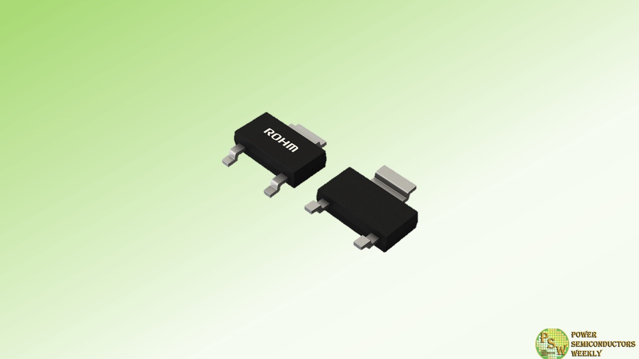
ROHM has added a lineup of compact 600V Super Junction MOSFETs R6004END4 / R6003KND4 / R6006KND4 / R6002JND4 / R6003JND4. These devices are ideal for small lighting power supplies, pumps, and motors.
In recent years, power supplies for lighting and motors for pumps are required to be smaller as devices become more sophisticated – spurring the demand for compact MOSFETs that are essential for switching operation.
Generally, however, it has been difficult to reduce the size of Super Junction MOSFETs while maintaining an optimal balance between high breakdown voltage and low ON resistance. In response, after reviewing the shape of the mounted chip, ROHM was able to develop 5 models in the SOT-223-3 package (6.50mm × 7.00mm × 1.66mm) – providing a smaller, lower profile form factor without compromising the performance of conventional products.
Compared to the conventional TO-252 package (6.60mm × 10.00mm × 2.30mm), ROHM’s new products reduce area and thickness by 31% and 27% – contributing to smaller, lower profile applications. At the same time, the same land pattern (footprint) as the TO-252 package can be used, enabling mounting on existing circuit boards without modification.
Offering distinctive features, three of the models optimized for compact power supplies. The R6004END4, characterized by low noise, is suitable for applications where noise is a concern, while the R6003KND4 and R6006KND4, capable of high-speed switching, are ideal for sets requiring low loss, high efficiency operation.
The R6002JND4 and R6003JND4 utilize proprietary PrestoMOS technology to achieve significantly lower switching losses by speeding up reverse recovery time (trr), making them well-suited for motors-equipped devices.
Supporting materials such as application notes, technical documents, and SPICE simulation models for each product are available on ROHM’s website free of charge to enable quick market introduction.
Going forward, ROHM will continue to expand its Super Junction MOSFET lineup in different packages and even lower ON resistances that contribute to solving social issues such as environmental protection by reducing power consumption in variety devices.
Product Lineup
For compact power supplies
Part No. Data
SheetPolarity
[ch]VDSS
[V]ID
[A]RDS(on) [Ω]
*VGS=10VQg [nC]
*VGS=10VPackage
[mm]Typ. Max. Typ. R6004END4 N 600 2.4 0.90 0.98 15 
SOT-223-3
(6.50×7.00×1.66)R6003KND4 1.3 1.30 1.50 8 R6006KND4 2.8 0.72 0.87 12 For motors
Part No. Data
SheetPolarity
[ch]VDSS
[V]ID
[A]RDS(on) [Ω]
*VGS=15VQg [nC]
*VGS=15Vtrr
[ns]Package
[mm]Typ. Max. Typ. Typ. R6002JND4 N 600 1.0 2.50 3.25 7 40
SOT-223-3
(6.50×7.00×1.66)R6003JND4 1.3 1.65 2.15 8 42 Application Examples
• R6004END4 / R6003KND4 / R6006KND4: Lighting, Air conditioners, Refrigerators, etc.
• R6002JND4 / R6003JND4: Motors for pumps, fans, copiers, etc.Original – ROHM
-
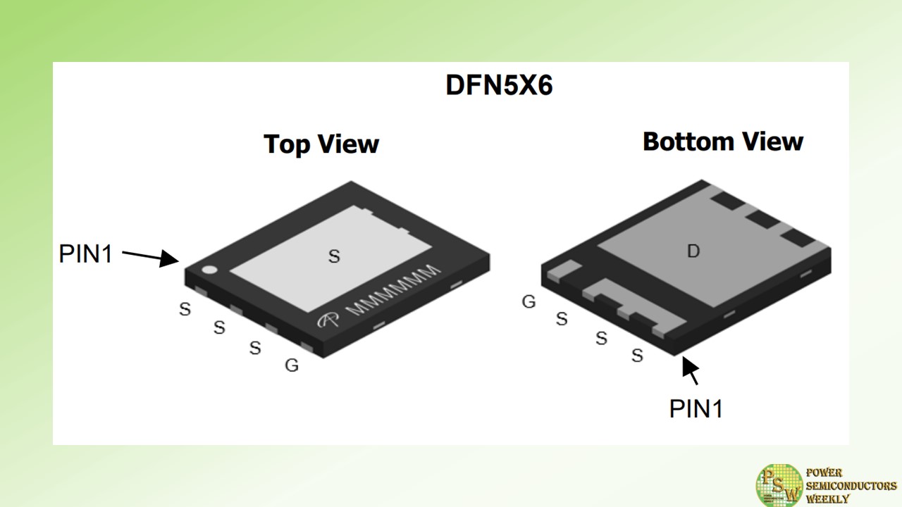
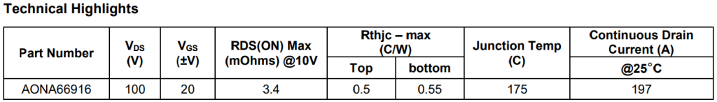
Alpha and Omega Semiconductor Limited (AOS) announced the AONA66916, a 100V MOSFET packaged in the company’s innovatively designed top and bottom side cooling DFN 5 x 6 package. Designers have long trusted AOS power semiconductors as essential components that help them meet a wide variety of high performance application requirements.
Now, in delivering a state-of-the-art package that keeps its semiconductor products cooler, AOS is taking a huge step in enabling engineers to develop more efficient designs in telecommunications and industrial applications that must frequently operate in harsh conditions.
Typically, when using the standard DFN 5×6 package, the bottom contact is the main contributor for cooling, and most of the heat generated by the Power MOSFETs will be transferred to the PCB. This increases the PCB thermal management design considerations to meet system requirements. AOS’ new top and bottom cooling DFN 5×6 package is designed to achieve the highest heat transfer between the exposed top contact and heat sink due to its large surface contact area construction.
This allows the device to achieve a low thermal resistance (Rthc-top max) of 0.5°C / W with results being transferred to the PCB board, enabling significant thermal performance improvements. The top exposed DFN 5×6 package of the AONA66916 shares the same 5mm x 6mm footprint as AOS’ standard DFN 5×6 package, eliminating the need to modify existing PCB layouts.
Another benefit of the AONA66916 is that it utilizes AOS’ 100V AlphaSGT™ technology, providing excellent FOM for balanced performance in hard switching applications. AONA66916 has a maximum RDS(on) rating of 3.4mOhms and has a 175°C junction temperature rating.
“Cooling the power MOSFET in high power design can be challenging, and AOS has successfully addressed this essential issue with our advanced top exposed package design. It not only enables better thermal transfer from its top side exposed contact to heat sink due to large exposed surface area, our new package delivers a much cooler device that contributes to a more efficient and robust final design,” said Peter H. Wilson, Marketing Sr. Director of the MOSFET product line at AOS.
Original – Alpha and Omega Semiconductor
