
-

Qorvo® unveiled an automotive-qualified silicon carbide (SiC) field effect transistor (FET) offering an industry-best 9mΩ RDS(on) in a compact D2PAK-7L package. This 750V SiC FET is the first in a new family of pin-compatible SiC FETs from Qorvo with RDS(on) options up to 60mΩ, making them well suited for electric vehicle (EV) applications, including on-board chargers, DC/DC converters and positive temperature coefficient (PTC) heater modules.
The UJ4SC075009B7S features a 9mΩ typical RDS(on) at 25°C needed for reducing conduction losses and maximizing efficiency in high voltage, multi-kilowatt automotive applications. Its small, surface-mount package enables automated assembly flows and reduces customer manufacturing costs. This new 750V family complements Qorvo’s existing 1200V and 1700V automotive SiC FETs in D2PAK packaging to form a complete portfolio addressing EV applications that span 400V and 800V battery architectures.
Ramanan Natarajan, director of Product Line Marketing for Qorvo’s Power Products, said, “The launch of this new family of SiC FETs demonstrates our commitment to providing EV powertrain designers the most advanced and efficient solutions for their unique automotive power challenges.”
These fourth generation SiC FETs leverage Qorvo’s unique cascode circuit configuration, in which a SiC JFET is co-packaged with a Si MOSFET to produce a device with the efficiency advantages of wide bandgap switch technology and the simpler gate drive of silicon MOSFETs. Efficiency in SiC FETs is dependent on conduction losses, and Qorvo’s cascode/JFET approach enables reduced conduction losses through industry-best RDS(on) and body diode reverse voltage drop.
The key features of the UJ4SC075009B7S include:
- Threshold voltage VG(th): 4.5V (typical) allowing 0 to 15V drive
- Low body diode VFSD: 1.1V
- Maximum operating temperature: 175°C
- Excellent reverse recovery: Qrr = 338 nC
- Low gate charge: QG = 75 nC
- Automotive Electronics Council (AEC) Q101-qualified
Original – Qorvo
-
Mitsubishi Electric Corporation announced the coming release of six new J3-Series power semiconductor modules for various electric vehicles (xEVs), featuring either a silicon carbide metal-oxide semiconductor field-effect transistor (SiC-MOSFET) or a RC-IGBT (Si), with compact designs and scalability for use in the inverters of electric vehicles (EVs) and plug-in hybrid electric vehicles (PHEVs). All six J3-Series products will be available for sample shipments from March 25.
The new power modules will be exhibited at the 38th Electronics R&D, Manufacturing and Packaging Technology Expo (NEPCON JAPAN 2024) from January 24 to 26 at Tokyo Big Sight, Japan, as well as other exhibitions in North America, Europe, China and additional locations.
As power semiconductors capable of efficiently converting electricity expand and diversify in response to decarbonization initiatives, the demand is increasing for SiC power semiconductors offering significantly reduced power loss. In the xEV sector, power semiconductor modules are used widely in power conversion devices such as inverters for xEV drive motors.
In addition to extending the cruising range of xEVs, compact, high-power, high-efficiency modules are needed to further downsize batteries and inverters. But due to the high safety standards set for xEVs, power semiconductors used in drive motors must be more reliable than those used in general industrial applications.
Development of these SiC products was partially supported by Japan’s New Energy and Industrial Technology Development Organization (NEDO).
Original – Mitsubishi Electric
-

Infineon Technologies AG and Wolfspeed, Inc. announced the expansion and extension of their existing long-term 150mm silicon carbide wafer supply agreement, originally signed in February 2018. The extended partnership includes a multi-year capacity reservation agreement.
It contributes to Infineon’s general supply chain stability, also with regard to the growing demand for silicon carbide semiconductor products for automotive, solar and EV applications and energy storage systems.
“As the demand for silicon carbide devices continues to increase, we are following a multi-source strategy to secure access to a high-quality, global and long-term supply base of 150mm and 200mm SiC wafers. Our prolonged partnership with Wolfspeed further strengthens Infineon’s supply chain resilience for the coming years,” said Jochen Hanebeck, CEO of Infineon Technologies. “We have been working with Wolfspeed for more than 20 years to bring the promise of silicon carbide to the automotive, industrial and energy markets, and to help customers leverage this energy-efficient technology to foster decarbonization.”
The adoption of silicon carbide-based power solutions is rapidly growing across multiple markets. Silicon carbide solutions enable smaller, lighter and more cost-effective designs, converting energy more efficiently to unlock new clean energy applications. To better support these growing markets, Infineon is continuously diversifying its supplier base to secure access to high-quality silicon carbide substrates.
“Wolfspeed is the world’s leader in silicon carbide production. We are the catalyst in the industry transition to silicon carbide, providing high-quality materials to key customers like Infineon, a leading supplier in both the automotive and industrial markets, while also scaling our capacity footprint,” said Wolfspeed president and CEO Gregg Lowe. “Industry estimates indicate demand for silicon carbide devices, as well as the supporting material, will grow substantially through 2030, representing a $20 billion annual opportunity. We are very pleased to continue our partnership with Infineon and to serve as a major supplier of silicon carbide wafers in the years ahead.”
Original – Infineon Technologies
-
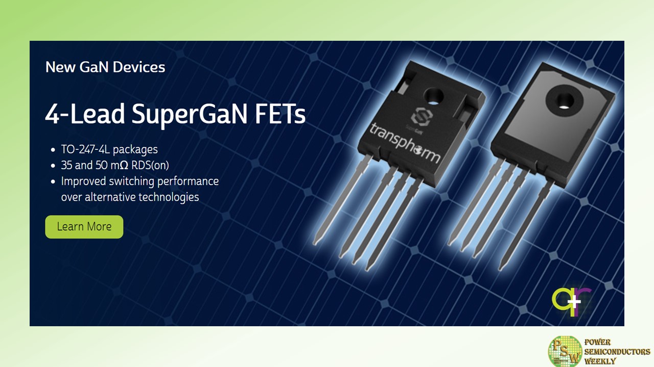
Transphorm, Inc. announced availability of two new SuperGaN® devices in a 4-lead TO-247 package (TO-247-4L). The new TP65H035G4YS and TP65H050G4YS FETs offer a 35 mOhm and 50 mOhm on resistance respectively, complete with a kelvin-source terminal that gives customers versatile switching capabilities with even lower energy losses.
The new products will run on Transphorm’s well-established GaN-on-Silicon substrate manufacturing process that is cost-effective, reliable, and well-suited for high volume manufacturing on silicon production lines. The 50 mOhm TP65H050G4YS FET is currently available while the 35mOhm TP65H035G4YS FET is sampling and slated for release in calendar Q1’2024.
Transphorm’s 4-lead SuperGaN devices can serve as an original design-in option or as a drop-in replacement for 4-lead silicon and SiC solutions supporting power supplies at 1 kilowatt and up in a wide range of data center, renewables, and broad industrial applications. As noted, the 4-lead configuration offers flexibility to users for further improved switching performance.
In a hard-switched synchronous boost converter, the 35 mOhm SuperGaN 4-lead FET reduced losses by 15 percent at 50 kilohertz (kHz) and by 27 percent at 100 kHz when compared to a SiC MOSFET device with a comparable on resistance.
Transphorm’s SuperGaN FETs are known for delivering differentiating advantages such as:
- Industry-leading robustness with a +/- 20 V gate threshold and a 4 V noise immunity.
- Easier designability by reducing the amount of circuitry required around the device.
- Easier drivability as FETs can pair with well-known, off-the shelf drivers common to silicon devices.
The TO-247-4L devices offer the same robustness, designability, and drivability with the following core specifications:
Part Number Vds (V) min Rds(on) (mΩ) typ Vth (V) typ Id (25°C) (A) max Package Variation TP65H035G4YS 650 35 3.6 46.5 Source TP65H050G4YS 650 50 4 35 Source “We continue to expand our product portfolio to bring to market GaN FETs that help customers leverage our SuperGaN platform performance advantages in whatever design requirement they may have,” said Philip Zuk, Senior Vice President, Business Development and Marketing, Transphorm.
“The four-lead TO-247 package provides flexibility for designers and customers seeking even greater power system loss reductions with little to no design modifications on silicon or silicon carbide systems. It’s an important addition to our product line as we ramp into higher power applications.”
Original – Transphorm
-
Renesas Electronics Corporation and Transphorm, Inc. announced that they have entered into a definitive agreement pursuant to which a subsidiary of Renesas will acquire all outstanding shares of Transphorm’s common stock for $5.10 per share in cash, representing a premium of approximately 35% to Transphorm’s closing price on January 10, 2024, a premium of approximately 56% to the volume weighted average price over the last twelve months and a premium of approximately 78% to the volume weighted average price over the last six months.
The transaction values Transphorm at approximately $339 million. The acquisition will provide Renesas with in-house GaN technology, a key next-generation material for power semiconductors, expanding its reach into fast-growing markets such as EVs, computing (data centers, AI, infrastructure), renewable energy, industrial power conversion and fast chargers/adapters.
Demand for highly efficient power systems is increasing as building blocks for carbon neutrality. To address this trend, an industry-wide transition toward wide bandgap (“WBG”) materials, represented by silicon carbide (“SiC”) and GaN, is also being seen. These advanced materials allow a broader range of voltage and switching frequency than conventional silicon-based devices. To build on this momentum, Renesas has announced the establishment of an in-house SiC production line, supported by a 10 year SiC wafer supply agreement.
Renesas now aims to further expand its WBG portfolio with Transphorm’s expertise in GaN, an emerging material that enables higher switching frequency, lower power losses, and smaller form factors. These benefits empower customers’ systems with greater efficiency, smaller and lighter composition, and lower overall cost.
As such, demand for GaN is predicted to grow by more than 50 percent annually, according to an industry study. Renesas will implement Transphorm’s auto-qualified GaN technology to develop new enhanced power solution offerings, such as X-in-1 powertrain solutions for EVs, along with computing, energy, industrial and consumer applications.
“Transphorm is a company uniquely led by a seasoned team rooted in GaN power and with origins from the University of California at Santa Barbara,” said Hidetoshi Shibata, CEO of Renesas. “The addition of Transphorm’s GaN technology builds on our momentum in IGBT and SiC. It will fuel and expand our power portfolio as a key pillar of growth, offering our customers the full ability to choose their optimal power solutions.”
“Combined with Renesas’ world-wide footprint, breadth of solution offerings and customer relationships, we are excited to pave the way for industry-wide adoption of WBG materials and set the stage for significant growth.
This transaction will also allow us to offer further expanded services to our customers and deliver significant immediate cash value to our stockholders,” said Dr. Primit Parikh, Co-founder, President and CEO of Transphorm and Dr. Umesh Mishra, Co-founder and CTO of Transphorm. “Additionally, it will provide a strong platform for our exceptional team to further Transphorm’s leading GaN technology and products.”
The board of directors of Transphorm has unanimously approved the definitive agreement with respect to the transaction and recommended that Transphorm stockholders adopt such definitive agreement and approve the merger. Concurrently with the execution of the definitive agreement, KKR Phorm Investors L.P., which holds approximately 38.6% of Transphorm’s outstanding common stock, has entered into a customary voting agreement with Renesas to vote in favor of the transaction.
The transaction is expected to close in the second half of calendar year 2024, subject to Transphorm stockholder approval, required regulatory clearances and the satisfaction of other customary closing conditions.
Original – Renesas Electronics
-

Infineon Technologies AG has formalized an agreement with silicon carbide (SiC) supplier SK Siltron CSS. Under the agreement, SK Siltron CSS will provide Infineon with competitive and high-quality 150-millimeter SiC wafers, supporting the production of SiC semiconductors. In a subsequent phase, SK Siltron CSS will play an important role in assisting Infineon’s transition to a 200-millimeter wafer diameter.
“For Infineon, supply chain resiliency is about implementing a multi-supplier strategy and thriving in times of adversity to create new growth opportunities and drive decarbonization,” said Angelique van der Burg, Chief Procurement Officer at Infineon. “We are excited to partner with SK Siltron CSS to serve the growing SiC demand of our broad customer base with new energy-efficient and top-quality products, matching the highest standards in the SiC market.”
“With decades of experience in silicon carbide materials and manufacturing, we bring unparalleled knowledge to our sustainably manufactured compound semiconductor solutions. This wealth of experience is a cornerstone in our partnership with Infineon,” said Jianwei Dong, Ph.D., CEO of SK Siltron CSS. “This long-term supply agreement marks the synergy of our extensive expertise and Infineon’s vision to make life easier, safer and greener for generations to come.”
Original – Infineon Technologies
-
STMicroelectronics announced its new organization, effective February 5th, 2024.
“We are re-organizing our Product Groups to further accelerate our time-to-market and speed of product development innovation and efficiency. This will enable us to increase value extraction from our broad and unique product and technology portfolio. In addition, we are getting even closer to our customers with an application marketing organization by end market which will boost our ability to complement our product offering with complete system solutions” said Jean-Marc Chery, President and CEO of STMicroelectronics. “This is an important step in the development of our established strategy, in line with our value proposition to all stakeholders and with the business and financial ambitions we set back in 2022”.
Moving from three to two Product Groups to further enhance product development innovation and efficiency, and time-to-market
The two new Product Groups will be:
- Analog, Power & Discrete, MEMS and Sensors (APMS), led by Marco Cassis, ST President and member of the Executive Committee; and
- Microcontrollers, Digital ICs and RF products (MDRF), led by Remi El-Ouazzane, ST President and member of the Executive Committee.
The APMS Product Group will include all ST analog products, including Smart Power solutions for automotive; all ST Power & Discrete product lines including Silicon Carbide products; MEMS and Sensors.
APMS will include two Reportable Segments: Analog products, MEMS and Sensors (AM&S); Power and discrete products (P&D).The MDRF Product Group will include all ST digital ICs and microcontrollers, including automotive microcontrollers; RF, ADAS, Infotainment ICs. MDRF will include two Reportable Segments: Microcontrollers (MCU); Digital ICs and RF Products (D&RF).
Concurrent with this new organization Marco Monti, ST President of the former Automotive and Discrete Product Group, will leave the Company.
To complement the existing Sales & Marketing organization, a new application marketing organization by end market will be implemented across all ST Regions. This will provide ST customers with end-to-end system solutions based on the Company’s product and technology portfolio.
The company is implementing an application marketing organization by end market across all ST Regions, as part of its Sales & Marketing organization led by Jerome Roux, ST President and member of the Executive Committee. The application marketing organization will cover the following four end markets:
- Automotive
- Industrial Power and Energy
- Industrial Automation, IoT and AI
- Personal Electronics, Communication Equipment and Computer Peripherals.
The current regional Sales & Marketing organization remains unchanged.
Original – STMicroelectronics
-
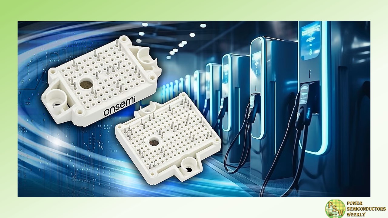
onsemi announced the availability of nine new EliteSiC Power Integrated Modules (PIMs) enabling bidirectional charging capabilities for DC ultra-fast electric vehicle (EV) chargers and energy storage systems (ESS). The silicon carbide-based solutions will dramatically improve system cost with higher efficiency and simpler cooling mechanisms that can reduce size by up to 40% and weight by up to 52% compared to traditional silicon-based IGBT solutions.
With more compact, lighter charging platforms, designers will have all the key building blocks that are needed to quickly deploy a reliable, efficient and scalable network of DC fast chargers that can charge electric vehicle batteries up to 80% in as little as 15 minutes.
According to J.D. Power’s 2023 Electric Vehicle Consideration Study, nearly half of U.S. consumers note the reason for not purchasing an electric vehicle is the access to charging and the ability to do so quickly, to ensure the driving experience is as easy and seamless as with a traditional internal combustion engine (ICE) vehicle. In the U.S., the availability of EV chargers needs to quadruple by 2025 and 8x by the end of the decade to keep up with demand and ensure drivers have equitable access to public charging stations.
In turn, this rapid increase in demand for electricity will also put a tremendous strain on current electrical grids, potentially overloading them. To mitigate this problem, bidirectional charging has emerged as a key solution to implement vehicle-to-grid which allows both regular battery charging and the ability to use an EV as an energy storage system to power your home when needed.
This solution helps enable a DC fast charging network and vehicle-to-grid power transfer systems, addressing access and speed with its ability to recharge a vehicle faster than other methods that take hours or even days.
onsemi offers the most comprehensive portfolio of PIMs to address the key topologies on the market. This gives designers the flexibility to pick the right PIM for power conversion stages in their DC fast charging or energy storage system applications. To accelerate the design cycle, advanced piecewise linear electrical circuit simulation (PLECS) models through our Self-Service PLECS model Generator and application simulation with the Elite Power Simulator of this portfolio will also be made available to designers.
For each module, onsemi uses die from the same wafer to ensure more consistency and reliability so designers don’t have to use discretes from different suppliers, which can lead to varying performance results. In addition to its reliability, this module portfolio offers the following benefits:
- Uses the Gen3 M3S SiC MOSFET technology which offers the lowest switching losses and highest efficiency in the industry
- Supports key topologies such as multi-level T-type neutral point clamp (TNPC), half-bridge and full-bridge topologies
- Supports scalable output power from 25 kW to 100 kW, enabling multiple DC fast charging and energy storage systems platforms including bidirectional charging
- Industry-standard F1 and F2 packages with the option of pre-applied Thermal Interface Material (TIM) and press fit pins
- Enables optimal thermal management, avoiding system failure due to overheating
- Full SiC modules offer energy conservation by minimizing power losses, directly translating to cost and energy savings
- Offers more robustness and dependability, ensuring consistent operations
Original – onsemi
-
STMicroelectronics has signed a long-term silicon carbide (SiC) supply agreement with Li Auto, a leader in China’s new energy vehicle market that designs, develops, manufactures, and sells smart premium electric vehicles. Under this agreement, STMicroelectronics will provide Li Auto with SiC MOSFET devices to support Li Auto’s strategy around high-voltage battery electric vehicles (BEVs) in various market segments.
As the automotive industry transforms towards electrification and decarbonization, high-voltage BEVs have become a popular choice for car makers. These vehicles offer outstanding energy efficiency and extended mileage. Li Auto, known for its extended-range electric vehicles (EREVs), is entering the BEV market with its first-ever high-tech flagship family MPV BEV model premiered in Q4 2023. With plans to introduce more high-voltage BEV models soon, Li Auto will require high volumes of SiC MOSFETs that it will integrate into its traction inverters to ensure superior electric-vehicle performance.
ST’s SiC devices increase performance and efficiency through higher switching frequencies, breakdown voltages, and thermal resistance. These are all particularly critical characteristics at the higher operating voltages required for battery electric vehicles. Li Auto is adopting ST’s advanced third-generation 1200V SiC MOSFET in the traction inverter of its upcoming 800V BEV platform, to ensure industry-leading process stability and performance, efficiency, and reliability.
“Li Auto is committed to providing families with premium EVs exceeding their expectation. This agreement with ST stands as a testament to Li Auto’s unwavering dedication in BEV product development. Collaborating with the renowned global leader in SiC technologies, we anticipate a forthcoming relationship filled with innovation and success,” said Qingpeng MENG, Vice President of Supply Chain, Li Auto.
Holding more than 50% market share in SiC MOSFETs worldwide, ST’s SiC technology has earned high praise from top OEMs for its electric-vehicle performance. It is widely used in onboard chargers and power modules.
“As a world leader in power devices and wide bandgap semiconductor technologies, ST has established long-term supply agreements with major car makers and Tier 1 suppliers. The SiC supply agreement with Li Auto marks a significant step building upon our existing long-term relationship in other automotive applications,” said Henry CAO, Executive Vice President of Sales & Marketing, China Region, STMicroelectronics. “ST is committed to supporting Li Auto’s ambition to become a top premium electric vehicle brand in China, offering their customers superior vehicle performance and range with our innovative SiC technologies.”
Original – STMicroelectronics
-
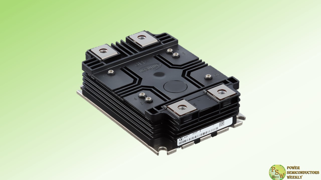
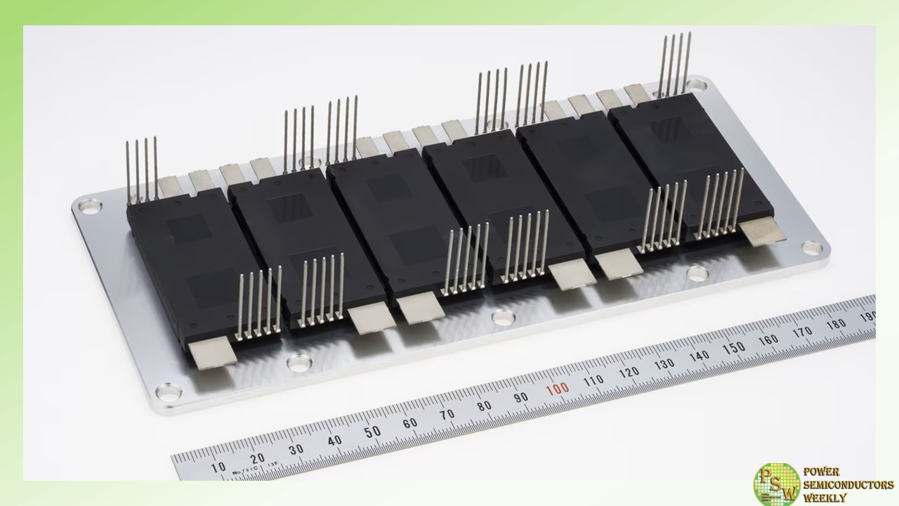
The paradigm shift towards offloading complexity to suppliers and adopting smaller IGBT modules is evident in various applications. In response to the global push for downsizing and integration, Infineon Technologies AG introduced the 4.5 kV XHP™ 3 IGBT modules that will fundamentally change the landscape for medium voltage drives (MVD) and transportation applications operating at 2000 to 3300 V AC in 2- and 3-level topologies.
Applications benefiting from the new devices include large conveyor belts, pumps, high-speed trains, locomotives, as well as commercial, construction and agricultural vehicles (CAV).
The XHP family comprises a 450 A dual IGBT module with TRENCHSTOP™ IGBT4 and an emitter-controlled diode, and a 450 A double diode module with emitter-controlled E4 Diode. Both modules feature improved isolation of 10.4 kV. Together, they help to simplify paralleling and downsizing without sacrificing efficiency.
Previously, complex busbars were required to parallelize switching modules, resulting in complicated design efforts and leakage inductance. The innovative design of the XHP family simplifies paralleling by conveniently placing the connections side by side. As a result, only a single straight busbar is required for paralleling.
The 4.5 kV XHP family also allows developers to reduce the number of units. Conventional IGBT solutions use multiple single switches and a double diode. With the new devices, however, designs can be reduced to two dual switches and a smaller double diode – a significant step forward in integrated drives.
The combination of the XHP 3 FF450R45T3E4_B5 dual switch and the DD450S45T3E4_B5 double diode enables significant cost savings and a smaller footprint. For example, Infineon’s previous IGBT solutions required four 140 x 190 mm² or 140 x 130 mm² switches and one 140 x 130 mm² double diode. With the new XHP family, the components can be reduced to two 140 x 100 mm² dual switches and a smaller 140 x 100 mm² double diode.
The IGBT modules FF450R45T3E4_B5 and DD450S45T3E4_B5 are available now. More information is available at www.infineon.com/XHP.
Original – Infineon Technologies