-
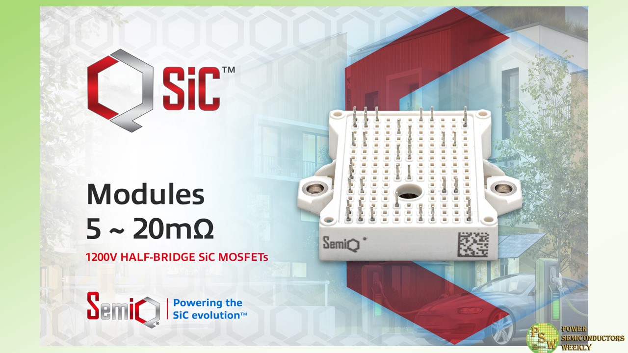
SemiQ Inc has expanded its QSiC™ power modules portfolio with the introduction of a new series of 1200V silicon-carbide (SiC) power MOSFETs in half-bridge packages.
Engineered and tested to operate reliably in demanding environments, these new compact, high-performance modules enable high-power-density implementations while minimizing dynamic and static losses.
Featuring high breakdown voltage (>1400V), the new QSiC™ modules support high-temperature operation (Tj = 175°C) with low Rds(On) shift over the full temperature range. In addition, the modules exhibit industry-leading gate oxide stability and long gate oxide lifetime, avalanche unclamped inductive switching (UIS) ruggedness and long short-circuit withstand time.
With a solid foundation of high-performance ceramics, the new SiC modules are suitable for EV charging, on-board chargers (OBCs), DC-DC converters, E-compressors, fuel cell converters, medical power supplies, photovoltaic inverters, energy storage systems, solar and wind energy systems, data center power supplies, UPS/PFC circuits, Vienna rectifiers, and other automotive and industrial applications.
To ensure that each module has a stable gate threshold voltage and high-quality gate oxide, SemiQ’s modules undergo gate burn-in testing at the wafer level. Besides the burn-in test, which helps to stabilize the extrinsic failure rate, stress tests such as gate stress, high-temperature reverse bias (HTRB) drain stress, and high humidity, high voltage, high temperature (H3TRB) allow achieving the required automotive and industrial grade quality levels. The devices also have extended short-circuit ratings. All modules have undergone testing exceeding 1350V.
Dr. Timothy Han, President at SemiQ, said, “SemiQ’s commitment to reliability and testing sets us apart in the semiconductor industry. Our high-performance QSiC™ 1200V MOSFET modules are proven to withstand challenging conditions, enabling engineers to develop reliable systems for the renewable, automotive, medical, and industrial sectors.”
SemiQ’s new 1200V 5mΩ, 10mΩ, and 20mΩ SiC MOSFET are available in industry standard half-bridge packages.
Part Number Circuit Configuration Ratings Typ. RdsOn [mΩ] GCMX010A120B2B1P Half-bridge 1200V/214A, B2 9 GCMX020A120B2B1P Half-bridge 1200V/102A, B2 19 GCMX005A120B3B1P Half-bridge 1200V/383A, B3 4.4 GCMX010A120B3B1P Half-bridge 1200V/173A, B3 9 Original – SemiQ
-
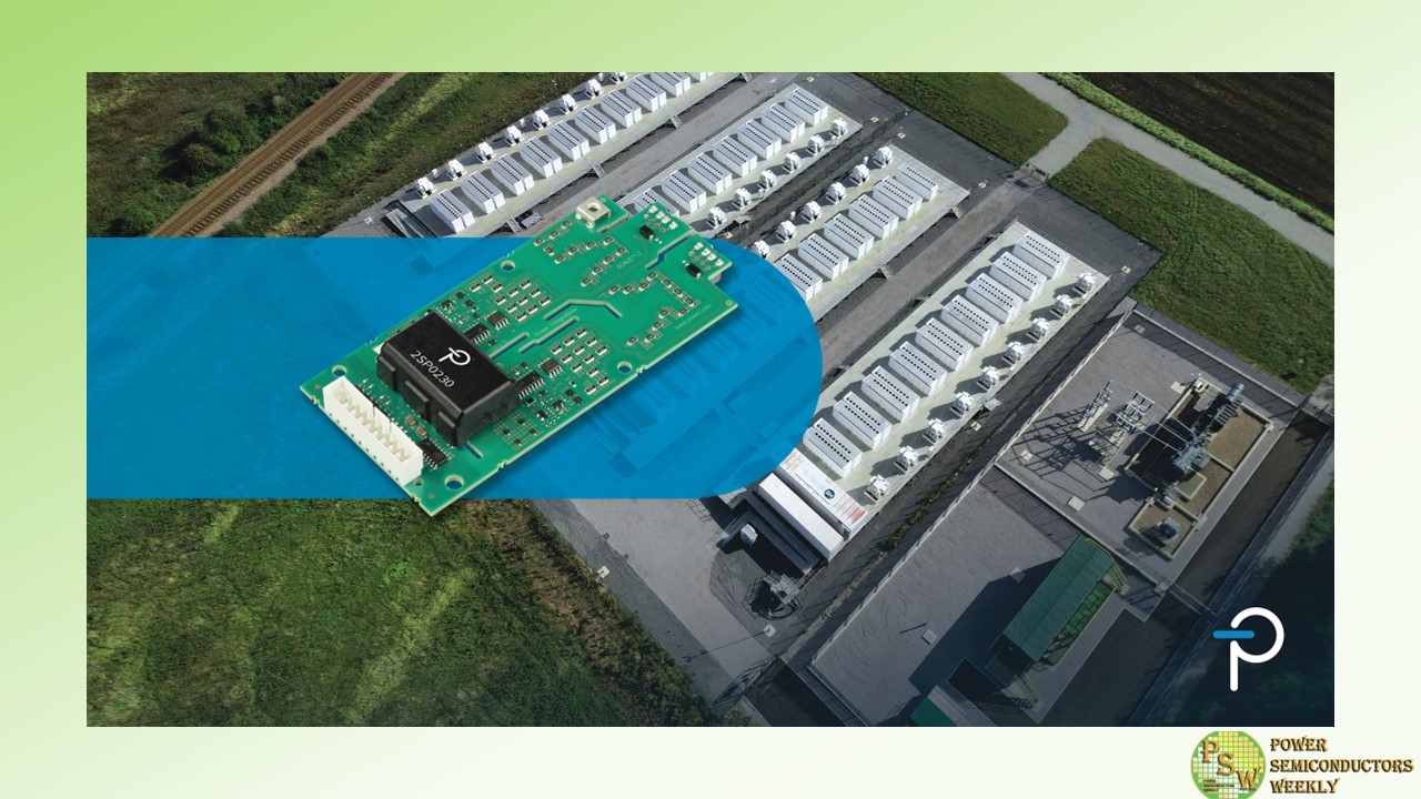
Power Integrations announced a new family of plug-and-play gate drivers for 62 mm silicon-carbide (SiC) MOSFET and silicon IGBT modules rated up to 1700 V, with enhanced protection features to ensure safe, reliable operation.
SCALE™-2 2SP0230T2x0 dual-channel gate drivers deploy short-circuit protection in less than two microseconds, protecting the compact SiC MOSFETs against damaging over-currents. The new drivers also include advanced active clamping (AAC) to protect the switches against over-voltage during turn-off, enabling higher DC link operating voltages.
Thorsten Schmidt, product marketing manager at Power Integrations, commented: “The 2SP0230T2x0 gate drivers are flexible; the same hardware can be used to drive either SiC MOSFET or IGBT modules. This reduces both system design and sourcing challenges, and the plug-and-play approach speeds development.”
Ideal for applications such as railway auxiliary converters, offboard EV chargers and STATic synchronous COMpensator (STATCOM) voltage regulators for the power grid, 2SP0230T2x0 gate drivers are based on Power Integrations’ proven SCALE-2 technology, resulting in higher levels of integration, smaller size, more functionality and enhanced system reliability.
Power Integrations’ compact 134 x 62 mm 2SP0230T2x0 provides reinforced isolation at 1700 V, enabling use for up to 1700 V operation; this is 500 V higher than conventional drivers, which are typically limited to 1200 V.
Original – Power Integrations
-
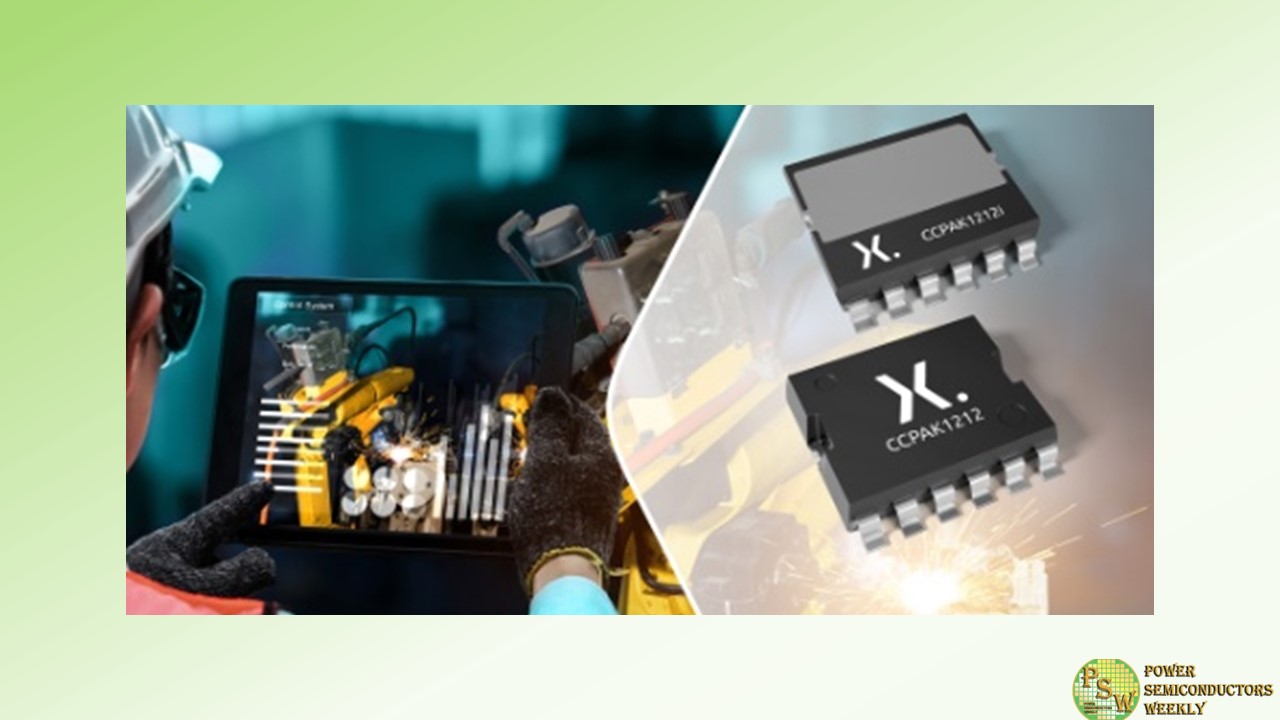
Nexperia announced that its GaN FET devices, featuring next-gen high-voltage GaN HEMT technology in proprietary copper-clip CCPAK surface mount packaging, are now available to designers of industrial and renewable energy applications.
Building on two decades of expertise in supplying high-volume, high-quality copper-clip SMD packaging, Nexperia is now proud to extend its revolutionary packaging approach to GaN cascode switches in CCPAK. The GAN039-650NTB, a 33 mΩ (typ.) Gallium Nitride (GaN) FET within the CCPAK1212i top-side cooling package, ushers in a new era of wide bandgap semiconductors and copper-clip packaging.
This technology offers advantages for renewable energy applications such as solar and residential heat pumps, further enhancing Nexperia’s commitment to developing the latest component technology for sustainable applications. It is also suited to a wide spectrum of industrial applications such as servo drives, switched-mode power supplies (SMPS), server, and telecom.
Nexperia’s CCPAK surface mount packaging uses Nexperia’s proven innovative copper-clip package technology to replace internal bond wires. This reduces parasitic losses, optimizes electrical and thermal performance, and improves device reliability. For maximum flexibility in designs, these CCPAK GaN FETs are available in top- or bottom-cooled configurations to further improve heat dissipation.
The cascode configuration of the GAN039-650NTB enables it to deliver superior switching and on-state performance, with a robust gate offering high margins against noise. This feature also simplifies application designs by eliminating the requirement for complex gate drivers and control circuitry, instead allowing them to be conveniently driven using standard silicon MOSFET drivers.
Nexperia’s GaN technology improves switching stability and helps to shrink die size by approximately 24%. In addition, device RDS(on) is reduced to only 33 mΩ (typ.) at 25°C, with a high threshold voltage and low diode forward voltage.
“Nexperia recognizes that designers of industrial and renewable energy equipment need a highly robust switching solution that can provide excellent thermal efficiency when performing power conversion.”, according to Carlos Castro, Vice President and General Manager of the GaN FET business at Nexperia. “This is why Nexperia decided to bring together the exceptional switching performance of its cascode GaN FETs with the exceptional thermal properties of its CCPAK packaging to offer customers a compelling solution.”
Nexperia begins its CCPAK portfolio release with the top-cooled 33 mΩ (typ.), 650 V GAN039-650NTB, and will follow shortly with the bottom-cooled variant, GAN039-650NBB of the same RDS(on). More information including datasheets and samples is available at www.nexperia.com/ccpak.
Original – Nexperia
-
A plan by ROHM Co., Ltd. and Toshiba Electronic Devices & Storage Corporation to collaborate in the manufacture and increased volume production of power devices has been recognized and will be supported by the Ministry of Economy, Trade and Industry as a measure supporting the Japanese Government’s target of secure and stable semiconductor supply.
ROHM and Toshiba Electronic Devices & Storage will respectively make intensive investments in silicon carbide (SiC) and silicon (Si) power devices, effectively enhance their supply capabilities, and complementally utilize other party’s production capacity.
Power devices are essential components for supplying and managing power supply in all kinds of electronic equipment, and for achieving a carbon-free, carbon-neutral society. Current demand is expected to see continued growth.
In automotive applications, development of more efficient, smaller and lighter electric powertrains has advanced alongside the rapid expansion in vehicle electrification. In industrial applications, stable supply of power devices and improved characteristics are widely required to support increasing automation and higher efficiency requirements.
Against this backdrop, ROHM has formulated a management vision, “We focus on power and analog solutions and solve social problems by contributing to our customers’ needs for energy savings and miniaturization of their products.,” and accelerates its efforts for a carbon-free. SiC power devices are the keys to energy savings.
Since the world’s first mass production of SiC MOSFETs, ROHM has been constantly developing industry-leading technologies. Among these are ROHM’s latest 4th Generation SiC MOSFETs that will be adopted for numerous electric vehicles and industrial equipment. As one of its priority projects, ROHM is working on SiC business, which contains aggressive and continuous investment to increase the production capacity of SiC and meet strong demand growth.
Toshiba Group, with its long-standing Basic Commitment, “Committed to People, Committed to the Future.,” aims to advance the achievement of carbon neutrality and a circular economy. Toshiba Electronic Devices & Storage has for decades supplied Si power devices, mainly for automotive and industrial markets, that have helped to secure energy saving solutions and equipment miniaturization.
The company started production on a 300mm wafer line last year, and is accelerating investment to enhance production capacity and meet strong demand growth. It is also advancing development of a wider lineup of SiC power devices, especially for automotive and power transmission and distribution applications, taking full advantage of the expertise it has cultivated in railway vehicle applications.
ROHM has already announced its participation in the privatization of Toshiba, but this investment did not serve as the starting point for manufacturing collaboration between the two companies. Under intensifying international competition in the semiconductor industry, ROHM and Toshiba Electronic Devices & Storage have been considering collaboration in the power device business for some time, and that resulted in the joint application.
ROHM and Toshiba Electronic Devices & Storage will collaborate in manufacturing power devices, through intensive investments in SiC and Si power devices, respectively, toward enhancing both companies’ international competitiveness. The companies will also seek to contribute to strengthening the resilience of semiconductor supply chains in Japan.
Original – Toshiba
-
Today some applications tend to increase bus voltage, and using 1200V SiC power modules can no longer correspond to voltage requirements. Using 1700V SiC devices can solve the problem, but it comes with a price.
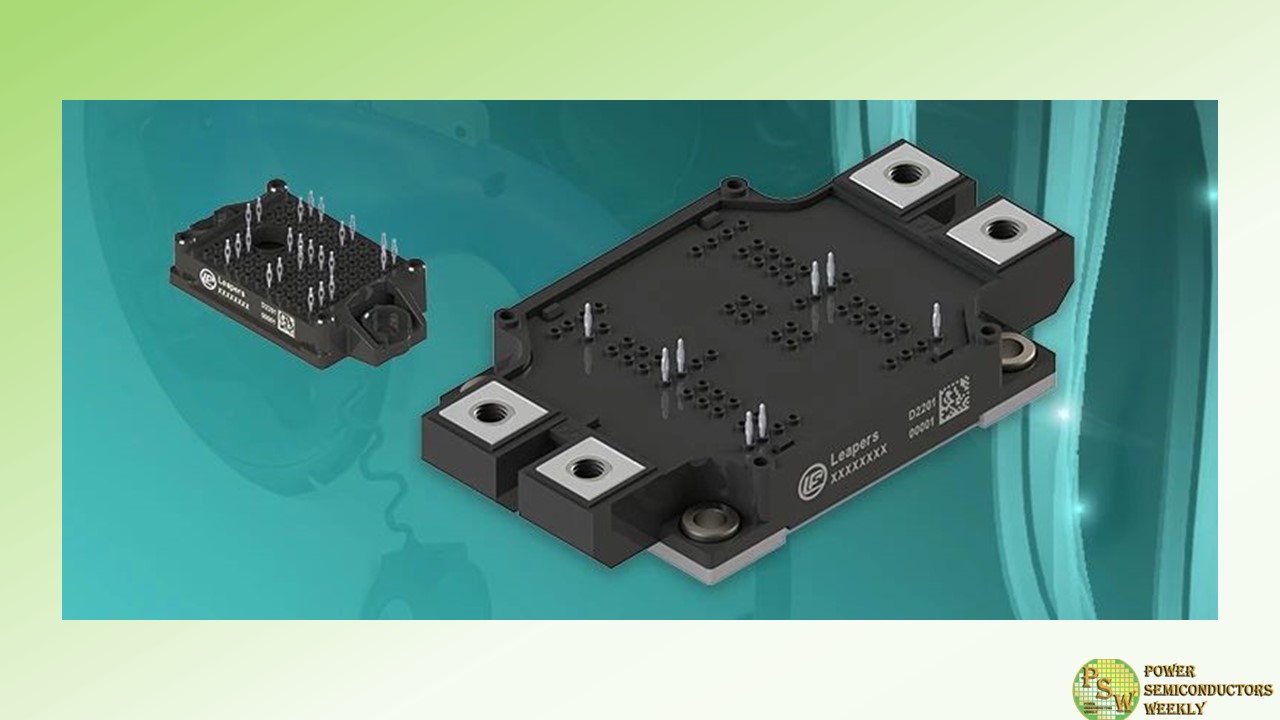
Leapers Semiconductor announced a new series of 1400V SiC power modules in already familiar E0 and ED3S packages. They are the perfect solution to the mentioned problem, providing great performance at affordable price.
At the moment the new series 1400V SiC modules come in Half-Bridge, H-Bridge, and Boost topologies.
Leapers Semiconductor new SiC product family features:
– 1,4kV voltage
– 50 – 600A current
– 3,2 – 40 mOhm Rds(on)
– Epoxy resin
– Si3N4 AMB substrate
– Low thermal resistance
– Low switching lossesFirst batches of 1400V SiC power modules successfully passed field tests by the end customers and soon will be mass used in:
– DC fast chargers
– Commercial EVs
– Power supplies for production of hydrogen
– DC/DC convertersOriginal – Leapers Semiconductor
-
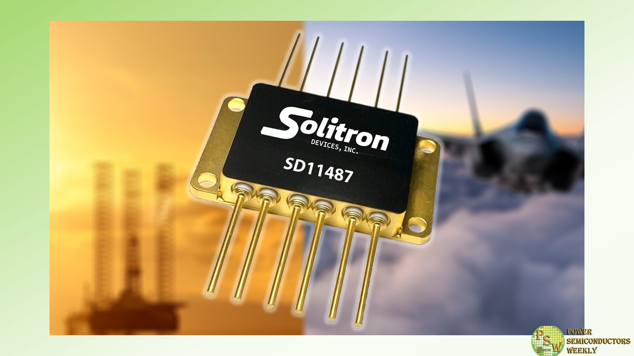
Solitron Devices announced the introduction of the SD11487, the industry’s first hermetically sealed Silicon Carbide (SiC) Power Module for high reliability applications.
With a unique hermetic packaging format, the 51mm x 30mm x 8mm outline is the smallest hermetically sealed high reliability, high voltage, half-bridge on the market. The integrated format maximizes power density while minimizing loop inductance. 60 mil pins for the power output stage are isolated on one side of the package to allow simple power bussing while 30 mil pins are on the opposite side for control signals.
The SD11487 is a half bridge configuration with two 1200V 12mΩ SiC MOSFETs. Also included in the module are two freewheeling 1200V SiC Schottky diodes in parallel with the MOSFETs and an integrated NTC temperature sensor. Continuous drain current is specified at 95A.
With operating temperatures of -55°C to 175°C, the SD11487 is designed for the most demanding applications such as down hole exploration; space; and avionics. The hermetically sealed copper package combined with the Alumina Nitride direct bond copper substrate provide excellent thermal conductivity as well as case isolation. The integrated temperature sensing enables high level temperature protection.
Silicon Carbide provides excellent switching performance versus the best-in-class silicon MOSFETs and IGBTs with minimal variation versus temperature. Higher efficiency levels than silicon due to significantly lower energy loss and reverse charge results in more switching power and less energy required in the switch-on and switch-off phase. Combined with high switching frequencies this translates to smaller magnetics significantly reducing system weight and size.
Original – Solitron Devices
-
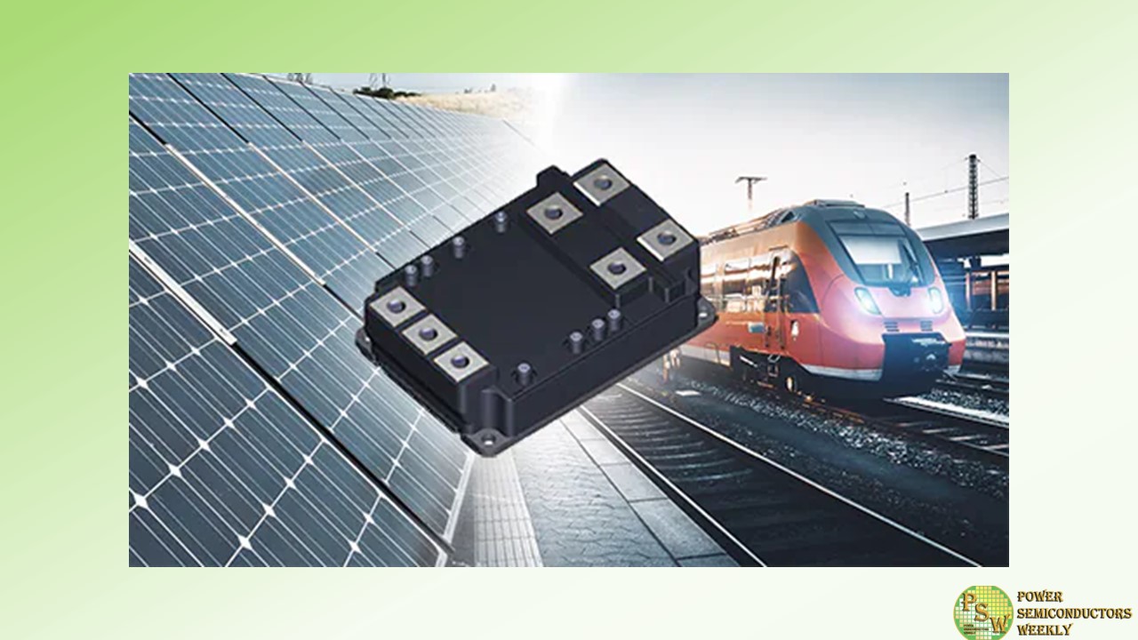
Toshiba Electronic Devices & Storage Corporation has launched chopper SiC MOSFET modules “MG800FXF1ZMS3” and ”MG800FZF1JMS3” with ratings of 3300 V and 800 A using 3rd generation silicon carbide (SiC) MOSFET and SBD chips for industrial equipment and has expanded its lineup.
The new products MG800FXF1ZMS3 and MG800FXF1JMS3 adopt an iXPLV package with Ag sintering internal bonding technology and high compatibility with mounting. These offers low conduction loss with low drain-source on-voltage (sense) of 1.3 V (typ.), and also offers low switching loss with low turn-on switching loss of 230 mJ (typ.) and low turn-off switching loss of 230 mJ (typ.). These contribute to reducing the power loss of equipment and the size of cooling device.
The lineup of Toshiba’s MOSFET modules of iXPLV package has three products, including existing product MG800FXF2YMS3 (3300 V / 800 A / Dual SiC MOSFET module.) This provides a wide range of product selection. This can be used in 2-level inverters, buck/boost converters and 3-level inverters.
Toshiba will continue to meet the market needs for high efficiency and the downsizing of industrial equipment.
Applications
Industrial equipment
- Inverters and converters for railway vehicles
- Renewable energy power generation systems
- Motor control equipment for industrial equipment, etc.
Features
- Low drain-source on-voltage (sense):
VDS(on)sense=1.3 V (typ.) (ID=800 A, VGS=+20 V, Tch=25 °C) - Low turn-on switching loss:
Eon=230 mJ (typ.) (VDD=1800 V, ID=800 A, Tch=175 °C) - Low turn-off switching loss:
Eoff=230 mJ (typ.) (VDD=1800 V, ID=800 A, Tch=175 °C)
Original – Toshiba
-
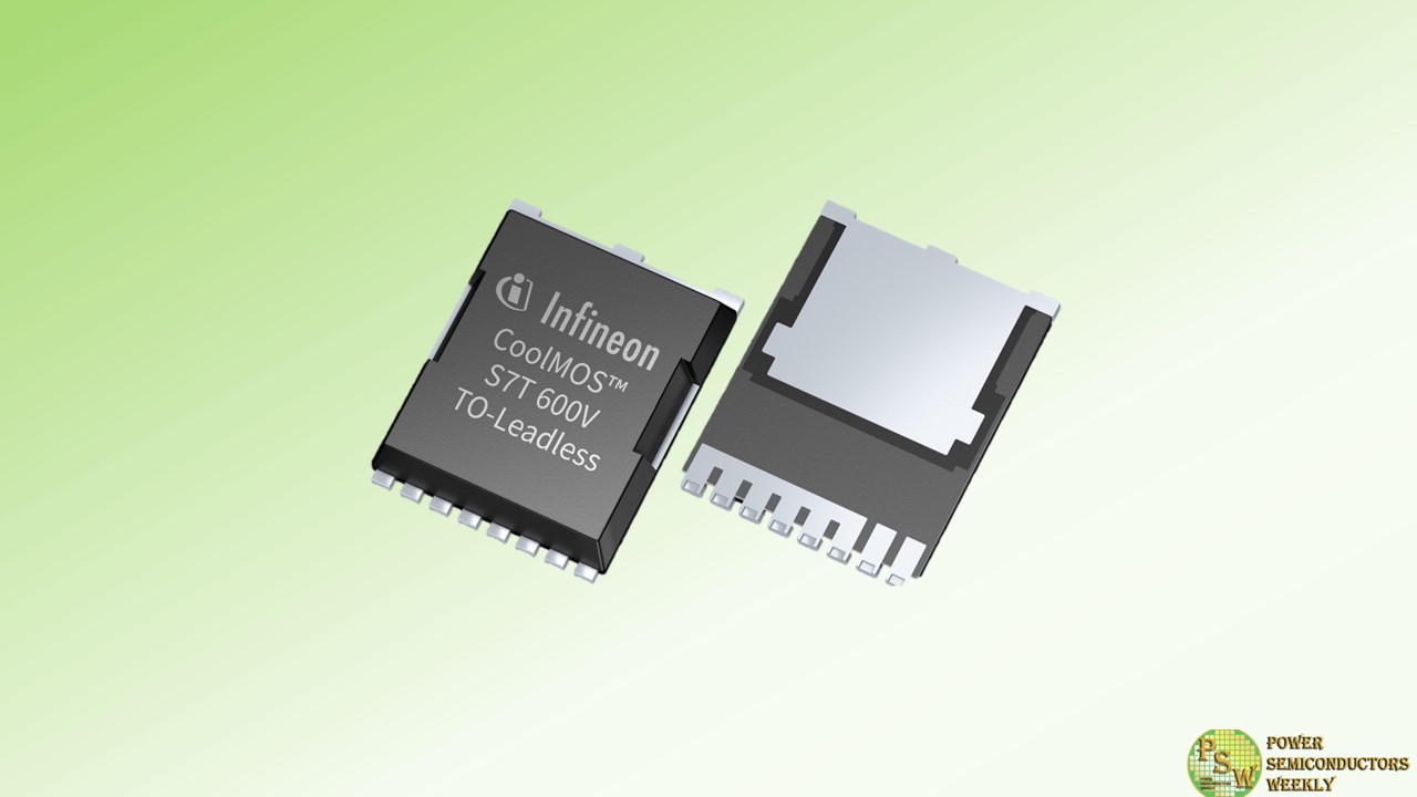
Infineon Technologies AG launches its new CoolMOS™ S7T product family with an integrated temperature sensor to improve the accuracy of junction temperature sensing. The integration of these products has a positive impact on the durability, safety, and efficiency of many electronic applications. The CoolMOS S7T is best suited for solid-state relay (SSR) applications for enhanced performance and reliability due to its superior R DS(on) and the highly accurate, embedded sensor.
Since SSRs are fundamental components in various electronic devices, customers can benefit in many ways from a superjunction MOSFET with an integrated sensor in the same package. Infineon’s innovative approach improves the relay’s performance and ensures reliable operation even under overload conditions. The integrated temperature sensor provides up to 40 percent greater accuracy and ten times faster response time than a standard independent on-board sensor located at the drain. Additionally, the monitoring process can be performed individually within a multi-device system for improved reliability.
The CoolMOS S7T enables optimal utilization of the power transistor, resulting in enhanced performance and precise control of the output stage. Compared to electromechanical relays, the total power dissipation can be improved up to two times, while current solid state triac solutions are more than 5 times less efficient. Improved efficiency and the ability to handle higher loads help in reducing power consumption and energy costs.
Unique output stage performance, coupled with a significant overcurrent threshold, bolster relay reliability and minimizes the risk of failure and downtime. The rugged switching solution also ensures safer operation. As a result of the MOSFETs increased robustness, the life of the relay is improved, leading to less frequent replacement. Ultimately, all of these benefits translate into lower maintenance costs.
Original – Infineon Technologies
-
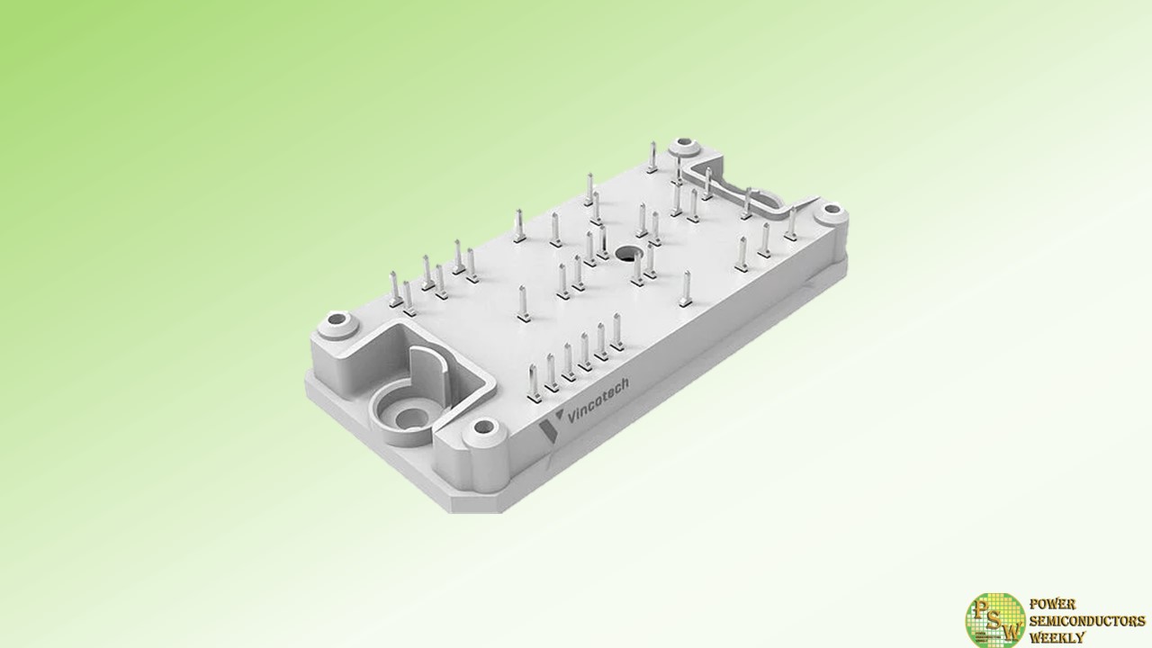
Efficiency is a big deal for heat pumps and HVAC systems that require higher power from a smaller footprint. The new Vincotech power module 1200V PIM+PFC resolves that contradiction by taking efficiency to a whole other level. Featuring a 3-phase ANPFC and an inverter stage, it enables your engineers to design more deeply integrated systems that drive costs down.
Main Benefits
- All-in-one solution: 3-phase PFC with inverter stage in a compact flow1 housing allows for more compact designs and higher power density
- AN-PFC with SiC MOSFETs and SiC diodes for up to 200 kHz: remarkably efficient topology brings down system costs
- Thin Al2O3 substrate facilitates overall thermal design
- Inverter stage featuring SiC MOSFETs for high-frequency switching
- Integrated thermal sensor simplifies temperature measurement
Applications
- Embedded Drives
- HVAC, Heatpumps
Original – Vincotech
-

Coherent Corp. announced that it has closed the $1 billion aggregate investment by DENSO CORPORATION and Mitsubishi Electric Corporation in Coherent’s silicon carbide semiconductor business.
Under the terms of the transaction announced on October 10, 2023, DENSO and Mitsubishi Electric each invested $500 million in exchange for a 12.5% non-controlling ownership interest in the Business, with Coherent owning the remaining 75%. Coherent has separated and contributed the Business to a new subsidiary that will operate the Business. Going forward, all operating and capital expenses of the Business will be funded by the Business. Coherent will control and operate the Business, which will continue to be led by Sohail Khan, Executive Vice President, Wide-Bandgap Electronics.
In connection with the transaction, the Business has entered into arm’s-length long-term supply arrangements with DENSO and Mitsubishi Electric that support their demand for 150 mm and 200 mm silicon carbide (SiC) substrates and epitaxial wafers.
“As I mentioned in October, we are excited to expand our strategic relationships with DENSO and Mitsubishi Electric to capitalize on the significant demand for silicon carbide,” said Dr. Vincent D. Mattera, Jr., Chair and CEO, Coherent.
“I believe that such a close relationship with two leaders in SiC power devices and modules is the best path forward to maximize shareholder value and position the Business for long-term growth. The investments from our strategic partners will be used to accelerate our capacity expansion plans and help sustain our leadership position, while ensuring the development of a robust and scalable supply for the rapidly growing market for SiC-based power electronics, largely driven by the explosive growth of the global electric vehicle market.”
“Through this strategic relationship with Coherent, we will secure a stable procurement of SiC wafers, which are critical for battery electric vehicles, and contribute to the realization of a carbon-neutral society by promoting the widespread adoption of BEVs in all regions around the world,” said Shinnosuke Hayashi, President & COO, Representative Member of the Board at DENSO.
Dr. Masayoshi Takemi, Executive Officer, Group President, Semiconductor & Device for Mitsubishi Electric, said, “We are pleased that this investment has been successfully completed. Going forward, we will further strengthen our collaboration with Coherent, leveraging their capabilities in development and manufacturing of SiC substrates, to achieve solid growth of our SiC power device business and contribute to a more sustainable world through decarbonization.”
When incorporated into electric vehicles and industrial infrastructure, SiC-based power electronics have demonstrated the potential to significantly reduce carbon dioxide emissions and accelerate the transition to a cleaner and more energy-efficient world.
Market estimates indicate that the SiC total addressable market will grow from $3 billion in 2022 to $21 billion in 2030, representing a 28% compound annual growth rate.
The transaction builds on Coherent’s more than two decades of demonstrated leadership in SiC materials. In recent years, the Company has aggressively invested to scale its manufacturing of 150 mm and 200 mm substrates to address this underserved market.
Over the past two years, Coherent has invested aggressively in capital and R&D for SiC. The closing of this $1 billion combined investment into the Business will accelerate the Company’s capital plans in the coming years. Specifically, the investment will fund the manufacturing expansion of the Business and, in combination with the concurrent supply agreements, enhance its position in the market.
The transaction enables Coherent to increase its available free cash flow to provide greater financial and operational flexibility to execute its capital allocation priorities, as it expects the aggregate $1 billion investment will be used to fund future capital expenditure requirements of the Business.
Original – Coherent
