-
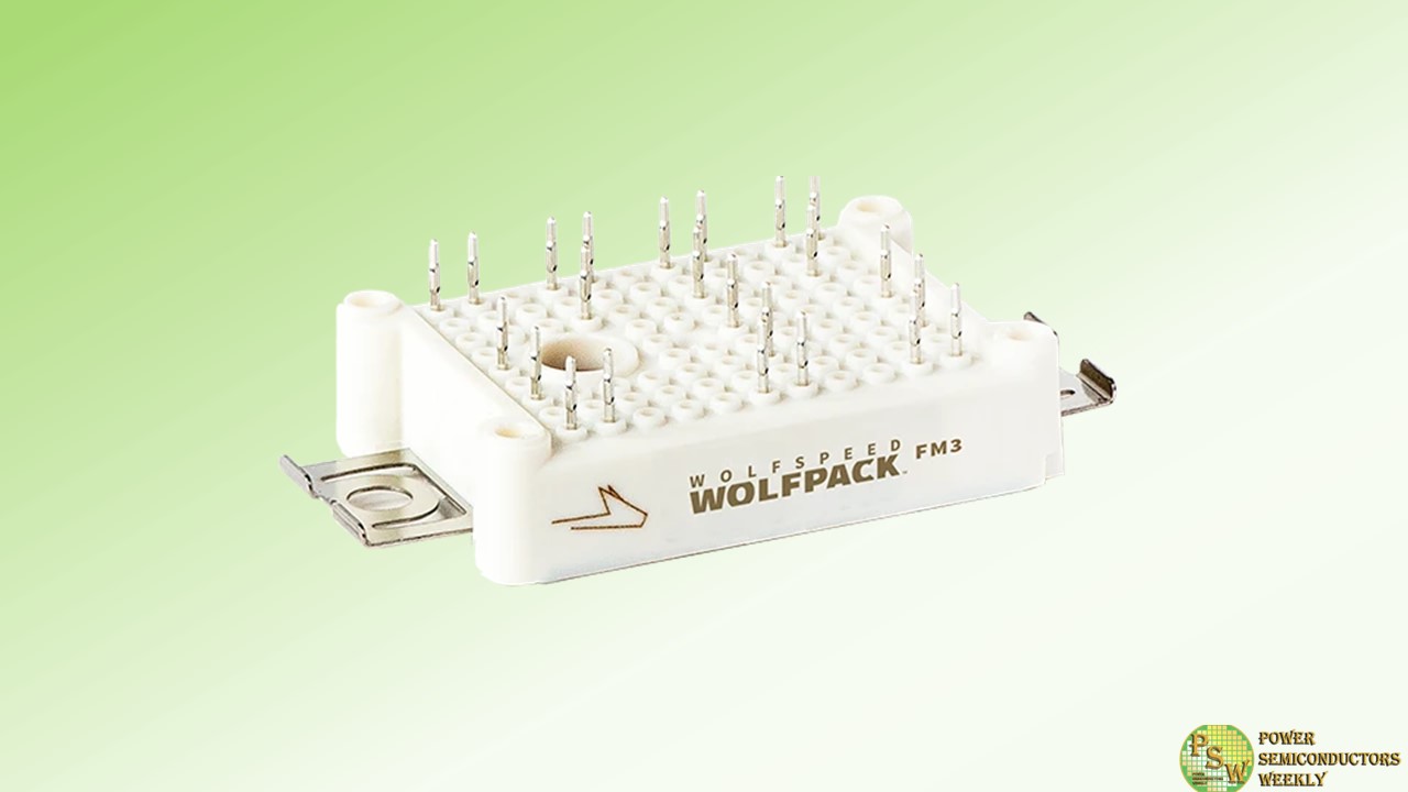
The Wolfspeed WolfPACK power module family is designed to give engineers choice and flexibility when working on power electronics applications greater than 10 kW.
In addition to half-bridge and six-pack topologies, WolfPACK modules are now available in full-bridge configurations—all with the option for pre-applied Honeywell™ PTM6000 Series TIM.
Selecting pre-applied TIM can reduce assembly cost and complexity, while improving reliability and performance. Compared to standard grease solutions, WolfPACK modules with pre-applied TIM can reduce the junction temperature by 40°C under the same conditions or increase current capability by 60% due to the reduction in thermal resistance.
All WolfPACK modules are designed to provide clean, reliable power for energy conversion systems. By leveraging more than 35 years of vertically integrated industry experience, Wolfspeed ensures that these modules offer low losses in a package that lends itself to fast design implementation, scalability, long term design support, and lower assembly overhead.
Original – Wolfspeed
-

Hitachi, Ltd. has signed an agreement to transfer all shares of its wholly owned subsidiary, Hitachi Power Semiconductor Device, to MinebeaMitsumi Inc. for further growth and corporate value enhancement of Hitachi Power Semiconductor Device.
Hitachi Power Semiconductor Device was established in October 2013 for the purpose of structuring an integrated system from design and manufacturing to sales in power semiconductor business by integrating the business of Hitachi and Hitachi Haramachi Electronics Co.
Since then, Hitachi Power Semiconductor Device has been providing high value-added products utilizing high-voltage and low-loss technologies in the field of power semiconductors, which are key devices in the electrification and motorization of industry and social infrastructure, with “IGBT/SiC”, “High Voltage IC” and ” Diodes” as its three main product categories. Hitachi Power Semiconductor Device is focusing on IGBT/SiC products in the market areas where high growth is expected toward the realization of a decarbonized society, such as electric vehicles and inverters for wind power generators, in addition to railroad applications, utilizing the strength of the high durability and reliability cultivated in railroad applications.
Many customers in Japan and overseas have adopted IGBT/SiC made by Hitachi Power Semiconductor Device. In the area of high-voltage ICs for industrial and home appliance applications, Hitachi Power Semiconductor Device is contributing to efficiency improvement and noise reduction in customers’ systems through motor control technology and software based on the knowledge it has gained from providing products for a wide range of fields. Furthermore, Hitachi Power Semiconductor Device provides diodes for automotive applications, which require high reliability, for a long period of time.
Hitachi and Hitachi Power Semiconductor Device have held many discussions on measures to achieve further growth and enhance the corporate value of Hitachi Power Semiconductor Device. As a result of the discussion, we have reached a conclusion that the best way for Hitachi Power Semiconductor Device to continue its growth in the power semiconductor market, which is expected a high growth in the future, is to expand its production capacity and improve manufacturing efficiency under MinebeaMitsumi, which positions the analog semiconductor business as one of its core businesses.
Under MinebeaMitsumi, with whom Hitachi Power Devices has been collaborating for many years, Hitachi Power Semiconductor Device will further enhance its strengths in high-voltage, low-loss technologies, expand its production capacity and improve manufacturing efficiency to provide higher value-added products in larger quantities to markets and customers, thereby aiming for further growth and corporate value enhancement.
Hitachi will strive to further enhance its corporate value by leveraging the funds obtained from this share transfer for investment in growth of green and service business in the energy field.
Original – Hitachi
-

Texas Instruments (TI) broke ground on its new 300-mm semiconductor wafer fabrication plant (or “fab”) in Lehi, Utah. Joined by Utah Governor Spencer Cox, state and local elected officials, as well as community leaders, TI President and Chief Executive Officer Haviv Ilan celebrated the first steps toward construction of the new fab, LFAB2, which will connect to the company’s existing 300-mm wafer fab in Lehi. Once completed, TI’s two Utah fabs will manufacture tens of millions of analog and embedded processing chips every day at full production.
“Today we take an important step in our company’s journey to expand our manufacturing footprint in Utah. This new fab is part of our long-term, 300-mm manufacturing roadmap to build the capacity our customers will need for decades to come,” said Ilan. “At TI, our passion is to create a better world by making electronics more affordable through semiconductors. We are proud to be a growing member of the Utah community, and to manufacture analog and embedded processing semiconductors that are vital for nearly every type of electronic system today.”
In February, TI announced its $11 billion investment in Utah, marking the largest economic investment in state history. LFAB2 will create approximately 800 additional TI jobs as well as thousands of indirect jobs, with first production available as early as 2026.
“TI’s growing manufacturing presence in Utah will be transformative for our state, creating hundreds of good-paying jobs for Utahns to manufacture critically important technology,” said Utah Governor Spencer Cox. “We are proud that semiconductors – made in Utah by Utahns – will power the innovation that is foundational to our country’s economic and national security.”
As part of TI’s commitment to education, the company will invest $9 million dollars in the Alpine School District to develop the state’s first Science, Technology, Engineering and Math (STEM) learning community for all students in kindergarten through 12th grade. The multiyear program will embed STEM concepts more deeply into coursework for the district’s 85,000 students and provide STEM-oriented professional development for its teachers and administrators. The district-wide program will equip students with essential STEM skills, such as critical thinking, collaboration and creative problem-solving to succeed after graduation.
“We are excited this partnership will help our students develop essential knowledge and skills, preparing them for success in life and possible careers in the technology sector,” said Alpine School District Superintendent, Dr. Shane Farnsworth. “Working together with the city of Lehi, Texas Instruments, and our schools, this collaborative investment will impact students and their families for many generations to come.”
TI has a long-standing commitment to responsible, sustainable manufacturing. LFAB2 will be one of the company’s most environmentally efficient wafer fabs, designed to meet one of the Leadership in Energy and Environmental Design (LEED) building rating system’s highest levels of structural efficiency and sustainability: LEED Gold version 4.
LFAB2 has a goal to be powered by 100% renewable electricity, and advanced 300-mm equipment and processes in Lehi will further reduce waste, water and energy consumption. In fact, LFAB2 is expected to recycle water at nearly twice the rate of TI’s existing fab in Lehi.
LFAB2 will complement TI’s existing 300-mm wafer fabs, which include LFAB1 (Lehi, Utah), DMOS6 (Dallas), and RFAB1 and RFAB2 (both in Richardson, Texas). TI is also building four new 300-mm wafer fabs in Sherman, Texas (SM1, SM2, SM3 and SM4), with production from the first fab as early as 2025.
TI’s manufacturing expansions, with anticipated support from the CHIPS and Science Act, will provide reliable supply of analog and embedded processing products. These investments in manufacturing and technology illustrate the company’s commitment to long-term capacity planning.
Original – Texas Instruments
-

Power Integrations released the world’s highest-voltage, single-switch gallium-nitride (GaN) power supply IC, featuring a 1250-volt PowiGaN™ switch. InnoSwitch™3-EP 1250 V ICs are the newest members of Power Integrations’ InnoSwitch family of off-line CV/CC QR flyback switcher ICs, which feature synchronous rectification, FluxLink™ safety-isolated feedback and an array of switch options: 725 V silicon, 1700 V silicon carbide, and PowiGaN in 750 V, 900 V and now 1250 V varieties.
The switching losses for Power Integrations’ proprietary 1250 V PowiGaN technology are less than a third of that seen in equivalent silicon devices at the same voltage. This results in power conversion efficiency as high as 93 percent – enabling highly compact flyback power supplies that can deliver up to 85 W without a heatsink.
Radu Barsan, vice president of technology at Power Integrations, said: “Power Integrations continues to advance the state of the art in high-voltage GaN technology development and commercial deployment, rendering even the best high-voltage silicon MOSFETs obsolete along the way. We were first to market with high-volume shipments of GaN-based power-supply ICs in 2019, and earlier this year introduced a 900-volt version of our GaN-based InnoSwitch products.
Our ongoing development of higher voltage GaN technology, illustrated here by our new 1250 V devices, extends the efficiency benefits of GaN to an even wider range of applications, including many currently served by silicon-carbide technology.”
Designers using the new InnoSwitch3-EP 1250 V ICs can confidently specify an operating peak voltage of 1000 V, which allows for industry-standard 80 percent de-rating from the 1250 V absolute maximum. This provides significant headroom for industrial applications and is particularly valuable in challenging power grid environments where robustness is an essential defense against grid instability, surge and other power perturbations.
Original – Power Integrations
-
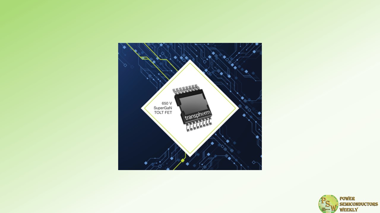
Transphorm, Inc. introduced the SuperGaN® TOLT FET. With an on-resistance of 72 milliohms, the TP65H070G4RS transistor is the industry’s first top-side cooled surface mount GaN device in the JEDEC-standard (MO-332) TOLT package. The TOLT package offers flexibility of thermal management to customers where system requirements do not allow for the more conventional surface mount devices with bottom-side cooling.
The thermal performance of the TOLT is similar to that of the widely used, thermally robust TO-247 through-hole packages and delivers the added benefit of highly efficient manufacturing processes enabled by SMD-based printed circuit board assembly (PCBA).
The TP65H070G4RS leverages Transphorm’s robust, high performance 650-volt normally-off d-mode GaN platform offering improved efficiency over silicon, silicon carbide, and other GaN offerings via lower gate charge, output capacitance, crossover loss, reverse recovery charge, and dynamic resistance.
The SuperGaN platform advantages combined with the TOLT’s better thermals and system assembly flexibility results in a high performance, high reliability GaN solution for customers seeking to bring to market power systems with higher power density and efficiency at an overall lower power system cost.
Transphorm is engaged with multiple global partners for high power GaN, including lead customers in server and storage power, a global leader in the energy/microinverter space, an innovative manufacturer of off-grid power solutions, and a leader in satellite communications.
“Surface mount devices such as the TOLL and the TOLT offer various benefits such as lower internal inductance as well as simpler board mounting during manufacturing. The TOLT adds to that more flexible overall thermal management with through-hole like thermal performance by using top-side cooling,” said Philip Zuk, SVP Business Development and Marketing, Transphorm.
“These devices are commonly found in mid to high power system applications for key market segments including high performance computing (Server, Telecom, AI Power), Renewables and Industrial, and Electric Vehicles, some of which our GaN technology already powers today. we’re very excited to enable our customers to realize additional system level benefits with TOLT SuperGaN solutions.”
Today’s product release comes on the heels of Transphorm’s recent introduction of its three new TOLL FETs. Addition of the TOLT expands the company’s product offerings yet again. Its availability highlights Transphorm’s commitment to supporting customer preferences by making its SuperGaN platform accessible in various packages across the widest power range.
Device Specifications
SuperGaN devices lead the market with unmatched:- Reliability at < 0.05 FIT
- Gate safety margin at ± 20 V
- Noise immunity at 4 V
- Temperature coefficient of resistance (TCR) at 20% lower than e-mode normally-off GaN
- Drive flexibility with standard off-the-shelf silicon drivers
The robust 650 V SuperGaN TOLT device is JEDEC qualified. Because the normally-off d-mode platform pairs the GaN HEMT with an integrated low voltage silicon MOSFET, the SuperGaN FETs are easy to drive with commonly used off-the-shelf gate drivers. They can be used in various hard- and soft-switching AC-to-DC, DC-to-DC, and DC-to-AC topologies to increase power density while reducing system size, weight, and overall cost.
Part Dimensions (mm) RDS(on) (mΩ) typ RDS(on) (mΩ) max Vth (V) typ Id (25°C) (A) max TP65H070G4RS 10 x 15 72 85 4 29 Original – Transphorm
-
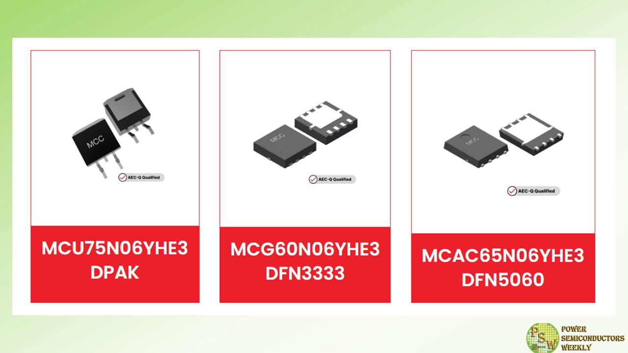
MCC Semi expanded its growing auto-grade portfolio with three new 60V N-channel MOSFETs: MCU75N06YHE3-TP, MCG60N06YHE3-TP, and MCAC65N06YHE3-TP.
Leveraging split-gate trench (SGT) MOSFET technology, MCC’s new products deliver optimal performance, efficiency, and thermal management, making them the intelligent choice for a range of demanding auto applications.
With on-resistance as low as 4.8mΩ, these AEC-Q101 qualified MOSFETs guarantee optimal power flow while significantly reducing power losses.
DFN333, DFN5060, and DPAK package options enable design flexibility and compatibility with various automotive systems.
Original – Micro Commercial Components
-
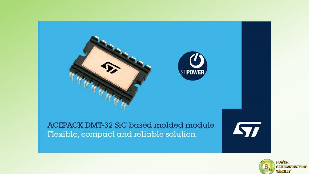
STMicroelectronics has released the ACEPACK DMT-32 family of silicon carbide (SiC) power modules in a convenient 32-pin, dual-inline, molded, through-hole package for automotive applications. Targeted at systems such as on-board chargers (OBC), DC/DC converters, fluid pumps and air conditioning, they deliver advantages including high power density, very compact design, and simplified assembly. The product family enhances flexibility for system designers by presenting a choice of four-pack, six-pack, and totem-pole configurations.
The modules contain 1200V SiC power switches that leverage ST’s state-of-the-art, second- and third-generation SiC MOSFET technology ensuring low RDS(on) values. The devices deliver efficient switching performance with minimal dependence on temperature to ensure high efficiency and reliability at converter system level.
Leveraging ST’s proven, robust ACEPACK technology, the modules reduce overall system- and design-development costs while ensuring outstanding reliability. The package technology features a high-performance aluminum nitride (AlN) insulated substrate for excellent thermal performance. There is also an integrated NTC sensor that provides temperature monitoring for thermal protection.
The first product in ACEPACK DMT-32, introduced today with ramp-up to volume production since Q4’23, is M1F45M12W2-1LA. The M1F80M12W2-1LA, M1TP80M12W2-2LA, M1P45M12W2-1LA, M1P80M12W2-1LA, M1P30M12W3-1LA are sampling now with ramp-up to volume production starting from Q1’24.
Original – STMicroelectronics
-
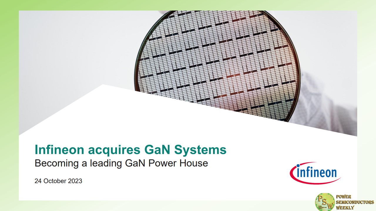
Infineon Technologies AG announced the closing of the acquisition of GaN Systems Inc. (“GaN Systems”). The Ottawa-based company brings with it a broad portfolio of gallium nitride (GaN)-based power conversion solutions and leading-edge application know-how. All required regulatory clearances have been obtained and GaN Systems has become part of Infineon effective as of the closing.
“GaN technology is paving the way for more energy-efficient and CO 2-saving solutions that support decarbonization,” said Jochen Hanebeck, CEO of Infineon. “The acquisition of GaN Systems significantly accelerates our GaN roadmap and further strengthens Infineon’s leadership in power systems through mastery of all relevant power semiconductor technologies. We welcome our new colleagues from GaN Systems to Infineon.”
Infineon now has a total of 450 GaN experts and more than 350 GaN patent families, which expands the company’s leading position in power semiconductors and considerably speeds up time-to-market. Both companies’ complementary strengths in IP and application understanding as well as a well-filled customer project pipeline put Infineon in an excellent position to address various fast-growth applications.
On 2 March 2023, Infineon and GaN Systems announced that the companies had signed a definitive agreement under which Infineon would acquire GaN Systems for US$830 million. The acquisition, an all-cash transaction, was funded from existing liquidity.
Original – Infineon Technologies
-

onsemi announced the completed expansion of its state-of-the-art, world-largest silicon carbide (SiC) fabrication facility in Bucheon, South Korea. At full capacity, this fab will be able to manufacture more than one million 200 mm SiC wafers per year.
To support the ramp in SiC manufacturing capacity, onsemi plans to hire up to 1,000 local employees over the next three years to fill the mostly highly technical positions – a more than 40% increase over the present workforce of about 2,300.
Silicon carbide devices are a critical component for power conversion in electric vehicles (EVs), energy infrastructure and high-power EV chargers. The rapidly growing demand for these products has created a surge in demand for SiC chips, with demand outpacing supply for the foreseeable future. The expansion of the Bucheon fab addresses the pressing need for additional production capacity, allowing onsemi to continue to provide supply assurance for its customers and strengthen its leadership in intelligent power solutions.
Construction of the new advanced 150 mm/200 mm SiC fab line along with the high-tech utility building and adjacent parking garage began in the middle of 2022 and was completed in September 2023. The expansion of the 150 mm/200 mm SiC Epi and wafer fab emphasizes onsemi’s focus on building out its vertically integrated silicon carbide manufacturing supply chain at brownfield locations. The Bucheon SiC line is starting with the production of 150 mm wafers and will be converted to 200 mm in 2025 upon qualification of the 200 mm SiC process.
onsemi’s leadership was joined by a delegation of dignitaries led by Vice Governor for Economy of the Gyeonggi-Do Taeyoung Yeom; followed by Bucheon City Mayor YongEek Cho; National Assembly delegates; and Bucheon Chamber of Commerce and Industry Chairman JongHuem Kim. Also in attendance were representatives from local communities, customers, suppliers and the semiconductor industry.
onsemi CEO Hassane El-Khoury opened the event, noting, “The 150 mm/200 mm SiC wafer fab in Bucheon is critical to the continued success of our fully integrated SiC supply chain, enabling us to support the acceleration of electrification globally. The last five years have shown what extraordinary performance our Bucheon team is capable of, and what we can achieve when we work together with governmental agencies toward the common goal of a more sustainable future.”
“I am truly impressed by onsemi’s diligent and yet fast execution of its strategic plan to expand the Bucheon SiC wafer fab,” said Bucheon City Mayor YongEek Cho. “Not only will the city of Bucheon benefit from the creation of new employment opportunities in technology, but it will also be a part of laying the foundation for a sustainable ecosystem through electrification.”
Original – onsemi
-
 LATEST NEWS / PROJECTS / TOP STORIES
Samsung Electronics to Provide Service Across a Variety of Solutions, Including Power Semiconductors
October 19, 2023
3 Min ReadSamsung Electronics hosted Samsung Foundry Forum (SFF) 2023 Europe and unveiled its advanced and wide ranging automotive process solutions, from the most advanced 2-nanometer process to the 8-inch legacy process.
Alongside its customers and Samsung Advanced Foundry Ecosystem (SAFE) partners, Samsung Electronics showcased the latest technological trends and its business strategy tailored to the European market.
“Samsung Foundry is driving innovation in next-generation solutions to build an expanded portfolio that meets the growing needs of our automotive customers, especially as the era of electric vehicles becomes a reality,” said Dr. Siyoung Choi, President and Head of Foundry Business at Samsung Electronics. “We are strengthening our readiness to provide customers with distinguished service across a variety of solutions, including power semiconductors, microcontrollers and advanced AI chips for autonomous driving.”
Since participating in IAA Mobility 2023 for the first time in September, Samsung Electronics is strengthening engagement and partnership in specialty processes for automotive customers in the European market, further solidifying its status as a leading foundry partner for the industry.
Pioneering New Applications With Industry’s Most Advanced eMRAM
In order to meet the needs of the latest advancements in the automotive market, Samsung is setting out to develop the industry’s first 5-nanometer eMRAM for next-generation automotive technology. eMRAM is a next-generation memory semiconductor used for automotive applications that enables high read and write speeds as well as superior heat resistance.
Since developing and mass producing the industry’s first 28nm FD-SOI based eMRAM in 2019, Samsung Electronics has been developing 14nm for the FinFET process based on AEC-Q100 Grade 1. Samsung Foundry plans to expand its eMRAM portfolio by adding 14nm by 2024, 8nm by 2026, and 5nm by 2027.
Samsung’s 8nm eMRAM shows potential to deliver a 30% increase in density and 33% increase in speed, compared to the 14nm process.
Tackling the Market With Automotive Process Solutions From Cutting-Edge to Legacy
The company announced its advanced process roadmap, highlighting its plans to complete mass production readiness for its 2nm process for automotive applications by 2026.
Samsung Electronics is also bolstering its readiness to serve customer needs by expanding its 8-inch BCD (Bipolar-CMOS-DMOS) process portfolio. The BCD process combines the strengths of three different process technologies: Bipolar (B), CMOS (C), and DMOS (D) on one chip and is most commonly used in the production of power semiconductors.
Samsung Electronics plans to expand its current 130nm automotive BCD process to add 90nm by 2025. The 90nm BCD process is expected to bring a 20% decrease in chip area compared to the 130nm process.
Implementing Deep Trench Isolation (DTI) technology, which reduces the distance between each transistor to maximize the performance of power semiconductors, Samsung Foundry will be able to apply a greater voltage of 120V instead of 70V to a wider range of applications. This will enable readiness to provide a process development kit (PDK) that implements 120V to the 130nm BCD process by 2025.
Leading ‘Beyond-Moore’ Innovation Through Advanced Packaging Alliance
Samsung established a Multi-Die Integration (MDI) Alliance by collaborating with its SAFE partners as well as major players in memory, package substrate, and testing.
As part of an industry-wide partnership with 20 partners, Samsung is leading the development of 2.5D and 3D packaging solutions customized for all applications from automotive to high-performance computing (HPC).
Samsung Electronics hosted the annual Samsung Foundry Forum 2023 in the United States on June 27-28, in South Korea on July 4, and in Japan on October 17. The content from the forum will be available on the Samsung Semiconductor website for worldwide access to all visitors beginning November 2.
Original – Samsung Electronics
