-
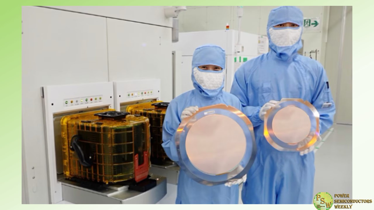
Mitsubishi Electric Corporation has completed installation of its first 12-inch silicon wafer processing line at its Power Device Work’s Fukuyama Factory, which manufactures power semiconductors. In addition, through sample production and testing, it has been verified that the power semiconductor chips processed on this production line achieve the required performance levels.
As previously announced, Mitsubishi Electric is planning to start mass production on the new 12-inch silicon wafer line in fiscal 2025. The company aims to approximately double its silicon power semiconductor wafer processing capacity by fiscal 2026 compared to fiscal 2021 levels.
In recent years, the demand for power semiconductors offering efficient control of electrical power is growing as countries look to achieve carbon-free status. Power semiconductors are utilized in wide range of relevant products, including electric vehicles, consumer devices (e.g. air-conditioning systems), industrial equipment, renewable energy and traction devices, and a stable supply is required in order to meet this growing demand.
Mitsubishi Electric will contribute to the realization of a carbon-free society through enhancement of its production capacity and by ensuring a stable supply of power semiconductors through the introduction of highly efficient 12-inch wafer production lines.
Original – Mitsubishi Electric
-
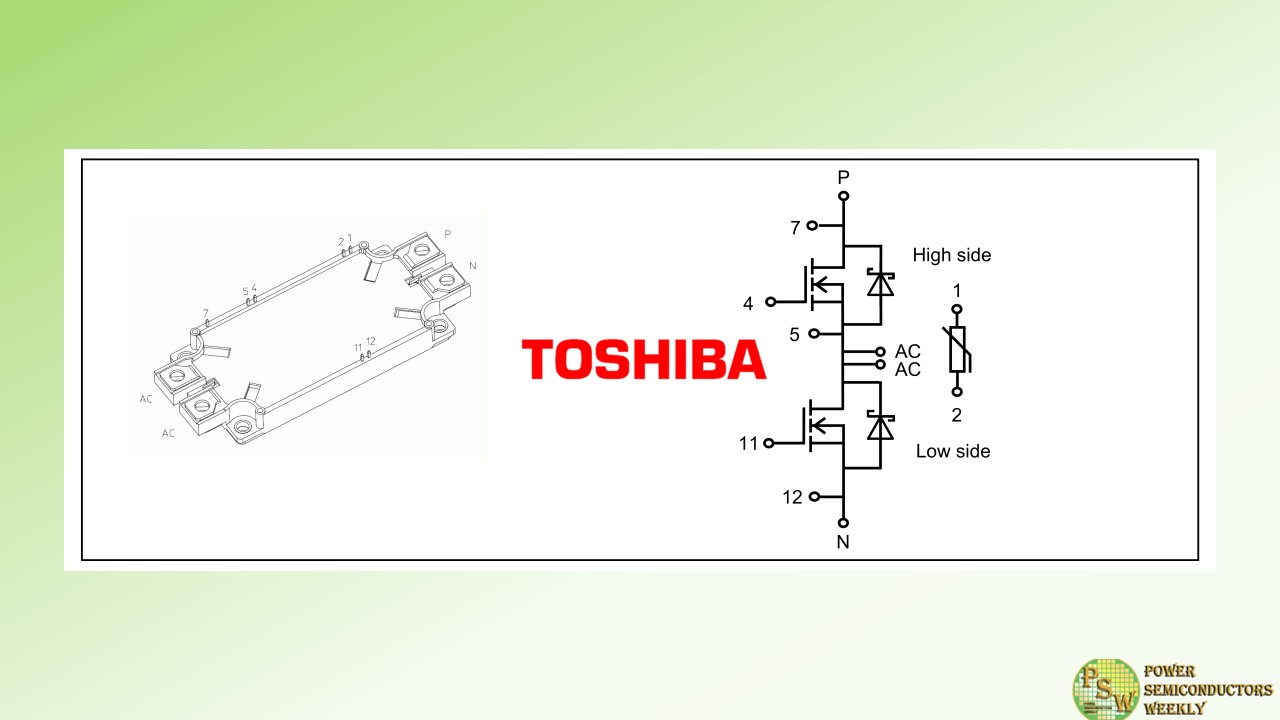
Toshiba Electronic Devices & Storage Corporation developed “MG250YD2YMS3,” the industry’s first 2200V dual silicon carbide (SiC) MOSFET module for industrial equipment. The new module has a drain current (DC) rating of 250A and uses the company’s third generation SiC MOSFET chips. It is suitable for applications that use DC1500V, such as photovoltaic power systems and energy storage systems. Volume shipments start today.
Industrial applications like those mentioned above generally use DC1000V or lower power, and their power devices are mostly 1200V or 1700V products. However, anticipating widespread use of DC1500V in coming years, Toshiba has released the industry’s first 2200V product.
MG250YD2YMS3 offers low conduction loss with a low drain-source on-voltage (sense) of 0.7V (typ.). It also offers lower turn-on and turn-off switching loss of 14mJ (typ.) and 11mJ (typ.) respectively, an approximately 90% reduction against a typical silicon (Si) IGBT. These characteristics contribute to higher equipment efficiency. Realizing low switching loss also allows the conventional three-level circuit to be replaced with a two-level circuit with a lower module count, contributing to equipment miniaturization.
Toshiba will continue to meet the market needs for high efficiency and the downsizing of industrial equipment.
Applications
Industrial Equipment
- Renewable energy power generation systems (photovoltaic power systems, etc.)
- Energy storage systems
- Motor control equipment for industrial equipment
- High frequency DC-DC converter, etc.
Features
- Low drain-source on-voltage (sense):
VDS(on)sense=0.7V (typ.) (ID=250A, VGS=+20V, Tch=25°C) - Low turn-on switching loss:
Eon=14mJ (typ.) (VDD=1100V, ID=250A, Tch=150°C) - Low turn-off switching loss:
Eoff=11mJ (typ.) (VDD=1100V, ID=250A, Tch=150°C) - Low stray inductance:
LsPN=12nH (typ.)
Original – Toshiba
-
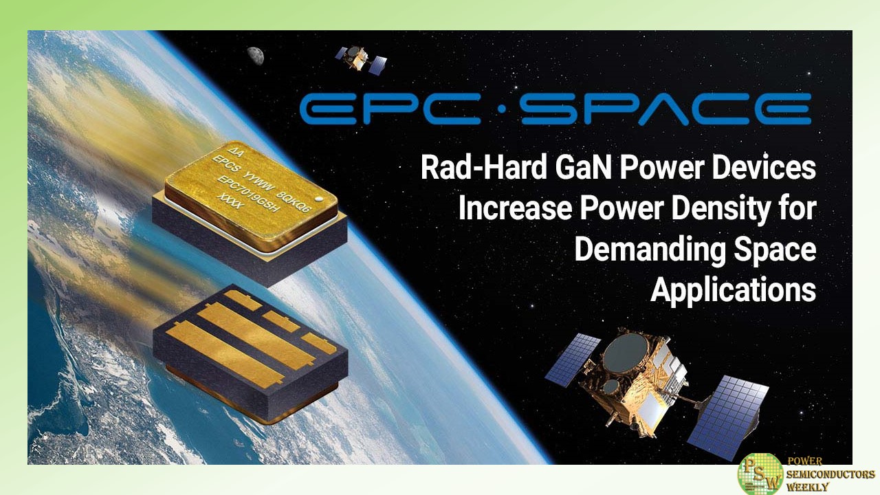
EPC Space announced the introduction of two new rad-hard GaN transistors with ultra-low on-resistance and high current capability for high power density solutions that are lower cost and more efficient than the nearest comparable radiation-hardened silicon MOSFET. These devices come packaged in hermetic packages in very small footprints.
The EPC7020G is a 200 V, 14.5 mΩ, 200 Apulsed radiation-hardened gallium nitride transistor and the EPC7030G is a 300 V, 32 mΩ, 200 Apulsed radiation-hardened gallium nitride transistor. These devices join the 40 V, 4.5 mΩ EPC7019G and the 100 V, 4.5 mΩ EPC7018G to cover applications including power supplies for satellites and space mission equipment, motor drives for robotics, instrumentation and reaction wheels, and deep space probes. This product family comes packaged in a compact hermetic package in a footprint less than 45 mm2.
Part Number Drain to Source Voltage (VDS) Drain to Source Resistance (RDS(on)) Single-Pulse Drain Current (IDM) EPC7019G 40 V 4 mΩ 530 A EPC7018G 100 V 6 mΩ 345 A EPC7020G 200 V 14.5 mΩ 200 A EPC7030G 300 V 32 mΩ 200 A With higher breakdown strength, lower gate charge, lower switching losses, better thermal conductivity, and lower on-resistance, power devices based on GaN significantly outperform silicon-based devices and enable higher switching frequencies resulting in higher power densities, higher efficiencies, and more compact and lighter weight circuitry for critical spaceborne missions.
“The G-Package family offers the lowest on-resistance of any packaged rad hard transistor currently on the market,” said Bel Lazar, CEO of EPC Space. “These devices offer mission-critical components with superior figure of merit, significantly smaller size, and lower cost for the space and other high-reliability markets than alternative rad hard silicon solutions”.
Original – EPC Space
-
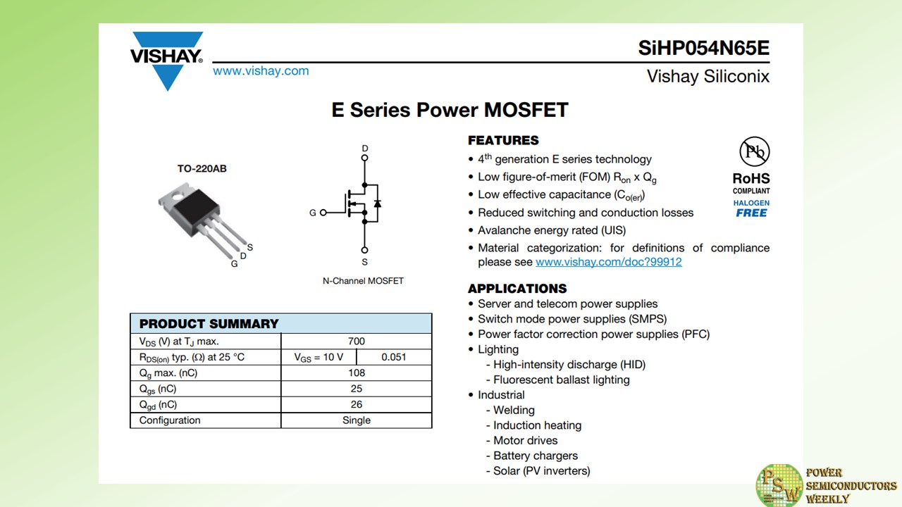
Vishay Intertechnology, Inc. introduced a new fourth-generation 650 V E Series power MOSFET that delivers high efficiency and power density for telecom, industrial, and computing applications. Compared to previous-generation devices, the Vishay Siliconix n-channel SiHP054N65E slashes on-resistance by 48.2 %, while offering a 59 % lower resistance times gate charge, a key figure of merit (FOM) for 650 V MOSFETs used in power conversion applications.
Vishay offers a broad line of MOSFET technologies that support all stages of the power conversion process, from high voltage inputs to the low voltage outputs required to power the latest high tech equipment. With the SiHP054N65E and other devices in the fourth-generation 650 V E Series family, the company is addressing the need for efficiency and power density improvements in two of the first stages of the power system architecture — power factor correction (PFC) and subsequent DC/DC converter blocks.
Typical applications will include servers, edge computing, and data storage; UPS; high intensity discharge (HID) lamps and fluorescent ballast lighting; solar inverters; welding equipment; induction heating; motor drives; and battery chargers.
Built on Vishay’s latest energy-efficient E Series superjunction technology, the SiHP054N65E’s low typical on-resistance of 0.051 Ω at 10 V results in a higher power rating for applications > 2 kW and allows the device to address the Open Compute Project’s Open Rack V3 (ORV3) standards. In addition, the MOSFET offers ultra low gate charge down to 72 nC. The resulting FOM of 3.67 Ω*nC is 1.1 % lower than the closest competing MOSFET in the same class, which translates into reduced conduction and switching losses to save energy and increase efficiency. This allows the device to address the specific titanium efficiency requirements in server power supplies or reach 96 % peak efficiency in telecom power supplies.
For improved switching performance in hard-switched topologies such as PFC, half-bridge, and two-switch forward designs, the MOSFET released today provides low typical effective output capacitances Co(er) and Co(tr) of 115 pF and 772 pF, respectively. The device’s resulting resistance times Co(er) FOM is an industry-low 5.87 Ω*pF. Offered in the TO-220AB package and providing increased dv/dt ruggedness, the SiHP054N65E is RoHS-compliant, halogen-free, and Vishay Green, and is designed to withstand overvoltage transients in avalanche mode with guaranteed limits through 100 % UIS testing.
Original – Vishay Intertechnology
-

The Volkswagen Group is reorganizing its procurement of electronic parts and semiconductors to ensure supply over the long term and, in doing so, securing itself a leading position in terms of technology as well as competitiveness. To this end, the Group has developed a new strategy for the procurement of parts with electronic components.
“A high degree of transparency in the semiconductor value chain – the exact knowledge of the parts used – enables us to better determine the global demand and availability of these components. This is underscored by risk management which, in future, will extend to the level of individual electronic parts and help us detect bottlenecks early on and avoid them.
For strategically important semiconductors and even the Group’s own planned developments in the future, we will rely on direct purchasing from the semiconductor manufacturers,” said Dirk Große-Loheide, Board Member for Procurement of Volkswagen Passenger Cars and member of Group management.
In the past, electronic components like control units were procured and the Tier 1 suppliers were largely free to decide which parts they used. Going forward, in close collaboration and partnership with Tier 1 suppliers, Group procurement will define which semiconductors and other electronic parts are to be used.
“Additionally, this is done across all brands by the Semiconductor Sourcing Committee (SSC) established especially for this purpose, with representatives from the procurement and development departments of the brands as well as from Volkswagen Group Components and CARIAD. Furthermore, the transparency regarding semiconductors means that technical alternatives can be identified and implemented more quickly in the event of bottlenecks.
Another positive effect is that a reduction in the diversity of variants in the hardware results in a lower degree of software complexity,” said Karsten Schnake, Board Member for Procurement at Škoda Auto and head of the cross-brand and cross-functional task force COMPASS (Cross Operational Management Parts & Supply Security), explaining the advantages.
Semiconductors are indispensable in the automotive industry: not only are they elementary for mass production, but they are also innovation drivers and key for launching new products on the market.
The greatest increase in demand for semiconductors is the result of the increasing electrification of vehicles and the trend towards the growing use of assistant functions through to fully autonomous driving. The corresponding innovations will also result in the use of cutting-edge semiconductors, while the demand for more common semiconductors will remain or even rise further. Vehicle innovations are heavily characterised by the use of semiconductors: in 1978, only eight semiconductors were installed in a control unit of a Porsche 911. Today, a Škoda Enyaq has around 90 control units with some 8,000 electronic components.
This development also has an impact on the value of electronic components in the vehicle, the value of which will more than double by the year 2030 from today’s average of around 600 euros per vehicle. According to the Group’s assessment and corresponding analyzes, the importance of the automotive sector as a customer of the semiconductor industry is also increasing.
Today, the automotive industry is in 5th place among the major buyers with a global procurement volume for semiconductors of around 47 billion US dollars. By 2030, our industry is expected to secure third place with a market volume of around 147 billion US dollars.
The after-effects of the COVID-19 pandemic and the associated chip crisis can still be felt. To solve these enormous challenges and ensure the semiconductor supply, the Volkswagen Group launched the COMPASS initiative at the beginning of 2022, initially with the operational focus of safeguarding the vehicle programme. Strategic action areas were identified on the basis of lessons learned during the semiconductor crisis and solutions were developed and implemented for the long term.
Original – Volkswagen
-
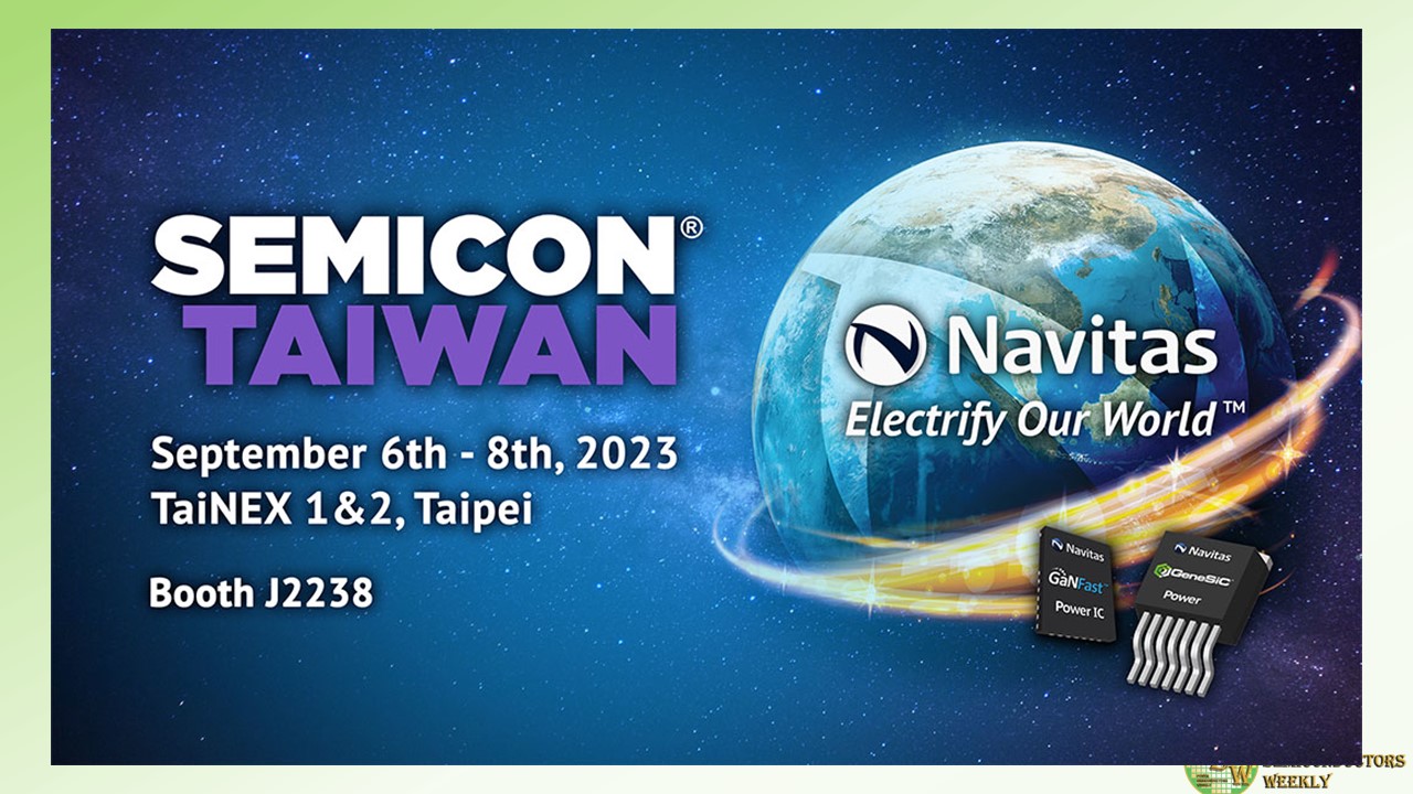
Navitas Semiconductor will reveal a new, high-performance wide bandgap power platform as part of its display at one of Asia’s most prestigious electronics exhibitions – sponsored by Navitas – SEMICON Taiwan 2023, from September 6th-8th.
Visitors will discover the latest gallium nitride (GaN) GaNFast™ power ICs integrate gallium nitride (GaN) power and drive, with control, sensing, and protection to enable faster charging, higher power density, and greater energy savings. Complementary GeneSiC™ power devices are optimized high-power, high-voltage, and high-reliability silicon carbide (SiC) solutions.
Additionally, Navitas will showcase cutting-edge, power-system platforms to dramatically accelerate customer developments, minimize time-to-market, and set new industry benchmarks in energy efficiency, power density and system cost. These system platforms include complete design collateral with fully-tested hardware, embedded software, schematics, bill-of-materials, layout, simulation and hardware test results. Examples include:
- Navitas’ CRPS185 data center power platform, that delivers a full 3,200 W of power in only 1U (40 mm) x 73.5mm x 185 mm (544 cc), achieving 5.9 W/cc, or almost 100 W/in3 power density. This is a 40% size reduction vs, the equivalent legacy silicon approach and reaches over 96.5% efficiency at 30% load, and over 96% stretching from 20% to 60% load, creating a ‘Titanium Plus’ benchmark.
- Navitas’ 6.6 kW 3-in-1 bi-directional EV on-board charger (OBC) with 3 kW DC-DC. This 96%+ efficient unit has over 50% higher power density, and with efficiency over 95%, delivers up to 16% energy savings as compared to competing solutions.
As part of SEMICON’s Power and Opto Semiconductor Forum, Navitas’ Charles Bailley, Senior Director of Business Development, will present “GaN Power ICs Increase Power Density in EV Power Systems”. The presentation is at 2pm, on September 6th, in room 402, 4F, TaiNEX 1.
“Breakthrough high efficiency, high reliability, and high power density – all from the new GaN power IC platform,” said Kevin 汪時民 Wang, Manager of Navitas Taiwan. “The new platform announcement matches SEMICON’s theme of ‘Innovating the World through Semiconductors’ and our own mission to ‘Electrify Our World™’.”
Original – Navitas Semiconductor
-
Toshiba Electronic Devices & Storage Corporation has launched three 80 V N-channel power MOSFET products that use its latest generation process “U-MOSX-H series” and are suitable for switching power supplies for industrial equipment—used for such as data centers and communication base stations—and expanded the lineup.
The new products use the surface mount type SOP Advance(N) package, and their drain-source On-resistance (max) is 3 mΩ for “TPH3R008QM”, 6 mΩ for “TPH6R008QM”, and 8.8 mΩ for “TPH8R808QM”.
The new products have reduced the figure of merits (FOMs: expressed as On-resistance × charge characteristics.) In case of TPH3R008QM, it has reduced its FOMs, drain-source On-resistance × total gate charge by approximately 48 %, drain-source On-resistance × gate switch charge by approximately 16 %, and drain-source On-resistance × output charge by approximately 33 %, compared to Toshiba’s existing product TPH4R008NH. This contributes to lowering power consumption of equipment.
Toshiba is expanding its lineup of products to help cut equipment power consumption.
Applications
- Switching power supplies (high efficiency AC-DC converters, high efficiency DC-DC converters, etc.)
- Motor control equipment (motor drives, etc.)
Features
- Latest generation process U-MOSX-H series
- Low On-resistance:
TPH3R008QM RDS(ON)=3 mΩ (max) (VGS=10 V)
TPH6R008QM RDS(ON)=6 mΩ (max) (VGS=10 V)
TPH8R808QM RDS(ON)=8.8 mΩ (max) (VGS=10 V) - High channel temperature: Tch (max)=175 °C
Original – Toshiba
-
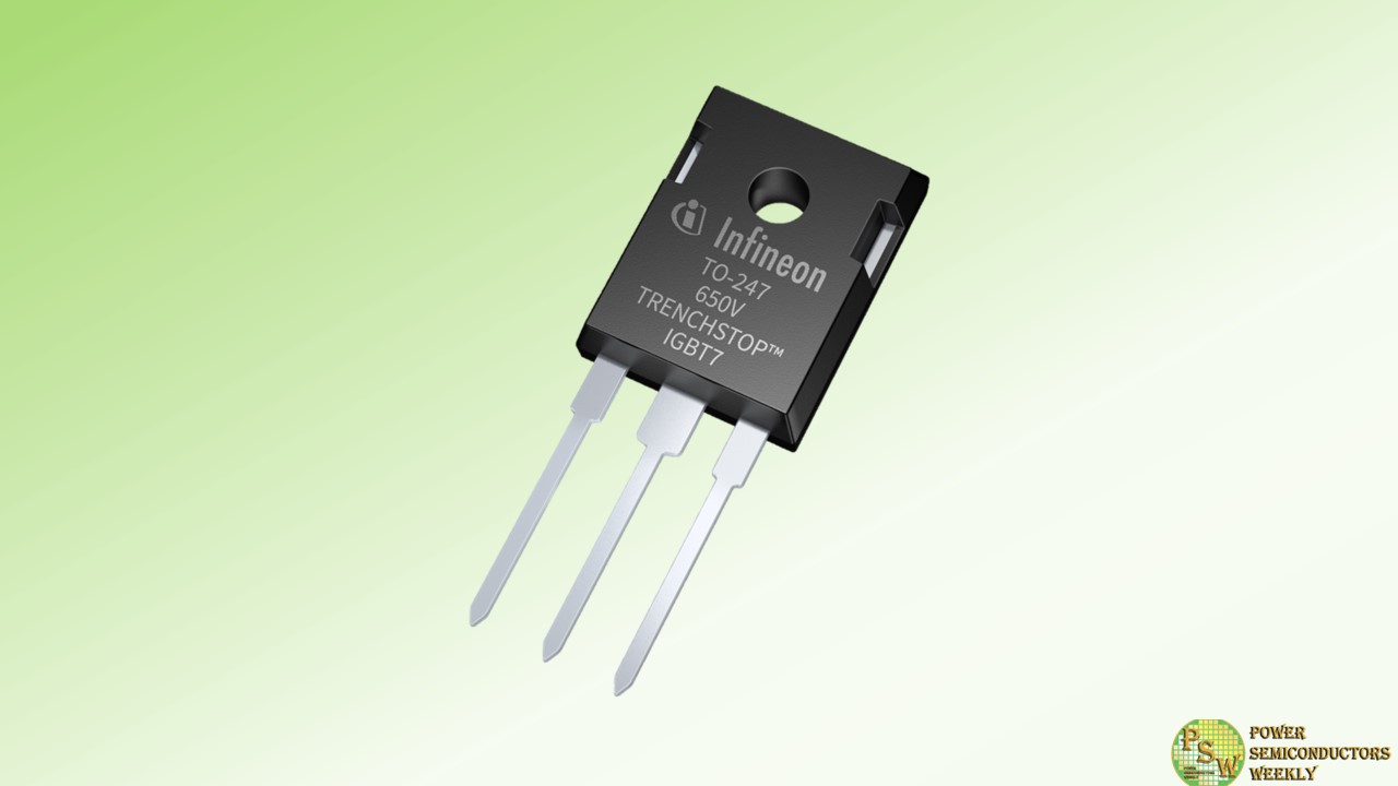
Infineon Technologies AG expands its 7th generation TRENCHSTOP™ IGBT family with the discrete 650 V IGBT7 H7 variant. The devices feature a cutting-edge EC7 co-packed diode with an advanced emitter-controlled design, coupled with high-speed technology to address the escalating need for environmentally conscious and highly efficient power solutions.
Using the latest micro-pattern trench technology, the TRENCHSTOP IGBT7 H7 offers excellent control and performance, resulting in significant loss reduction, improved efficiency and higher power density. As a result, the device is ideal for various applications such as string inverters, energy storage systems (ESS), electric vehicle charging applications, and traditional applications such as industrial UPS and welding.
In a discrete package, the 650 V TRENCHSTOP IGBT7 H7 can deliver up to 150 A. The portfolio includes variants from 40 A to 150 A, offered in four different package types: TO-247-3 HCC, TO-247-4, TO-247-3 Plus and TO-247-4 Plus. The TO-247-3 HCC variant of the TRENCHSTOP IGBT 7 H7 features a high creepage distance.
For improved performance, the TO-247 4-pin packages (standard: IKZA, Plus: IKY) are particularly well suited, as they not only reduce switching losses, but also offer additional benefits such as lower voltage overshoot, minimized conduction losses and the lowest reverse current loss. With these features, the TRENCHSTOP IGBT 7 H7 simplifies the design and minimizes the need to connect devices in parallel.
In addition, the 650 V TRENCHSTOP IGBT 7 H7 features robust moisture resistance for reliable operation in harsh environments. The device is qualified for industrial use according to the relevant tests of JEDEC47/20/22, especially HV-H3TRB, making it well suited for outdoor applications.
Designed to meet the demand for green and efficient power applications, the IGBT offers significant improvements over the previous generations. As a result, the TRENCHSTOP IGBT 7 H7 is the ideal complement for the NPC1 topology often used in applications such as solar and ESS.
Original – Infineon Technologies
-

MACOM Technology Solutions Holdings, Inc. announced that it has entered into a definitive agreement to acquire the radio frequency business of Wolfspeed, Inc. The RF Business includes a portfolio of Gallium Nitride (“GaN”) on Silicon Carbide (“SiC”) products used in high performance RF and microwave applications.
The business services a broad customer base of leading aerospace, defense, industrial and telecommunications customers and most recently generated annualized revenues of approximately $150 million. The acquisition is expected to be immediately accretive to MACOM’s non-GAAP earnings.
“We are excited to acquire Wolfspeed’s RF Business and look forward to welcoming its employees to MACOM,” stated Stephen G. Daly, President and Chief Executive Officer, MACOM. “The RF team’s engineering capabilities, technology and products are a perfect fit with MACOM and our strategy.”
The acquisition includes a 100mm GaN wafer fabrication facility in Research Triangle Park, North Carolina (the “RTP Fab”) with operations conveying to MACOM approximately two years following the closing and Wolfspeed’s relocation of certain production equipment.
The acquisition also includes design teams and associated product development assets in Arizona, California and North Carolina, as well as back-end production capabilities in California and Malaysia. In addition, MACOM will be assigned or licensed a robust intellectual property portfolio including over 1,400 patents associated with the RF Business.
The RF Business will be acquired for $125 million, including $75 million cash paid at closing and $50 million of MACOM common stock issued with certain restrictions. A workforce of approximately 280 employees is expected to join MACOM at closing, with additional employees joining when the RTP Fab conveys.
Closing of the transaction is subject to the expiration of a waiting period under the Hart-Scott-Rodino Antitrust Improvements Act of 1976 and other closing conditions and is expected to occur in the second half of calendar year 2023.
Original – MACOM Technology Solutions
-
The rapid growth of technology over the past century brought us as many advantages as many disadvantages including the accelerating global warming with its dramatic consequences we face every day in various parts of the Earth. So far no one found a solution how to stop this process, but there are many solutions how to slow it down.
Today we try to respond to this challenge with carbon neutrality initiatives launched in many countries across the globe. And one of the major steps in this green society program is the electrification of passenger and commercial vehicles.
Right now, companies have various approaches to vehicle electrification including mild-hybrid electric vehicles MHEV, full hybrid electric vehicles HEV, plug-in hybrid electric vehicles PHEV, battery electric vehicles BEV, and fuel-cell electric vehicle FCEV. What some time ago seemed like a big step forward is a reality we live in now.
And to make this dream come true became possible with the help of power semiconductors. For a long time, semiconductors were used in the automotive industry, and the evolution of power semiconductor materials pushed the transition to the electrification of vehicles. Electric vehicles’ performance and cost depend on the technical level of the motor control system.
Previously, silicon (Si) IGBT modules served as the heart of electronic control systems with their relatively high switching speed and low conduction loss. But with the growth of silicon carbide (SiC) technology, EVs step into the new era of electrification.
Silicon-based semiconductors have been dominating the market for many decades. No wonder, several generations of power electronics engineers were passing their knowledge and experience working with silicon semiconductors. Through time they have short-listed their preferred solutions produced by several companies.
Based on the current requirements for the improvement of battery life and dynamic performance of electric passenger and commercial vehicles, higher efficiency, and fewer parts and materials are required to further improve the power density of inverters and electric drive assemblies. All this becomes possible with the transition from Si to SiC power devices. But when it comes to the all-new silicon carbide semiconductors and the rapidly growing EV industry, many face difficulties to make the right choice of the silicon carbide devices available in the market.
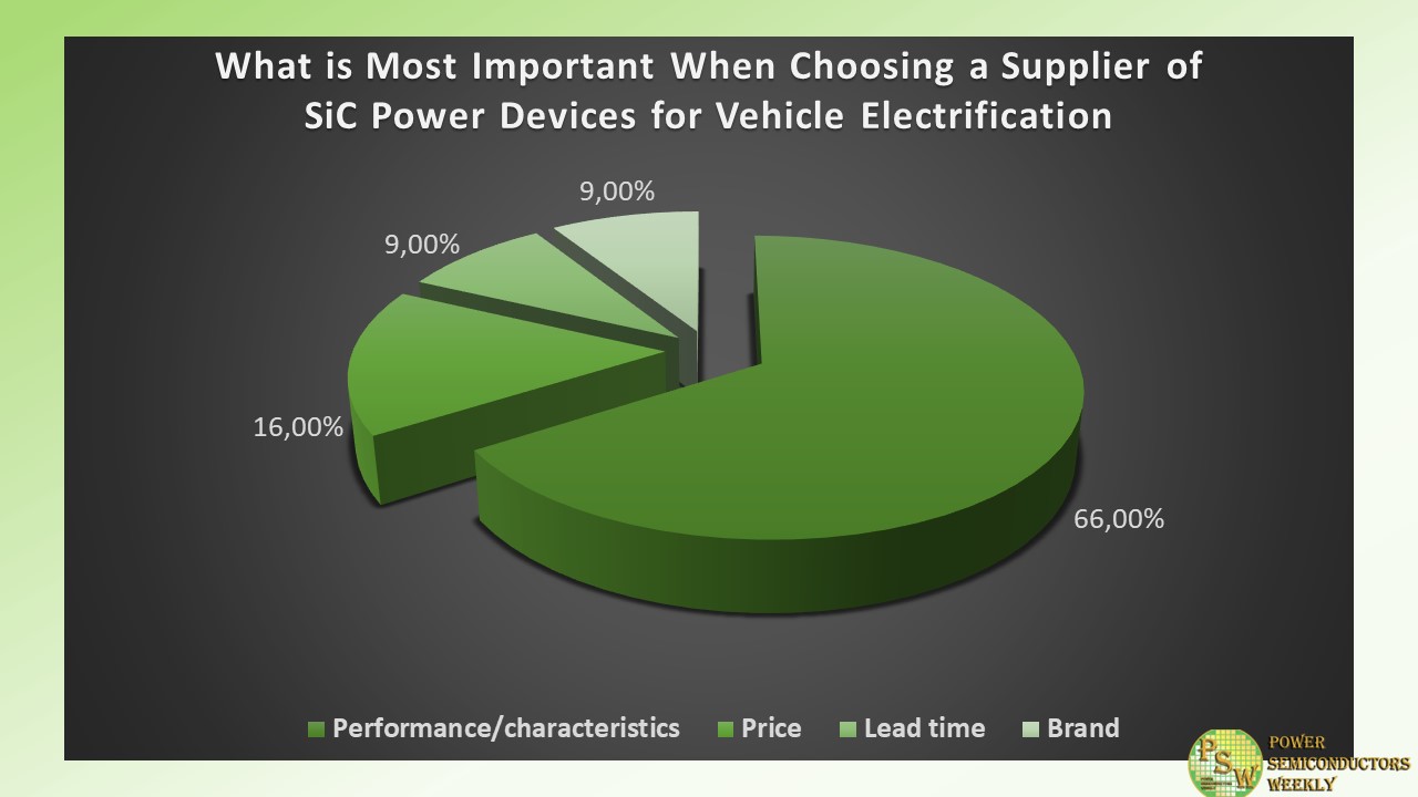
Recently I launched a poll to understand what is most important for EV companies when choosing a supplier of SiC power devices. Power electronics engineers from the semiconductor and automotive industries shared their experience and unanimously confirmed that the performance of the power devices plays a crucial role when choosing a supplier. The poll results are:
- Performance/characteristics – 66%
- Price – 16%
- Lead time – 9%
- Brand – 9%
Based on the results it is clear that for the EV market today characteristics of SiC power devices and price play the most important role. After all, consumers want high performance and reliability at affordable prices.
Nowadays SiC is still more expensive than Si. However, the prices have dropped a lot in the past decade, and the growing number of SiC fabs promises to drop the price in the future. Fingers crossed, in the nearest future, the dream of the consumers for the high-performance, reliable, and affordable EV will come true.
