-
Toshiba Electronic Devices & Storage Corporation has developed 2200 V silicon carbide (SiC) metal oxide semiconductor field effect transistors (MOSFETs) for photovoltaic (PV) inverters. A two-level inverter with the new devices realized higher frequency operation and lower power loss than a conventional three-level silicon (Si) insulated gate bipolar transistor (IGBT) inverter. The new MOSFETs also contribute to simplification of inverter systems and reductions in their size and weight.
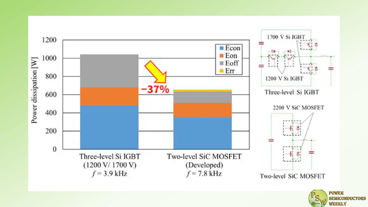
Three-level inverters enjoy the advantage of low switching losses because the voltage applied to switching devices in the inverters during off-state is half the line voltage. Against this, two-level inverters have fewer switching modules than three-level inverters, realizing a simpler, smaller, and lighter system. However, they require semiconductors with higher breakdown voltage, as the applied voltage is equal to the line voltage. Also, demand for semiconductors with both low loss and high breakdown voltage is growing as 1500 V DC line voltage systems are introduced in photovoltaic and other renewable energy markets.
Toshiba Electronic Devices & Storage Corporation has developed 2200 V Schottky barrier diode (SBD)-embedded SiC MOSFETs for two-level inverters in 1500 V DC voltage systems. The impurity concentration and thickness of the drift layer has been optimized to maintain the same relationship between the on-resistance and the breakdown voltage as our existing products, and also to achieve high resistance to cosmic rays, a requirement for PV systems. It has also been confirmed that embedding SBDs clamped parasitic PN junctions between the p-base regions and the n-drift layer secure high reliability in reverse conduction.
Switching energy loss for the developed all-SiC module is far lower than for the Si module (Si IGBTs + Si fast recovery diodes) with the same 2000 V rated voltage class. Estimates of inverter power dissipation found that the developed SiC module achieves higher frequency operation twice that of a conventional Si IGBT, as well as a 37% lower loss for the two-level SiC inverter against the three-level Si inverter. The higher frequency operation enables downsizing and weight reduction of other system components, such as heat sinks and filters.
Original – Toshiba
-

The University of Arkansas has taken the next step to becoming a national leader in the United States’ semiconductor economy. Semiconductors, such as silicon, are essential materials in most electronic devices and advance performance in fields such as healthcare, national defense, computing and transportation.
This August, the university began construction on the national Multi-User Silicon Carbide Research and Fabrication Facility, or MUSiC. Capable of silicon or silicon carbide chip fabrication, this new semiconductor research and fabrication facility will enable the government, businesses of all sizes, and universities to prototype in silicon carbide, introducing a capability that does not presently exist in the U.S.
This unique facility will offer low-volume prototyping for high-volume manufacturing, bridging the gap between traditional university research and the needs of private industry. This will accelerate both workforce development and technological advancement in semiconductors by providing a single location where chips can be go from developmental research to prototyping, testing and fabrication.
Alan Mantooth, Distinguished Professor of electrical engineering at the U of A, is principal investigator for MUSiC. He stated that with MUSiC, the university could “begin training the next generation at a variety of degree levels to provide well-trained and educated talent for onshoring semiconductor manufacturing that domestic suppliers offshored in the late 90s and early 2000s. Our training will be equally applicable to silicon and silicon carbide and other materials.”
Construction coincides with the CHIPS America Summit on Aug. 17, an invitation-only event for research, industry and governmental leaders from across the nation to discuss CHIPS and Science Act semiconductor-related opportunities and the ways in which the U of A and the State of Arkansas are uniquely positioned to lead.
The summit will feature Director of External and Government Affairs for the U.S Department of Commerce’s CHIPS Program Office, Adrienne Elrod. U.S. Representative Steve Womack and Arkansas Secretary of Commerce Hugh McDonald will also participate.
In addition to the MUSiC facility, the U of A is also home to the first Energy Frontier Research Center in Arkansas, as part of a team of researchers who received $10.35 million from the U.S. Department of Energy. The Center for Manipulation of Atomic Ordering for Manufacturing Semiconductors is dedicated to investigating the formation of atomic orders in semiconductor alloys and their effects on various physical properties. This research program will enable reliable, cost-effective and transformative manufacturing of semiconductors.
Researchers at the U of A previously established the MonArk NSF Quantum Foundry to accelerate the development of quantum materials and devices. In collaboration with Montana State University, and other member universities, the foundry supports the study of 2-D materials — consisting of a single layer of bonded atoms — by aiding researchers and facilitating the exchange of ideas across academia and industry. The project leads the fabrication of 2-D material quantum devices and their characterization, using low-temperature electronic transport and optoelectronic techniques.
The U of A’s existing and expanding research foundation means it’s uniquely positioned to take advantage of the recent CHIPS (Creating Helpful Incentives to Produce Semiconductors) and Science Act, which is providing approximately $280 billion in funding to stimulate domestic research and manufacturing of semiconductors.
As a result of manufacturing and production shortages of essential computer chips during the pandemic, which are overwhelmingly manufactured overseas, the federal government has prioritized the onshoring of this critical technology.
About the University of Arkansas: As Arkansas’ flagship institution, the U of A provides an internationally competitive education in more than 200 academic programs. Founded in 1871, the U of A contributes more than $2.2 billion to Arkansas’ economy through the teaching of new knowledge and skills, entrepreneurship and job development, discovery through research and creative activity while also providing training for professional disciplines.
The Carnegie Foundation classifies the U of A among the few U.S. colleges and universities with the highest level of research activity. U.S. News & World Report ranks the U of A among the top public universities in the nation. See how the U of A works to build a better world at Arkansas Research and Economic Development News.
The national Multi-User Silicon Carbide Research and Fabrication Facility, or MUSiC, will provide opportunities for the government and business of all sizes, and universities to prototype in silicon carbide, introducting a capability that does not currently exist in the U.S.
Original – University of Arkansas
-
TSMC, Robert Bosch GmbH, Infineon Technologies AG, and NXP Semiconductors N.V. announced a plan to jointly invest in European Semiconductor Manufacturing Company (ESMC) GmbH, in Dresden, Germany to provide advanced semiconductor manufacturing services. ESMC marks a significant step towards construction of a 300 mm fab to support the future capacity needs of the fast-growing automotive and industrial sectors, with the final investment decision pending confirmation of the level of public funding for this project. The project is planned under the framework of the European Chips Act.
The planned fab is expected to have a monthly production capacity of 40,000 300 mm (12-inch) wafers on TSMC’s 28/22 nanometer planar CMOS and 16/12 nanometer FinFET process technology, further strengthening Europe’s semiconductor manufacturing ecosystem with advanced FinFET transistor technology and creating about 2,000 direct high-tech professional jobs. ESMC aims to begin construction of the fab in the second half of 2024 with production targeted to begin by the end of 2027.
The planned joint venture will be 70 percent owned by TSMC, with Bosch, Infineon, and NXP each holding 10 percent equity stake, subject to regulatory approvals and other conditions. Total investments are expected to exceed 10 billion euros consisting of equity injection, debt borrowing, and strong support from the European Union and German government. The fab will be operated by TSMC.
“This investment in Dresden demonstrates TSMC’s commitment to serving our customers’ strategic capacity and technology needs, and we are excited at this opportunity to deepen our long-standing partnership with Bosch, Infineon, and NXP,” said Dr. CC Wei, Chief Executive Officer of TSMC. “Europe is a highly promising place for semiconductor innovation, particularly in the automotive and industrial fields, and we look forward to bringing those innovations to life on our advanced silicon technology with the talent in Europe.”
Dr. Stefan Hartung, chairman of the Bosch board of management: “Semiconductors are not only a crucial success factor for Bosch. Their reliable availability is also of great importance for the success of the global automotive industry. Apart from continuously expanding our own manufacturing facilities, we further secure our supply chains as an automotive supplier through close cooperation with our partners. With TSMC, we are pleased to gain a global innovation leader to strengthen the semiconductor ecosystem in the direct vicinity of our semiconductor plant in Dresden.”
“Semiconductors are not only a crucial success factor for Bosch. Their reliable availability is also of great importance for the success of the global automotive industry. Apart from continuously expanding our own manufacturing facilities, we further secure our supply chains as an automotive supplier through close cooperation with our partners. With TSMC, we are pleased to gain a global innovation leader to strengthen the semiconductor ecosystem in the direct vicinity of our semiconductor plant in Dresden.”said Dr. Stefan Hartung, chairman of the Bosch board of management
“Our joint investment is an important milestone to bolster the European semiconductor ecosystem. With this, Dresden is strengthening its position as one of the world’s most important semiconductor hubs that is already home to Infineon’s largest frontend site,” said Jochen Hanebeck, CEO of Infineon Technologies. “Infineon will use the new capacity to serve the growing demand particularly of its European customers, especially in automotive and IoT. The advanced capabilities will provide a basis for developing innovative technologies, products and solutions to address the global challenges of decarbonization and digitalisation.”
“NXP is very committed to strengthening innovation and supply chain resilience in Europe,” said Kurt Sievers, President and CEO of NXP Semiconductors. “We thank the European Union, Germany, and the Free State of Saxony for their recognition of the semiconductor industry’s critical role and for their true commitment to boost Europe’s chip ecosystem. The construction of this new and significant semiconductor foundry will add much needed innovation and capacity for the range of silicon required to supply the sharply increasing digitalization and electrification of the automotive and industrial sectors.”
Original – Bosch
-
Fuji Electric Co., Ltd. announced the launch of the P633C Series 3rd-generation small IPMs, which help reduce the power consumption of the equipment on which it is mounted, such as home appliances and machine tools.
IPMs (intelligent power modules) are power semiconductors equipped with a built-in IGBT drive circuit and protection function. They are used for applications including inverters and servo systems. Inverters and servo systems control machine operation by controlling voltage and frequency through power semiconductor switching (turning electricity on and off), but power semiconductors generate power loss and electromagnetic noise during switching.
This product can reduce both the power loss and the electromagnetic noise generated during switching. Using this product in inverters for home appliances or servo systems for machine tools can reduce the power consumption of the equipment on which it is mounted, thereby contributing to the achievement of a decarbonized society.
One way to reduce the power loss that occurs during switching is to speed up the switching operation. Faster switching increases electromagnetic noise, which can cause peripheral devices to malfunction. This product uses the latest 7th-generation IGBT/FWD chips, achieving a 10% reduction of power loss and a reduction of electromagnetic noise to approximately 1/3 compared with conventional products. The trade-off characteristics between power loss and noise are among the best in the industry.
Original – Fuji Electric
-
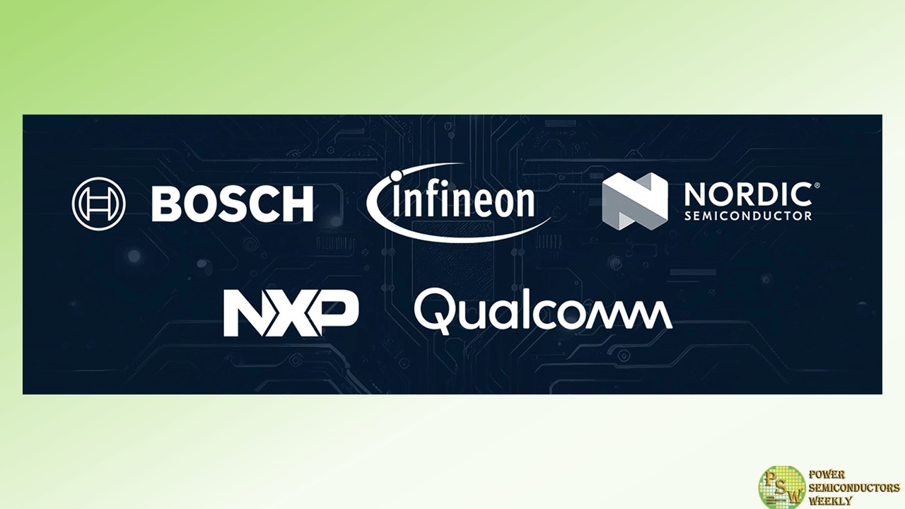
Semiconductor industry players Robert Bosch GmbH, Infineon Technologies AG, Nordic Semiconductor, NXP® Semiconductors, and Qualcomm Technologies, Inc., have come together to jointly invest in a company aimed at advancing the adoption of RISC-V globally by enabling next-generation hardware development.
Formed in Germany, this company will aim to accelerate the commercialization of future products based on the open-source RISC-V architecture. The company will be a single source to enable compatible RISC-V based products, provide reference architectures, and help establish solutions widely used in the industry. Initial application focus will be automotive, but with an eventual expansion to include mobile and IoT.
At its core, RISC-V encourages innovation, allowing any company to develop cutting-edge, customized hardware based on an open-source instruction set. Further adoption of the RISC-V technology will promote even more diversity in the electronics industry – reducing the barriers to entry for smaller and emergent companies and enabling increased scalability for established companies.
The company calls on industry associations, leaders, and governments, to join forces in support of this initiative which will help increase the resilience of the broader semiconductor ecosystem.
The company formation will be subject to regulatory approvals in various jurisdictions.
- Robert Bosch GmbH
“Bosch is convinced that initiatives promoting the RISC-V open specifications will bring the global mobility market a significant step further. The initiative now planned will greatly help to establish a reliable and efficient EU-based semiconductor ecosystem,” said Jens Fabrowsky, Executive Vice President at Bosch and responsible for the semiconductor business.
- Infineon Technologies AG
“As vehicles become software-defined and dependability requirements increase due to electrification and connectivity, for example, as well as through trends like autonomous driving, there is a general need for standardization and ecosystem compatibility across the industry, with CPUs being a key IP. We are proud to support the establishment of trusted RISC-V based automotive products with this initiative. The knowledge and expertise of leading market players will unleash the full potential of RISC-V in the automotive sector,” said Peter Schiefer, Division President of Infineon’s Automotive Division.
- Nordic Semiconductor
“Nordic Semiconductor is a committed and enthusiastic supporter of the RISC-V initiative and stands ready to drive the project forward. Nordic’s IoT solutions represent the leading edge of low power wireless technology and to retain that position it’s critical we maintain continuous access to efficient and powerful embedded microprocessors. An open collaboration with like-minded companies to continually enhance innovative RISC-V microprocessor IP and ensure a robust and reliable supply of the technology is the ideal answer to this challenge,” said Svein-Egil Nielsen, CTO/EVP R&D and Strategy, Nordic Semiconductor.
- NXP Semiconductors
“NXP is proud to be part of a new EU-based joint endeavor to pioneer fully certified RISC-V-based IP and architectures, initially for the automotive industry. The creation of a one-stop-shop ecosystem where customers can select turnkey assets will strengthen the adoption of RISC-V across many European industries,” said Lars Reger, Executive Vice President and Chief Technology Officer at NXP Semiconductors. “We thank the Artificial Intelligence Center Hamburg (ARIC) e.V. for their support of this collaboration.”
- Qualcomm Technologies, Inc.
“We are excited to come together with other industry players to drive the expansion of the RISC-V ecosystem through development of next-generation hardware. Qualcomm Technologies has been investing in RISC-V for more than five years and we’ve integrated RISC-V micro-controllers into many of our commercial platforms. We believe RISC-V’s open-source instruction set will increase innovation and has the potential to transform the industry,” Ziad Asghar, Senior Vice President of Product Management, Qualcomm Technologies, Inc.
Original – Infineon Technologies
-
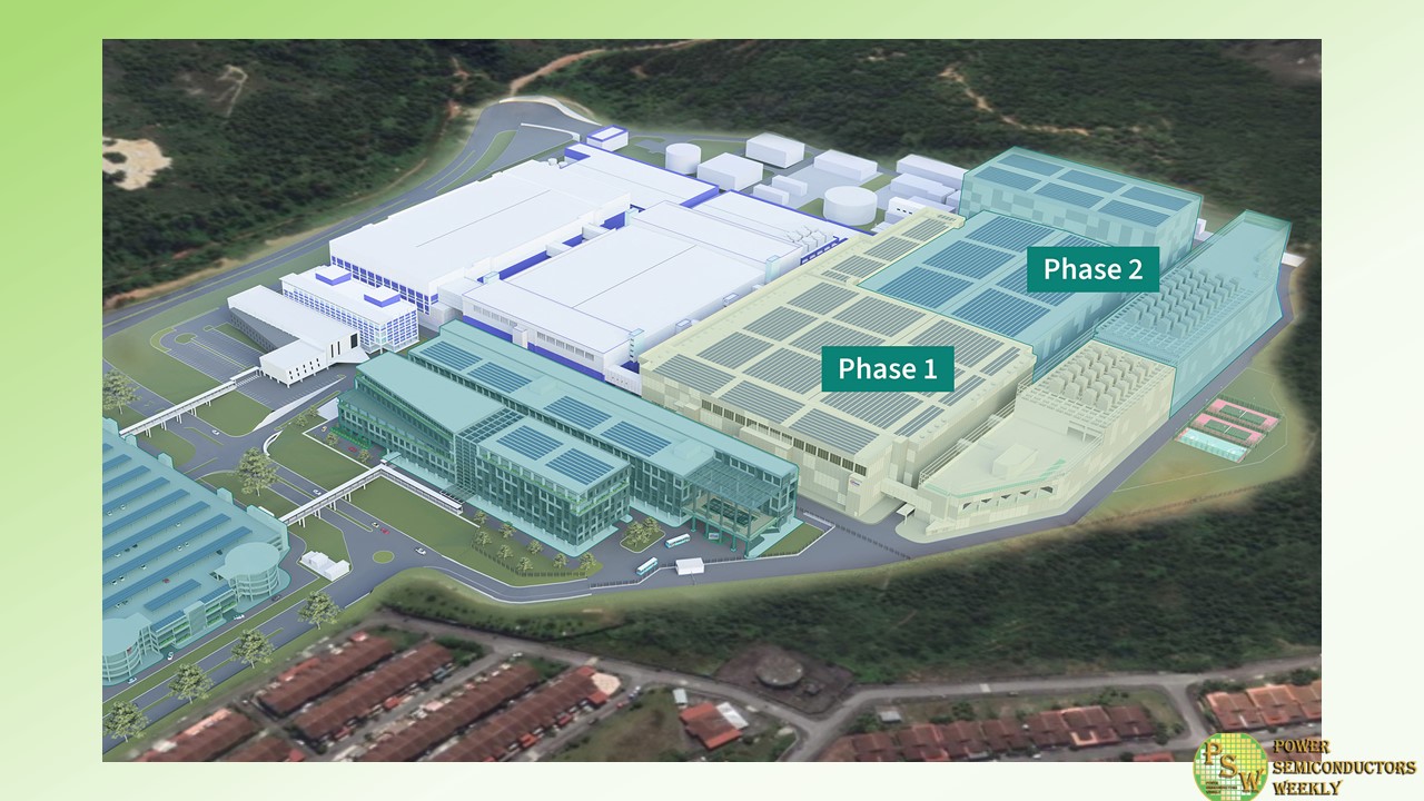
The decarbonization trend will result in strong market growth for power semiconductors, in particular those based on wide bandgap materials. As a leader in Power Systems, Infineon Technologies AG is now taking a further, decisive step to shape this market: By significantly expanding its Kulim fab – over and above the original investment announced in February 2022 – Infineon will build the world’s largest 200-millimeter SiC (silicon carbide) Power Fab. The planned expansion is backed by customer commitments covering about five billion euros of new design-wins in automotive and industrial applications as well as about one billion euros in pre-payments.
Over the next five years Infineon will additionally invest up to five billion euros in Kulim during a second construction phase for Module Three. The investment will lead to an annual SiC revenue potential of about seven billion euros by the end of the decade, together with the planned 200-millimeter SiC conversion of Villach and Kulim. This highly competitive manufacturing base will support Infineon’s SiC market share target of 30% towards the end of the decade. Infineon is confident that the company’s SiC revenue in the fiscal year 2025 will come in ahead of the target of one billion euros.
“The market for silicon carbide shows accelerating growth, not only in automotive but also in a broad range of industrial applications such as solar, energy storage and high-power EV charging. With the Kulim expansion, we will secure our leadership position in this market,” said Jochen Hanebeck, CEO of Infineon. “With the industry’s leading scale and a unique cost position, we are leveraging our competitive position of best-in-class SiC trench technology, the broadest package portfolio and unrivaled application understanding. These factors are the areas of differentiation and success in the industry.”
Infineon has been awarded new design wins of about five billion euros along with about one billion euros in prepayments from existing and new customers: In the automotive sector this includes six OEMs, three of them from China. Among the customers are Ford, SAIC and Chery. In the area of renewable energies customers include SolarEdge and three leading Chinese photovoltaic and energy storage systems companies.
In addition, Infineon and Schneider Electric agreed on a capacity reservation including prepayments for power products based on silicon and silicon carbide. Infineon and the respective customers will provide more details in separate announcements in the near future. The prepayments will contribute positively to Infineon’s cash flow in the coming years and shall be fully repaid in connection with the agreed sales volumes by 2030 at the latest.
The Right Honourable Dato’ Seri Anwar bin Ibrahim, Prime Minister of Malaysia, expressed his appreciation for Infineon’s commitment to creating a significant wide bandgap hub in the country. “Malaysia is putting in maximum efforts to meet its national target to decarbonize its economy and achieve net zero by 2050. Malaysia’s continued appeal as a preferred investment destination comes with a well-established landscape for developing innovative and sustainable technologies. In this vein, Infineon’s vision on green technology and sustainability puts it right at home in Malaysia.
Infineon and other well-established German corporations’ continued faith in Malaysia is a vote of confidence in Malaysia’s new economic growth agenda premised on inclusivity and sustainability, enabled by strong policies on knowledge transfer, quality investments, business enablement and socio-economic well-being based on equitable sharing of the nation’s wealth.”
The Minister of Investment, Trade and Industry (MITI), His Hon. Tengku Datuk Seri Utama Zafrul Aziz lauded Infineon’s expansion and said, “Infineon’s expansion of their world-class silicon carbide facility in Kulim marks a significant milestone in Malaysia’s pursuit of developing advanced manufacturing capabilities, creating high-skilled employment opportunities and positioning the country at the forefront of enabling green technologies, which are crucial to achieving our global sustainable development goals.
The innovative power semiconductor technologies manufactured in the SiC Power Fab will also bolster Malaysia’s position as a key player in the world’s semiconductor ecosystem, with a growing role specifically in the sustainable technology supply chain. I am heartened by Infineon’s sharing of Malaysia’s commitment to address the impact of climate change and I look forward to our long-term partnership for the further development of Malaysia’s green technologies ecosystem.”
Sustainability is a key element in the planning, construction and operation of the fab. The building is designed in a way that allows Infineon to make responsible use of resources such as electricity and water.
Original – Infineon Technologies
-
SiC power devices are changing and reshaping many industries today, providing numerous benefits over fundamental silicon-based semiconductors. One of the key advantages is a dramatically reduced power losses with increased efficiency achieved through silicon carbide exceptional material properties. SiC power semiconductors can operate at higher frequencies and temperatures delivering higher power densities and reduced cooling requirements. One of the industries benefiting much from the use of SiC power devices is the energy storage.
Adopting silicon carbide technology, energy storage systems can deliver great energy saving and much better overall system performance.
Reliability is one of the major requirements for any power electronics system, and ESS is no exception. That is why many ESS companies today choose SiC technology over Si. Silicon carbide power devices provide increased robustness and resistance when it comes to operating in extreme conditions. SiC temperature robustness allows to eliminate the risk of the system overheating – one of the major reasons for failure.
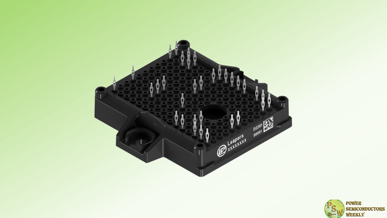
Leading the development process of SiC power devices for a variety of emerging applications including vehicle electrification, photovoltaics, and, of course, battery energy storage systems, Leapers Semiconductor is expanding its portfolio of the hybrid modules with the 3-level power module to provide increased reliability for the ESS, solar, and the other 3-level applications.
The all new DFH10AL12EZC1 power module integrates 1200V SiC MOSFET chips and 1200V IGBT chips in E2 package designed to correspond to high requirements set by the above-mentioned applications.
Leapers Semiconductor DFH10AL12EZC1 hybrid power module features:
- Blocking voltage:1200V
- Rds(on): 9.5mΩ (VGS =15V)/8.3mΩ (VGS =18V)
- Low Switching Losses
- High current density
- Press FIT Contact Technology
- 175°C maximum junction temperature
- Thermistor inside
DFH10AL12EZC1 hybrid power modules guarantee the enhanced efficiency, improved power conversion, and increased overall reliability and durability with reduced system size.
The other applications that will benefit from DFH10AL12EZC1 include:
- Solar inverter Systems
- Three-level Systems
- Energy Storage Systems
- High Frequency Switching Systems
Original – Leapers Semiconductor
-
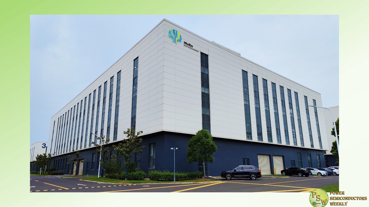
The opening ceremony of WeEnwin Jinshan Module Plant was held in the Shanghai Jinshan High-tech Industrial Development Zone. The ceremony marked the official commencement of WeEn’s world-first module plant, intended to produce various types of power module products utilized in consumer electronics, communications, new energy, and automotive applications. The products connect customers and the ecosystems, actively fostering the high-quality development of the industry.
Markus Mosen, WeEn Semiconductors Co., Ltd. CEO; Chen Song, COO; Tang Ziming, CFO; Wu Rui, CHRO; Peng Xijun, general manager of Shanghai New Jinshan Industrial Investment & Development Co., Ltd; Zhao Fei, deputy director of the Jinshan District Development and Reform Commission; Cao Qin, deputy director of the Jinshan District Investment Promotion Office; other relevant department heads of the New Jinshan Development Company; WeEn boards Zhang Xinyu, Chang Liang, and Zhu Fenglin; together with representatives from WeEn’s global partners, numerous customers, vendors, approximately 200 guests attended the event to personally witness this historic step in WeEn’s new journey.
Located in the Shanghai Bay Area High-tech Industrial and Development Zone, WeEn Jinshan Module Plant covers an area of 11,000 square meters. The construction of the plant began in August 2022. Eight months later in April 2023, the building quality and fire inspection compliance tests were successfully completed.
WeEn Semiconductors Co., Ltd. has invested approximately RMB 200 million in the wholly-owned new Jinshan Module Plant, which has introduced over a hundred of the industry’s most advanced power module production and testing equipment to meet the market’s mainstream demand for various types of module products.
It is worth underscoring that the newly established WeEnwin Module Plant has simultaneously set up an advanced packaging R&D center to develop and mass produce cutting-edge packaging technologies while researching the applicability of new materials.
To optimize efficiency and reliability, the fully automated module production line is equipped with top-notch processing capabilities, including lead-free chip bonding/silver sintering bonding, lead-free soldering/ultrasonic soldering of terminals, aluminum wire bonding, and copper tab connections. Currently, WeEnwin module plant. has obtained ISO9001 and IATF16949 certifications and undergone VDA6.3 process audits, evidence of the company’s robust system that guarantees top-quality products.
Peng Xijun, general manager of Shanghai New Jinshan Industrial Investment & Development Co., Ltd, warmly congratulated WeEnwin for the opening, noting that the event was a testimony of the concerted efforts of all parties. He further stated that the collective endeavors have significant importance in elevating the power semiconductor industry’s development level and accelerating the concentration of the optoelectronic chip industry in the high-tech industrial and development zone.
In addition, he expressed his wish for the high-tech zone, as it embarks on its new era journey, to continue harnessing resources and efforts and attracting policies aimed at strengthening the innovation chain, extending the industrial chain, and improving the ecosystem.
Meanwhile, Markus Mosen, WeEn Semiconductors Co., Ltd. CEO stated, “Given the favorable winds, this is the perfect time to set sail.” WeEn’s investment in the world’s first module factory has successfully transitioned from planning to operation according to schedule. Therefore, we remain grateful for the strong support from the Jinshan District People’s Government, Shanghai Bay Area High-tech Industrial Development Zone, and FITA Tech.
There is no doubt that without the collective efforts of our partners and team, this accomplishment would not have been possible. At WeEnwin, we will seize the opportunities of the era, leverage our product and technological strengths, and provide reliable and efficient power semiconductor devices to our customers and partners. As we inject new impetus into pragmatic cooperation, we remain confident in our ability to propel the ship of power device development toward a new journey.”
The operation of the WeEnwin Jinshan Module plant will enhance the efficiency of WeEn Semiconductors Co., Ltd.’s entire industry chain layout and services. In addition to producing the most advanced SCR / FRD / IGBT / SIC modules, the factory will significantly improve the experience of customers and partners by offering innovative modules and packaging services for the automotive and renewable energy markets. It is projected that the first batch of products from the new Jinshan Module Factory for Chinese and overseas customers will be shipped in the fourth quarter of 2023.
Original – WeEn Semiconductors
-
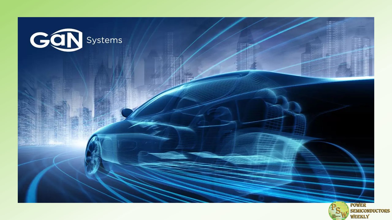
GaN Systems has partnered with ACEpower to expedite the widespread adoption of GaN technology in electric vehicles. By harnessing GaN Systems’ cutting-edge power semiconductors, extensive expertise in EV power electronics, and ACEpower’s exceptional track record in high-power system design and high-volume manufacturing capabilities, this partnership will accelerate the GaN-based electric vehicle power market in China.
GaN power semiconductors play a pivotal role in realizing the compact size, lightweight, and high efficiency demanded by the next generation of high-performance electric vehicles. By harnessing GaN Systems’ automotive-grade, high-performance GaN power transistors alongside ACEpower’s deep expertise in the power electronics industry, the companies are combining their distinctive capabilities to unlock the full potential of GaN performance advantages.
In addition to other areas, the partnership will focus on topology optimization and advanced integrated power modules, and high-frequency magnetics design to enhance crucial electric vehicle efficiency and power density significantly.
“We are delighted to announce our partnership with GaN Systems to accelerate GaN adoption in electric vehicles,” said Albert Wang, CEO of ACEpower. “Our longstanding relationship with GaN Systems, coupled with their unrivaled expertise in high reliability, automotive-qualified GaN semiconductors—a vital component for electric vehicles—brings great business opportunities in the fast growth Chinese EV market. Together, we are committed to driving innovation that will revolutionize electric vehicles, particularly in efficiency and power density, delivering substantial benefits to the industry.”
This combination tackles fundamental challenges related to traditionally larger, heavier, inefficient, and costlier power systems based on legacy silicon power transistors. GaN power transistors enable higher efficiency and power density at a faster switching speed for onboard chargers, DC/DC converters, and traction inverters. These advancements translate into faster charging, extended driving range, and reduced overall system costs.
“Today’s announcement marks a significant leap in our cooperative efforts with ACEpower to drive GaN adoption in the Chinese electric vehicle market,” said Jim Witham, CEO of GaN Systems. “This collaboration paves the way for disruptive and game-changing advancements in next-generation electric vehicles. Building upon our strong industry relationships with key players such as BMW, Toyota, and Vitesco, GaN Systems and ACEpower are poised to make a substantial impact in accelerating GaN adoption across the electric vehicle platform.”
GaN Systems and ACEpower’s shared vision extends to capturing substantial market value in emerging sectors such as data centers and electric vehicles. Future initiatives encompass the joint development of high-power density GaN-powered OBCs rated at 6.6kW and 11kW for electric vehicles, solidifying their commitment to driving innovation and advancing the power industry.
Original – GaN Systems
-
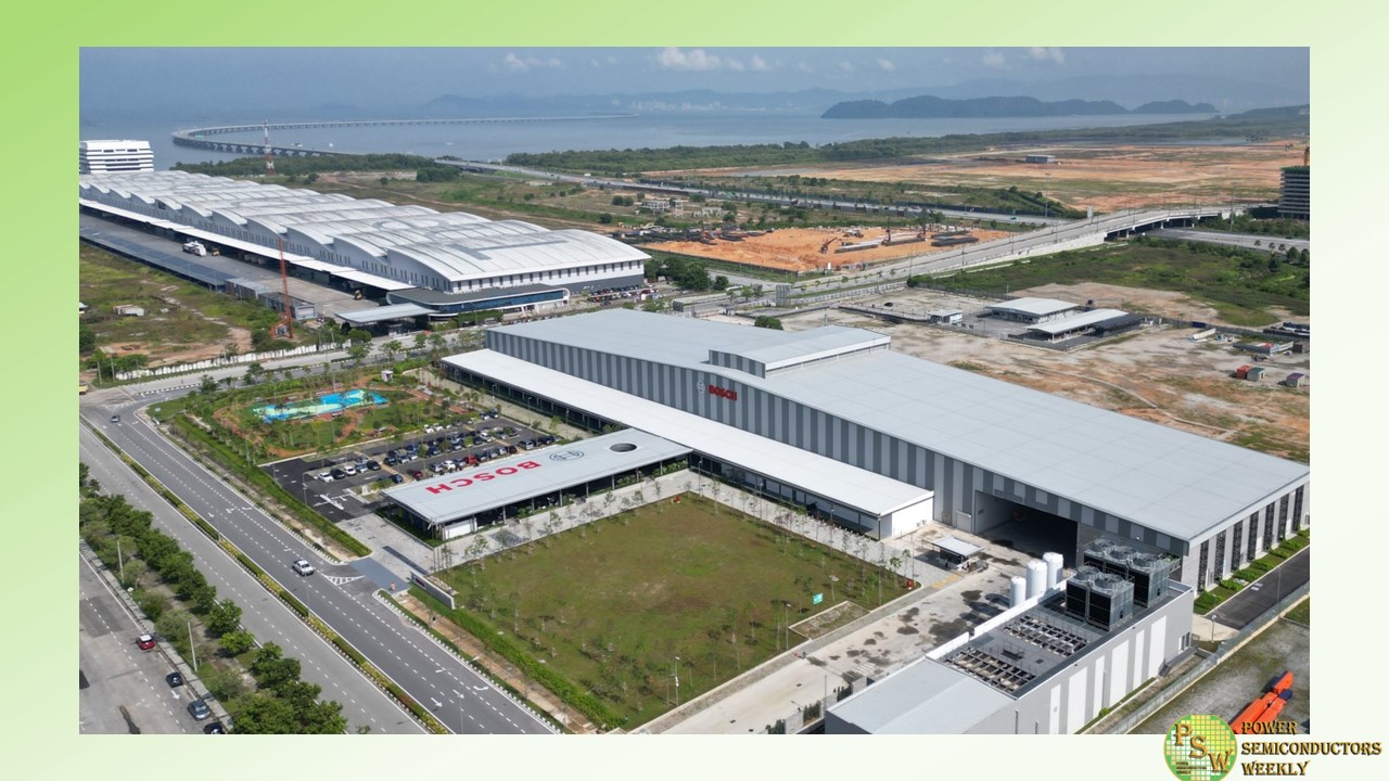
Global demand for chips for the automotive and consumer goods industries remains high. That is why Bosch is continuing to expand its semiconductor business. The company has now opened a new test center for chips and sensors in Penang, Malaysia, at a cost of some 65 million euros; it plans to invest a further 285 million euros at the site by the middle of the next decade.
“With our new semiconductor test center in Penang, we are creating additional capacity within our worldwide manufacturing network to meet the continued high demand for chips and sensors,” said Dr. Stefan Hartung, chairman of the Bosch board of management. “Semiconductors are a decisive success factor for all Bosch business areas, and the expansion of this business is strategically very important.”
In total, Bosch has some 100,000 square meters of land available on Penang’s mainland strip. The new test center currently covers more than 18,000 square meters and includes clean rooms, office space, and laboratories for quality assurance and manufacturing. By the middle of the next decade, up to 400 associates will be working there. With the new factory and a total of 4,200 associates, Penang is now Bosch’s biggest location in Southeast Asia.
Semiconductor manufacturing can basically be divided into two sections: frontend manufacturing and backend manufacturing. For the latter, Malaysia is an important hub in the global semiconductor supply chain. The country is estimated to cover around 13 percent of global backend manufacturing. According to official figures, in recent years the state of Penang has generated more than 5 percent of worldwide semiconductor revenue.
“The new test center in Penang brings our manufacturing network closer to the companies that serve the further value chain of semiconductor manufacturing as well as to customers in this important Asian market. That shortens delivery times and routes, and it improves our competitiveness,” says Dr. Markus Heyn, member of the Bosch board of management and chairman of the Mobility business sector.
The frontend is where the actual circuits are attached and patterned on the wafers; at Bosch, for example, this work is currently performed in the clean rooms of the wafer fabs in Reutlingen and Dresden. The backend is where the individual chips are then separated from the wafers, assembled, and tested. Bosch currently carries out most of the final testing of its semiconductors in Reutlingen, Germany; Suzhou, China; and Hatvan, Hungary.
Those locations will now be joined by the new test center in Penang, Malaysia. The fully connected plant is one of the most advanced semiconductor test centers in Southeast Asia. Here, Bosch will immediately begin testing semiconductors that the company manufactures at its frontend in Dresden, among other locations. “Our new test center in Penang completes our internal process chain, especially for semiconductors from Dresden,” Heyn says.
Bosch is pursuing a global growth strategy with its semiconductor business. Over the next three years, the company plans to invest some three billion euros in Dresden and Reutlingen, both as part of its own investment plan and under the auspices of the European IPCEI ME/CT (“Important Project of Common European Interest on Microelectronics and Communication Technologies”) funding program.
Following its expected acquisition of part of the business of TSI Semiconductors, based in Roseville, California, which is expected before the end of the year, Bosch plans to invest roughly an additional 1.4 billion euros in retooling the fab to support the latest manufacturing processes for silicon carbide semiconductors.
Original – Bosch
