-

Mitsubishi Electric Corporation announced that it has taken an equity position in Novel Crystal Technology, Inc., a Japanese company that develops and sells gallium-oxide wafers, a promising candidate for use in superior energy-saving power semiconductors that Mitsubishi Electric intends to develop at an accelerated pace in support of global decarbonization.
Novel Crystal Technology, one of the world’s first companies to develop, manufacture and sell gallium-oxide wafers for power semiconductors, and now a leading producer of these products, has manufacturing technology that Mitsubishi Electric will use in its production of gallium-oxide power semiconductors.
Mitsubishi Electric has been contributing to energy savings in power-electronic products by producing semiconductors made of silicon and silicon carbide (SiC). Recent advances have been achieved with SiC and gallium-nitride wafers, but gallium-oxide wafers are expected to help achieve even higher breakdown voltages and lower power dissipation.
Mitsubishi Electric now expects to accelerate its development of superior energy-saving gallium-oxide power semiconductors by combining its own expertise in the design and manufacture of low-energy-loss, highreliability power semiconductors with Novel Crystal Technology’s expertise in the production of gallium-oxide wafers.
Original – Mitsubishi Electric
-

Infineon Technologies AG and SolarEdge Technologies, Inc. announced the signing of a multi-year Capacity Reservation Agreement (CRA).
Extending the existing partnership, Infineon will supply SolarEdge with critical components for a variety of SolarEdge products. In addition to the CRA, the companies will collaborate on the development of future technologies and cutting-edge solar products based on wide-bandgap (WBG) materials that are key for global green energy supplies.
“We are excited to expand our strategic partnership with SolarEdge to shape innovation in green energy technologies and decarbonization”, said Andreas Urschitz, Chief Marketing Officer at Infineon. “Our long-lasting collaboration is an enormous asset for both companies that paves the way for breakthrough-innovation and accelerated growth, as we combine our expertise and resources. With the latest investments in silicon carbide (SiC) and gallium nitride (GaN) manufacturing capacity, Infineon underlines its commitment to be a leading partner in climate technologies such as solar power.”
Uri Bechor, Chief Operating Officer at SolarEdge, said: “Securing the capacity levels of critical components such as power and wide-bandgap from Infineon enhances SolarEdge’s supply chain resiliency. This Capacity Reservation Agreement with Infineon is in line with our strategy to continue leading the global industry in solar energy advancement.”
Original – Infineon Technologies
-
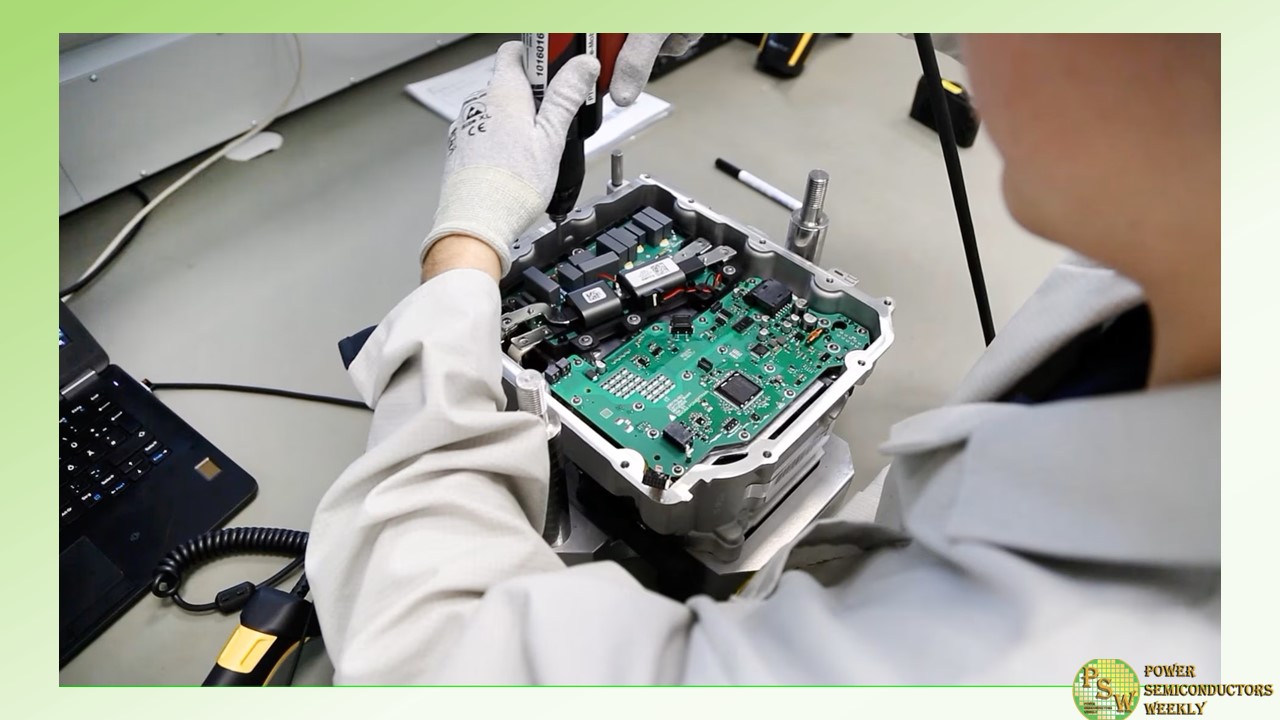
onsemi and Magna announced a long-term supply agreement (LTSA) for Magna to integrate onsemi’s EliteSiC intelligent power solutions into its eDrive systems.
By integrating onsemi’s industry-leading EliteSiC MOSFET technology, Magna eDrive systems can offer better cooling performance and faster acceleration and charging rates, improving efficiency and increasing the range of electric vehicles (EVs). Additionally, onsemi’s end-to-end silicon carbide (SiC) manufacturing capability, combined with its ability to ramp production quickly, improves Magna’s vertical integration and simplifies its supply chain to meet the growing demand for its SiC-based products for EVs.
“With range anxiety still a top deterrent to EV adoption, our technology enables Magna to go further, easing the transition to an electrified future,” said Asif Jakwani, senior vice president and general manager, Advanced Power Division, onsemi. “Our latest EliteSiC MOSFET technology enables increased power density and higher efficiency in traction inverters, resulting in improved gas-equivalent miles per gallon without compromising driving dynamics and safety.”
Simultaneous with the signing of the LTSA, the companies entered a separate agreement for Magna to also invest approximately $40 million for the procurement of new SiC equipment at onsemi’s New Hampshire and Czech Republic facilities to ensure access to future supply.
“We believe that a secure supply of silicon carbide chips will be critical to our ability to continue delivering innovative and efficient eDrive systems for our customers,” said Diba Ilunga, president Magna Powertrain. “Accordingly, we are both investing to grow SiC production capacity, and establishing the commercial basis for long-term supply of SiC-based chips to advance our electrification strategy and outpace the competition.”
Silicon carbide is a wide bandgap semiconductor substrate that is ideal for high-temperature, high-power applications such as electric vehicles, but it is incredibly difficult to produce. With a limited number of manufacturers and significant demand for SiC-based designs, OEMs and automotive suppliers are increasingly looking to secure long-term, reliable supply.
Original – onsemi
-
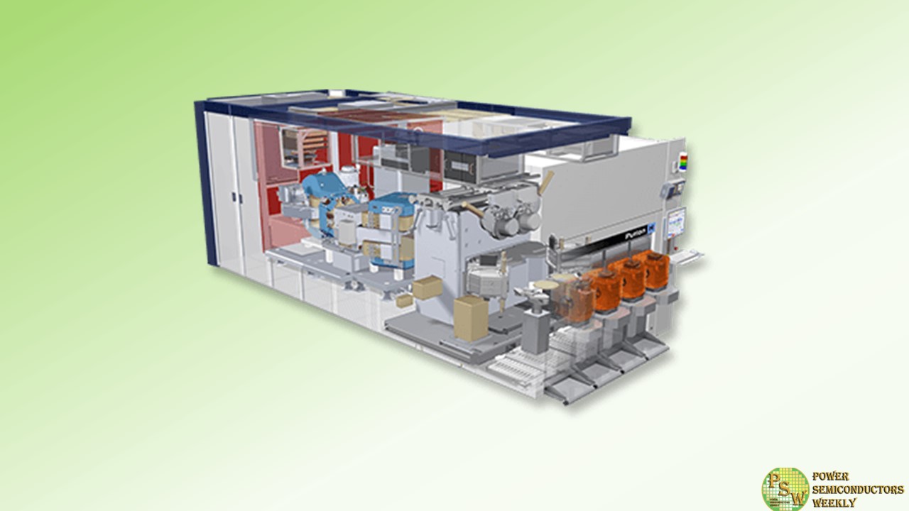
Axcelis Technologies, Inc. announced a shipment of a Purion H200™ SiC ion implant system to Wolfspeed. The evaluation system will be used to support the production of power devices for electric vehicle (EV) applications.
President and CEO Dr. Russell Low of Axcelis commented, “The power device market continues to grow rapidly and is a key driver of our growth globally. We are pleased to continue to support Wolfspeed’s fab capacity expansion and are also excited about the potential of this new opportunity focused on high current implant applications in silicon carbide power devices.”
“The popularity of electric vehicles is only steepening, and Wolfspeed is focused on scaling our capacity to meet the surge in demand for our silicon carbide devices. We partnered with Axcelis due to their expertise, highly differentiated features, and process control capabilities that are essential for power device applications,” said Missy Stigall, Wolfspeed senior vice president of global fab operations. “Together, we will work to ease supply chain constraints as more and more EVs utilizing Wolfspeed’s silicon carbide technology are introduced to the market.”
Wolfspeed is currently engaged in a $6.5 billion capacity expansion effort to dramatically increase production. This includes the John Palmour Manufacturing Center for Silicon Carbide, the world’s largest Silicon Carbide crystal growth facility currently under construction in North Carolina, and the final build-out of the company’s Mohawk Valley Fab in New York. Earlier this year the company also announced its plans to build a highly automated, cutting-edge 200mm wafer fabrication facility in Saarland, Germany.
Original – Axcelis Technologies
-

onsemi announced it has secured $1.95B in long-term supply agreements (LTSAs) for its intelligent power technologies with leading global manufacturers of solar inverters, contributing to onsemi’s position as the number one power semiconductor supplier in this rapidly growing market.
By offering superior die technology with optimized and customized module design and packaging, onsemi enables solar inverter providers to compete on time-to-market, product development, supply resilience and robust quality assurance. With these benefits, the company has signed LTSAs with eight of the top 10 solar inverter suppliers, emphasizing the reputation onsemi has earned as a trusted industry partner.
“Solar power has emerged as one of the fastest growing markets and offers the most cost-competitive source for large-scale renewable energy installations,” said Asif Jakwani senior vice president and general manager, Advanced Power Division, Power Solutions Group, onsemi. “With onsemi’s intelligent power technologies, customers can achieve greater efficiency and power density to capture and save as much energy from the sun as possible to advance our common mission towards a more sustainable future.”
Solar inverters convert Direct Current (DC) electricity generated by solar panels to grid-compatible Alternating Current (AC). In the conversion process, some energy is lost as heat. onsemi’s technology enables solar inverters – ranging from utility to residential – applications to be smaller, lighter, and more efficient, which minimizes energy loss and can reduce the overall system cost.
Original – onsemi
-
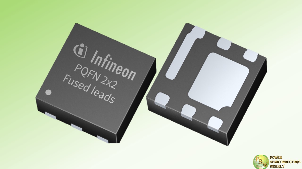
A small footprint of discrete power MOSFETs plays a critical role in achieving space savings, cost reduction, and easy-to-design applications. Additionally, higher power density can lead to layout routing flexibility and overall system size reduction. By expanding the current PQFN 2×2 portfolio with the new best-in-class OptiMOS™ power MOSFETs, Infineon Technologies AG offers benchmark solutions optimized for efficiency and performance in a small footprint. The new products are ideal for applications like synchronous rectification in switched mode power supplies (SMPS) for servers, telecom, and portable- and wireless chargers. Additional applications also include electric speed controllers for small brushless motors in drones.
The new OptiMOS 6 40 V and OptiMOS 5 25 V and 30 V power MOSFETs further optimize the proven OptiMOS technology for high-performance designs. They offer leading-edge silicon technology, package reliability, and superior thermal resistance (R thJC, max = 3.2 K/W) in the ultra-small PQFN 2×2 mm² package. The new devices combine industry-leading low on-resistance R DS(on) with industry-leading figures of merit (FOMs, Q G and Q OSS) for outstanding dynamic switching performance. As a result, MOSFETs with ultra-low switching and reduced conduction losses ensure optimal energy efficiency and power density, all while simplifying thermal management.
With the compact PQFN 2×2 mm² package outline, the OptiMOS power switches enable an improved system form factor with smaller, more flexible geometric outlines for end-user applications. The MOSFETs facilitate reliable system design with less need for paralleling, significantly reducing space and system cost.
Original – Infineon Technologies
-

Qorvo® announced the release of QSPICE™, a new generation of circuit simulation software that provides power and analog designers significantly higher levels of design productivity through improved simulation speed, functionality and reliability.
In addition to advancing the state of the art in analog simulation technology, QSPICE allows designers to simulate complex digital circuits and algorithms. Its unique combination of modern schematic capture and fast mixed-mode simulation make it the ideal tool to solve the increasingly complex hardware and software challenges faced by today’s system designers.
“QSPICE enables an entirely new generation of mixed-mode circuit simulation,” said Jeff Strang, general manager for Qorvo’s Power Management business. “In the past, power designers relied on analog circuits and silicon power switches. Today, digital control and compound semiconductors are common elements of advanced power designs. Whether an engineer is developing AI algorithms for EV battery charging, optimizing a Qorvo pulsed-radar power supply or evaluating the newest silicon carbide FETs, QSPICE is the perfect platform for innovation.”
Qorvo’s QSPICE is available free of charge and offers numerous enhancements over legacy analog modeling tools. These improvements include:
- Complete support for advanced analog and digital system simulations, such as those used in AI and machine-learning applications.
- An upgraded simulation engine that uses advanced numerical methods and is optimized for modern computing hardware, including a GPU-rendered user interface and SSD-aware memory management, to provide dramatically higher speed and accuracy.
- Reduced overall runtimes and a 100% completion rate, based on Qorvo benchmark tests with a suite of challenging test circuits. This compares to a failure rate of up to 15% with these same test circuits using other popular SPICE simulators.
- Availability of a regularly updated QSPICE model library featuring Qorvo’s silicon carbide and advanced power management solutions, making it easy for customers to evaluate and design with Qorvo power.
QSPICE is available now at www.qspice.com and is actively supported by Qorvo as well as a robust user community through Qorvo’s QSPICE forum at forum.qorvo.com.
Original – Qorvo®
-

Wide Bandgap (WBG) semiconductors play a strategic role in driving innovation and creating energy efficient and high-performance electronics. Demand for these semiconductors is fueled by sustainability, industry advancements, and advanced connectivity.
However, meeting this demand requires addressing challenges like cost, technology reliability, and geo-politic chaos among others. While the global WBG semiconductor industry is poised for unprecedented growth in the next 10 years, it would be critical to prioritize the opportunities, and effectively tackle the challenges to meet the short-term and long-term demands.
Join Frost & Sullivan for an engaging and thought-provoking Think Tank on “WBG Semiconductors: Overcoming Challenges, Unlocking Potential” on July 28, at 10:00 AM, EDT. The distinguished panel of semiconductor professionals will share their expertise and experiences and will address pressing questions like:
- How can WBG semiconductors play a central role in driving sustainability goals?
- How can WBG semiconductors contribute to improving efficiency in renewable energy systems and energy infrastructure?
- What role would regulations and standards play in driving the adoption of WBG semiconductors?
- Electric vehicles (EVs) have long been strong advocates for WBG semiconductors – What are the current opportunities beyond EV that demand immediate action?
Mark your calendars to engage in discussion with:
- Prabhu Karunakaran, Industry Principal at Frost & Sullivan
- Jonathan Robinson, VP Research, Power and Energy at Frost & Sullivan
- Stephen Oliver, Marketing & Investor Relations at Navitas Semiconductor
- Alexey Cherkasov, Marketing & Sales Director at Leapers Semiconductor
Original – Frost & Sullivan
-
The European Commission has approved the “Important Project of Common European Interest on Microelectronics and Communication Technologies” (IPCEI-ME/CT) with the aim of initiating complex and investment-intensive projects that could not otherwise be realized. This involves 68 projects from 14 member states – and two of those comes from Semikron Danfoss.
Semikron Danfoss is planning the further development of diodes based on thin-wafer technology and the development of a new edge structure – as well as the establishment of automotive module production based on Direct Press Die technology in Nuremberg, a continuation of the activities from the IPCEI on Microelectronics project. And in Slovakia, development activities and an expansion of production for industrial modules are planned.
Projects funded under the IPCEI -ME/CT will enable the development of new technologies and products that will make a decisive contribution to the further reduction of CO2 emissions and will secure growth and jobs in Europe. The Semikron Danfoss projects address the objectives of the European Union to strengthen competitiveness and security of supply in key technologies for both the digital and the green transformation process.
Power semiconductors are an important multiplier along the value chain of many products. The projects also aim to expand European cooperation with universities and research institutes as well as suppliers. The member states are now starting the implementation process and will determine the requirements of the projects based on the EU decision. Thanks to the prior approval of the early start of the initiatives, the projects have already been launched. The official funding commitment from the federal government and the state of Bavaria is expected shortly for Germany.
Original – Semikron Danfoss
-
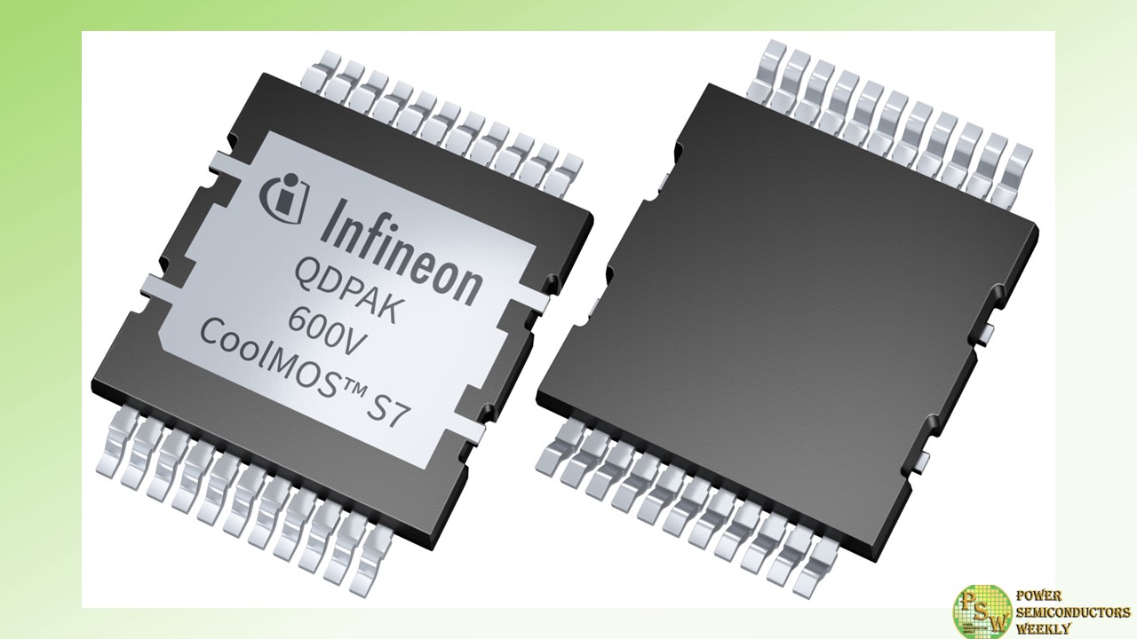
In static switching applications, power designs focus on minimizing conduction losses, optimizing thermal behavior, and achieving compact and lightweight systems while ensuring high quality at a low cost. To meet the needs of next-generation solutions, Infineon Technologies AG is expanding its CoolMOS™ S7 family of high-voltage superjunction (SJ) MOSFETs.
The devices are aiming at SMPS, solar energy systems, battery protection, solid-state relays (SSR), motor-starters and solid-state circuit breakers, as well as PLCs, lighting control, HV eFuse/eDisconnect, (H)EV on-board chargers.
The portfolio extension includes innovative QDPAK top-side cooling (TSC) packages and offers a wide range of features in a small footprint. This makes it highly advantageous for low-frequency switching applications while optimizing cost positioning.
Thanks to the novel high-power QDPAK packaging, they offer an R DS(on) of only 10 mΩ, which is the lowest on the market in this voltage class and the lowest in SMD packages. By minimizing conduction losses of the MOSFETs, the CoolMOS S7/S7A solutions contribute to higher overall efficiency and provide an easy and cost-optimized way to improve system performance.
The CoolMOS S7 power switches also effectively manage heat dissipation with improved thermal resistance. Thanks to the innovative and efficient QDPAK packaging, they also reduce or even eliminate the need for heat sinks in solid-state designs, resulting in more compact and lighter systems.
The MOSFETs are available in both top-side and bottom-side variants, and feature high-pulse current capability, enabling them to handle sudden surges of current. In addition, they exhibit body diode robustness to ensure reliable operation during AC line commutation.
With fewer components required, they reduce part count, resulting in flexible system integration, lower BOM costs, and total cost of ownership (TCO). In addition, these MOSFETs enable shorter reaction times, particularly when breaking a current, facilitating smoother and more efficient operation.
Original – Infineon Technologies
