-
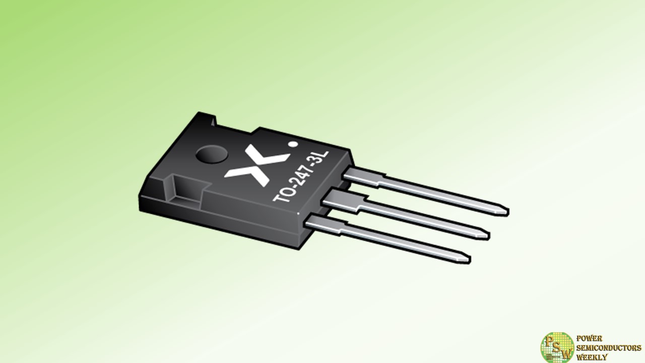
Nexperia launched its entry to the insulated gate bipolar transistor (IGBT) market with a range of 600 V devices, starting with the 30A NGW30T60M3DF. By adding IGBTs to its extensive portfolio, Nexperia is addressing the growing demand for efficient, high-voltage switching devices with a range of performance and cost requirements.
These enable higher power density in power conversion and motor drive applications, including industrial motor drives like servo motors ranging from 5 to 20 kW (20 kHz), robotics, elevators, operating grippers, in-line manufacturing, power inverters, uninterruptible power supply (UPS), photovoltaic (PV) strings, EV-charging, and induction heating and welding.
IGBT is a relatively mature technology. Nonetheless, the market for these devices is expected to grow in line with the increased adoption of solar panels and electric vehicle (EV) chargers. Nexperia’s 600 V IGBTs feature a robust, cost-effective carrier-stored trench-gate advanced field-stop (FS) construction, providing exceptionally low conduction and switching loss performance with high levels of ruggedness in operating temperatures up to 175°C. This improves the efficiency and reliability of power inverters, induction heaters, welding equipment and industrial applications like motor drives and servos, robotics, elevators, operating grippers, and in-line manufacturing.
Designers can choose between the medium speed (M3) and high speed (H3) series IGBTs. These IGBTs have been designed with very tight parameter distributions, allowing multiple devices to connect safely in parallel. In addition, lower thermal resistance than competing devices enables them to provide higher output power. These IGBTs are also fully rated as soft fast reverse-recovery diodes. This means they are suitable for rectifier and bi-directional circuit applications or to protect against overcurrent conditions.
“With the release of these IGBTs, Nexperia provides designers with a greater choice of power-switching devices for a broad range of power applications”, according to Dr. Ke Jiang, General Manager Business Group Insulated-Gate Bipolar Transistors & Modules at Nexperia. “IGBTs are the ideal complement to Nexperia’s existing range of CMOS and wide-bandgap switching devices, making Nexperia a one-stop-shop for power electronics designers.”
These IGBTs are available in a standard, lead-free, TO247-3L package and are HV-H3TRB qualified for outdoor applications. Nexperia plans to follow this release with a series of 1200 V IGBTs. To learn more about Nexperia’s IGBTs, visit: https://www.nexperia.com/igbts
Original – Nexperia
-

Navitas Semiconductor has confirmed continued supply of leading-edge gallium nitride (GaN) power ICs. On July 3rd, 2023, China’s Ministry of Commerce announced it would put in place certain restrictions on the exporting of gallium and germanium, among other materials, starting in August. Navitas’ wafer technology is ‘GaN-on-Si’. The wafer subcontract manufacturer has verified that their production remains unaffected by the export restrictions, given multiple sources of gallium world-wide.
As a result, Navitas does not expect customer deliveries to be impacted or its business to be adversely affected by the export restrictions.
Significant sources of gallium are available worldwide, as it is a natural by-product in the production of other metals such as aluminum. Navitas does not use germanium in any product.
Original – Navitas Semiconductor
-
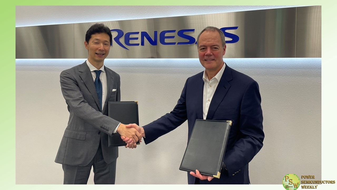
Renesas Electronics Corporation and Wolfspeed, Inc. announced the execution of a wafer supply agreement and $2 billion (USD) deposit by Renesas to secure a 10 year supply commitment of silicon carbide bare and epitaxial wafers from Wolfspeed. The supply of high-quality silicon carbide wafers from Wolfspeed will pave the way for Renesas to scale production of silicon carbide power semiconductors starting in 2025. The signing ceremony of the agreement was held at Renesas’ headquarters in Tokyo between Hidetoshi Shibata, President and CEO of Renesas, and Gregg Lowe, President and CEO of Wolfspeed.
The decade-long supply agreement calls for Wolfspeed to provide Renesas with 150mm silicon carbide bare and epitaxial wafers scaling in CY2025, reinforcing the companies’ vision for an industry-wide transition from silicon to silicon carbide semiconductor power devices. The agreement also anticipates supplying Renesas with 200mm silicon carbide bare and epitaxial wafers after the recently announced John Palmour Manufacturing Center for Silicon Carbide (the “JP”) is fully operational.
The need for more efficient power semiconductors, which supply and manage electricity, is dramatically increasing throughout automotive and industrial applications, spurred by the growth of electric vehicles (EVs) and renewable energy. Renesas is moving quickly to address the growing demand for power semiconductors by expanding its in-house manufacturing capacity. The company recently announced the restart of its Kofu Factory to produce IGBTs, and establishment of a silicon carbide production line at its Takasaki Factory.
Compared to conventional silicon power semiconductors, silicon carbide devices enable higher energy efficiency, greater power density and a lower system cost. In an increasingly energy-conscious world, the adoption of silicon carbide is becoming ever more pervasive across multiple high-volume applications spanning EVs, renewable energy and storage, charging infrastructure, industrial power supplies, traction and variable speed drives.
“The wafer supply agreement with Wolfspeed will provide Renesas with a stable, long-term supply base of high-quality silicon carbide wafers. This empowers Renesas to scale our power semiconductor offerings to better serve customers’ vast array of applications,” said Hidetoshi Shibata, President and CEO of Renesas. “We are now poised to elevate ourselves as a key player in the accelerating silicon carbide market.”
“With the steepening demand for silicon carbide across the automotive, industrial and energy sectors, it’s critically important we have best-in-class power semiconductor customers like Renesas to help lead the global transition from silicon to silicon carbide,” said Gregg Lowe, President and CEO of Wolfspeed. “For more than 35 years, Wolfspeed has focused on producing silicon carbide wafers and high-quality power devices, and this relationship marks an important step in our mission to save the world energy.”
The Renesas $2 billion deposit will help support Wolfspeed’s ongoing capacity construction projects including the JP, the world’s largest silicon carbide materials factory in Chatham County, North Carolina. The state-of-the-art, multi-billion-dollar facility is targeted to generate a more than 10-fold increase from Wolfspeed’s current silicon carbide production capacity on its Durham, North Carolina campus. The facility will produce primarily 200mm silicon carbide wafers, which are 1.7x larger than 150mm wafers, translating into more chips per wafer and ultimately, lower device costs.
Original – Renesas Electronics
-

Microchip Technology Incorporated announced a multi-year initiative to invest approximately $300 million in expanding its operations in India, one of the world’s fastest-growing semiconductor industry hubs.
“Microchip is making a significant strategic commitment to growing our operations in India, whose meteoric growth has established it as one of the top sources of business and technical resources in our sector,” said Ganesh Moorthy, President and CEO of Microchip. “Our investments here will enable us to both benefit from and contribute to the country’s increasingly important role in the global semiconductor industry.”
Microchip’s planned investments are focused on:
- Additional improvements to Microchip’s Bangalore and Chennai facilities and the new research and development center in Hyderabad that the company inaugurated in a ceremony today
- Expanding and enhancing its engineering labs
- Serving the technical and business support requirements of a large and growing set of customers in India
- Accelerating hiring as the company taps into India’s growing talent pool
- Sponsoring technical consortia and supporting academic institutions and programs
- Launching a variety of Corporate Social Responsibility (CSR) programs tailored to regional needs
Approximately 2,500 Microchip employees in India are integral to the company’s semiconductor design and development, sales and support, IT infrastructure and application engineering operations. They strengthen corporate initiatives, support 2,000 customers in the region and make valuable contributions across more than 25 business units that develop solutions for industrial, automotive, data center, aerospace and defense, communications and consumer industries.
“Microchip’s investments in India over nearly two and a half decades have augmented its headcount growth, resulting in building a center of excellence for engineering deliverables and solutions for Microchip’s global success,” said Krishna Moorthy, President and CEO of the India Electronics and Semiconductor Association (IESA). “We look forward to celebrating Microchip’s continued progress in India as it embarks on this impressive growth campaign.”
IESA and Counterpoint Research recently reported that India’s semiconductor market is expected to reach $64 billion USD by 2026, which is nearly triple its 2019 size of $22.7 billion USD. The Semiconductor Industry Association wrote in its February 2023 India Semiconductor Sector white paper that the country now accounts for 20 percent of the total global design workforce. Together, IESA and SIA announced in January 2023 their plans to jointly build on what India has already accomplished as a major hub for semiconductor research, chip design and equipment engineering, with the goal of unlocking even greater future potential.
Original – Microchip Technology
-

Navitas Semiconductor and Plexim GmbH announced a partnership to release GeneSiC G3™ SiC MOSFET and Gen 5 MPS diode PLECS thermal loss models for highly-accurate simulations of complete power electronics systems.
Power designers can simulate power and thermal losses in various soft- and hard-switching applications. Proprietary GeneSiC trench-assisted planar-gate MOSFET technology delivers the lowest RDS(ON) at high temperature and the highest efficiency at high speeds, and new MPS diodes with ‘low-knee’ characteristics drive unprecedented, industry-leading levels of performance, robustness and quality.
“Accurate, empirically-based simulation models maximize the chance of first-time-accurate designs, accelerating time-to-market and time-to-revenue,” noted Dr. Ranbir Singh, Navitas EVP for the GeneSiC business line. “For the power designer, understanding the leading-edge performance of GeneSiC MOSFETs and MPS diodes with detailed device characteristics, plus power, efficiency and thermal analysis is a critical competitive advantage.”
“The intuitive and highly-efficient PLECS lookup-table based approach to simulating thermal semiconductor losses in complex power electronic circuits is key,” said Kristofer Eberle, Plexim, North America. “Unlike legacy modeling approaches that are not well-suited to new wide bandgap materials, PLECS uses a simplified, but accurate behavioral description to highlight the superior performance of the GeneSiC MOSFETs.”
PLECS models for GeneSiC MOSFETs and MPS diodes are available via genesicsemi.com.
Original – Navitas Semiconductor
-

Elmos Semiconductor SE, one of the world’s leading suppliers of mixed-signal automotive semiconductors, and Littelfuse, Inc., USA, entered into a definitive agreement on the sale of the Elmos wafer fab at the Dortmund site to Littelfuse. Elmos has agreed to sell the wafer fab at a net purchase price of approximately 93 million Euro. Under the agreement, Littelfuse will acquire the Dortmund wafer fab with a highly skilled technology team of approximately 225 employees. All other activities, including testing operations, will remain with Elmos.
In acquiring the Dortmund wafer fab, Littelfuse enhances its capabilities in power semiconductors for high-growth power conversion applications like renewables, energy storage, and e-Mobility charging infrastructure.
“Today’s agreement is a milestone for semiconductor production in Dortmund and it will strengthen Germany’s standing as a high-tech location. As a fabless company, Elmos will make even greater use of advanced technologies to deliver groundbreaking innovations in mixed-signal semiconductors. Elmos is already the global market leader for certain applications in the automotive industry. We want to use this strong position to shape our future growth,” says Dr. Arne Schneider, CEO of Elmos Semiconductor SE.
Headquartered in Chicago, Illinois, United States, Littelfuse, Inc. is a diversified, industrial technology manufacturing company empowering a sustainable, connected and safer world. The company operates across more than 20 countries, and with approximately 18,000 global associates. Its products are found in a variety of industrial, transportation and electronics end markets. In Germany, Littelfuse operates various manufacturing, sales and R&D sites.
The closing of the transaction is expected to be effective December 31, 2024, and is subject to certain closing conditions and regulatory approvals, among them the investment control procedure under foreign trade law conducted by the German Federal Ministry for Economic Affairs and Climate Action. Elmos will retain full operational control over the wafer fab until the closing date.
In addition, Elmos and Littelfuse have agreed to enter into a defined multi-year capacity sharing arrangement with an initial term lasting through 2029, with Elmos buying defined volumes of wafers produced at the fab. This long-term agreement supplements the existing supply arrangements with Elmos’ other foundry partners and ensures that Elmos has the necessary capacities to meet projected customer demand.
“This is good news for the Elmos wafer fab team. We are delighted for Littelfuse to further develop the wafer fab in Dortmund for power semiconductors. Our employees are now expecting a quick review procedure by the relevant authorities,” says Dr. Schneider.
Following regulatory approvals of the transaction, the buyer will make a payment of approximately 37 million Euro. The remainder of the purchase price will be paid at closing. The transaction has no major effects on EBIT in fiscal year 2023, which is why the current forecast for the full-year EBIT margin in 2023 (25% ± 2 percentage points) continues to apply.
Cash flow is expected to be positively influenced in fiscal year 2023 by the payment of approximately 37 million Euro after regulatory approvals. Irrespective of the transaction, Elmos continues to increase its efforts to expand testing capacities for future growth. The company now anticipates capital expenditures of approximately 19% ± 2 percentage points of sales in fiscal year 2023 (previously: 17% ± 2 percentage points). As a result, Elmos now expects a negative operating adjusted free cash flow in 2023.
Original – Elmos Semiconductor
-
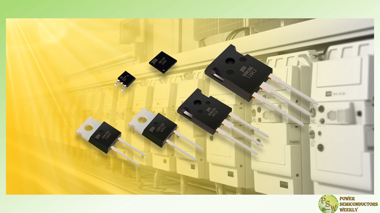
Bourns, Inc. announced its first 650 V – 1200 V Silicon Carbide (SiC) Schottky Barrier Diodes (SBDs). The Bourns® SiC SBD line consists of six models engineered to provide excellent current carrying and thermal capabilities and high power density for increased performance and reliability. These capabilities make Bourns® SiC SBDs optimal high efficiency power conversion solutions for the growing variety of high frequency applications that need to meet reduced size and lower system cost requirements.
Telecom/Server Switched-Mode Power Supplies (SMPS), photovoltaic inverters, PC power and motor drives are a few of the applications that can benefit from the features provided in the Bourns® BSD Series SiC SBDs.
To address ongoing design demands for ever higher power efficiency, Bourns® SiC SBDs feature low forward voltage (VF) and high thermal conductivity, which increases efficiency while lowering power dissipation, satisfying application requirements of 650 V and 1200 V solutions.
The series also has no reverse recovery current to reduce EMI, enabling these SiC SBDs to significantly lower energy losses. In addition to offering 650 V to 1200 V operation with currents in the 6-10 A range, the six new BSD models of wide band gap diodes from Bourns offer designers various forward voltage, current and package options including TO220-2, TO247-3, TO252, and DFN8x8.
The six Bourns® Model BSD SiC SBDs are available now. These models are RoHS compliant, halogen free, Pb free and their epoxy potting compound is flame retardant to the UL 94V-0 standard.
For more detailed product information, please see: www.bourns.com/products/diodes/silicon-carbide-sic-schottky-barrier-diodes
Original – Bourns
-
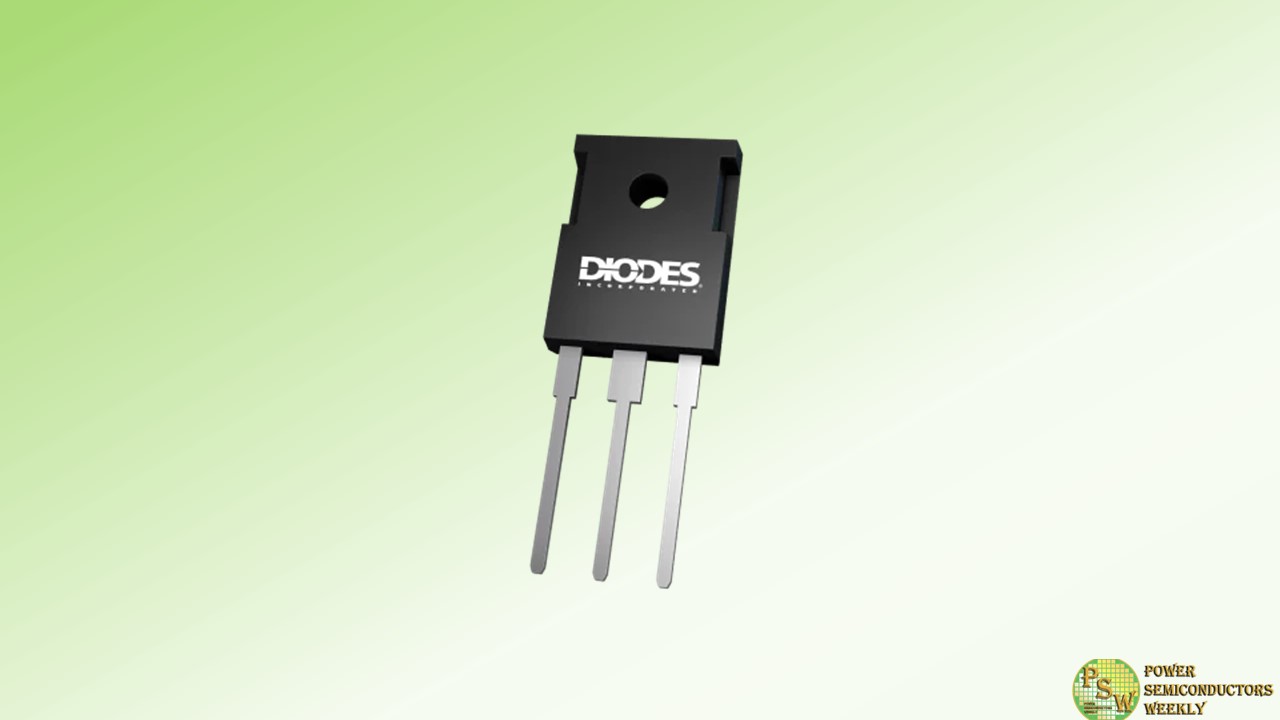
Diodes Incorporated announced a further enhancement of its wide-bandgap product offering with the release of the DMWSH120H90SM4Q and DMWSH120H28SM4Q automotive-compliant Silicon Carbide (SiC) MOSFETs. These N-channel MOSFETs respond to the increasing market demand for SiC solutions that enable better efficiency and higher power density in electric and hybrid-electric vehicle (EV/HEV) automotive subsystems like battery chargers, on-board chargers (OBC), high-efficiency DC-DC converters, motor drivers, and traction inverters.
The DMWSH120H90SM4Q operates safely and reliably up to 1200VDS with a gate-source voltage (Vgs) of +15/-4V and has an RDS(ON) of 75mΩ (typical) at 15Vgs. This device is designed for OBCs, automotive motor drivers, DC-DC converters in EV/HEV, and battery charging systems.
The DMWSH120H28SM4Q operates at up to 1200VDS, +15/-4Vgs, and has a lower RDS(ON) of 20 mΩ (typical) at 15Vgs. This MOSFET has been designed for motor drivers, EV traction inverters, and DC-DC converters in other EV/HEV subsystems. Low RDS(ON) enables these MOSFETs to run cooler in applications that require high power density.
Both products have low thermal conductivity (RθJC=0.6°C/W), enabling drain currents up to 40A in the DMWSH120H90SM4Q and 100A in the DMWSH120H28SM4Q. They also have fast intrinsic and robust body diodes with low reverse recovery charge (Qrr) of 108.52nC in the DMWSH120H90SM4Q and 317.93nC in the DMWSH120H28SM4Q. This enables them to perform fast switching with reduced power losses.
By using the planar manufacturing process, Diodes has created new MOSFETs that offer more robust and reliable performance in automotive applications—and with increased drain current, breakdown voltage, junction temperature, and power rings as compared to previously released versions. The devices are available in a TO247-4 (Type WH) package, which offers an additional Kelvin sense pin. This can be connected to the source to optimize switching performance, enabling even higher power densities.
Original – Diodes Incorporated
-
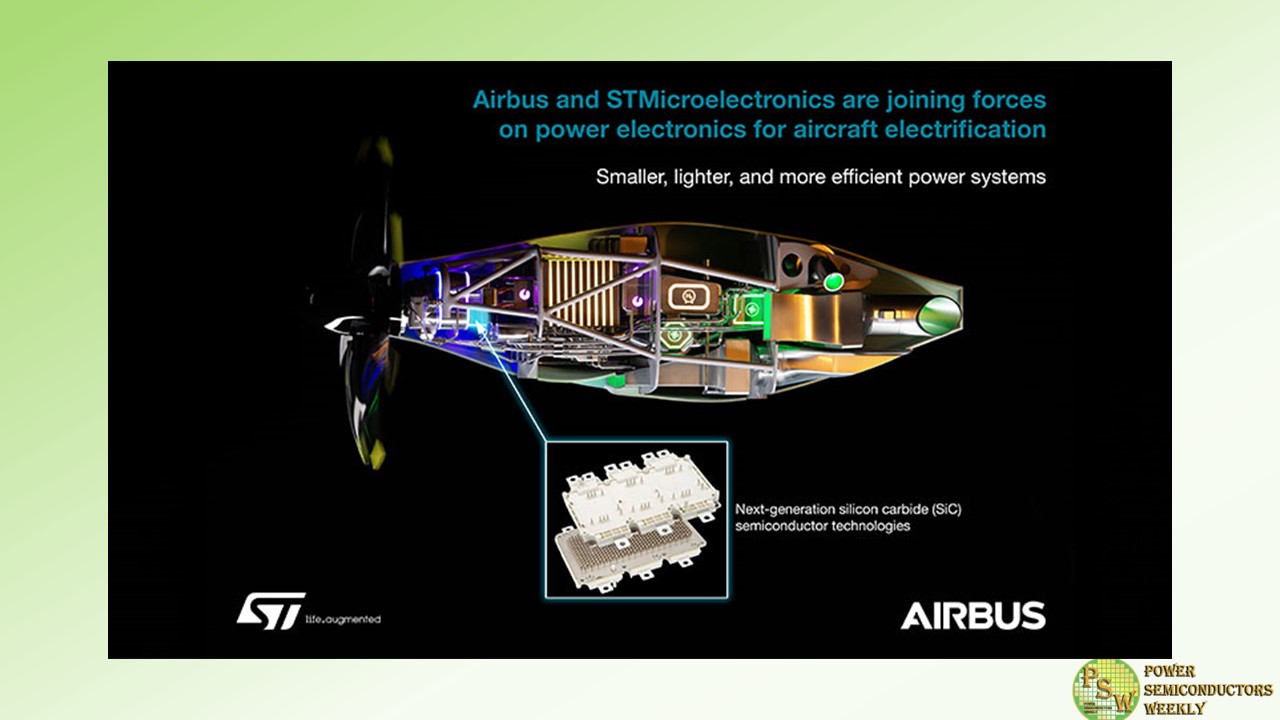
Airbus, a global pioneer in the aerospace industry, and STMicroelectronics, have signed an agreement to cooperate on power electronics Research & Development to support more efficient and lighter power electronics, essential for future hybrid-powered aircraft and full-electric urban air vehicles.
The collaboration builds on evaluations already conducted by both companies to explore the benefits of wide bandgap semiconductor materials for aircraft electrification. Wide bandgap semiconductors like Silicon Carbide (SiC) and Gallium Nitride (GaN) have superior electrical properties compared with traditional semiconductors like silicon. They enable the development of smaller, lighter and more efficient high-performance electronic devices and systems, particularly in applications requiring high power, high frequency, or high-temperature operations.
The cooperation will focus on developing SiC and GaN devices, packages, and modules adapted for Airbus’ aerospace applications. The companies will assess these components by conducting advanced research and tests on demonstrators, such as e-motor control units, high and low voltage power converters, and wireless power transfer systems.
Original – STMicroelectronics
-
Vitesco Technologies, a leading international manufacturer of modern drive technologies and electrification solutions, has secured strategically important capacities in energy-efficient silicon carbide power semiconductors through a long-term supply partnership with ROHM – worth over one billion US dollars until 2030. The development partnership with the manufacturer ROHM, which began in 2020, created the basis for the supply partnership now signed in Regensburg. Vitesco Technologies’ advanced inverters with integrated ROHM SiC chips will be adopted by two customers, to be applied inside electric vehicle powertrains. Vitesco Technologies will start supplying a first series project as early as 2024. The company is thus even ahead of the originally targeted timeline.
SiC devices enable the design of particularly efficient power electronics, such as those needed for electric car inverters. SiC chips are a key technology, particularly for high voltages and for vehicles with demanding range targets and optimum overall efficiency. During the existing development partnership with ROHM the relevant SiC chips were further optimized for use in automotive inverters starting in 2024.
Silicon carbide belongs to the so-called wide bandgap semiconductors, whose wide bandgap (simplified: the energy gap between the non-conductive state and the conductive state of the electrons in the material) enables lower electrical resistance, fast and low loss switching chips for power electronics. At the same time, SiC chips are more thermally resistant, so that the power density of electronics can be increased.
Thanks to these features, SiC electronics have reduced conversion losses compared to conventional silicon (Si). Especially at high voltage levels such as 800 V, SiC inverters are more efficient than Si models. Since 800 V is the prerequisite for fast and thus convenient high-voltage charging, SiC devices are at the beginning of a worldwide boom. Reduced conversion losses in the inverter are also significant for the overall efficiency of electric driving and thus for range. Competition for sufficient capacities in components made of this high-tech material is correspondingly fierce.
Original – Vitesco Technologies
