-

VisionPower Semiconductor Manufacturing Company Pte Ltd (VSMC), the joint venture formed in September, 2024 by Vanguard International Semiconductor Corporation and NXP Semiconductors N.V. celebrated breaking ground at the site of the joint venture’s new 300mm wafer manufacturing facility in Tampines, Singapore.
The groundbreaking ceremony was attended by customers, suppliers, partners, association representatives, residents, and government officials. Executives from VSMC, VIS and NXP were also present to commemorate the start of construction on the new facility, which is anticipated to begin initial production in 2027. VSMC was also honored to have Dr. Tan See Leng, Minister for Manpower and Second Minister for Trade and Industry, participate in the ceremony.
“Singapore is renowned not only as Asia’s economic hub but also as a beacon of technological innovation. We are proud to announce the groundbreaking of our first 12-inch fab in Singapore, which will uphold the company’s core business philosophy, provide specialty IC foundry services, and lay the foundation for our future development. This fab will advance the semiconductor industry and bolster the local high-tech sector. Designed with modern technology and guided by green manufacturing principles, the fab reflects our firm commitment to the future. VSMC is dedicated to being a responsible corporate citizen, supporting economic growth while ensuring environmental sustainability.”VSMC and VIS Chairman Leuh Fang
“I’m humbled and excited to see construction of VSMC’s 300mm fab moving forward very swiftly. NXP has enjoyed decades of successful semiconductor manufacturing operations in Singapore, and the new VSMC fab is entirely aligned with our differentiated hybrid manufacturing strategy. This new fab will support NXP’s growth plans with supply control and geographic resilience at competitive cost.”NXP President and CEO Kurt Sievers
“We welcome the decision by VIS and NXP to jointly establish VSMC and its greenfield 12-inch wafer fab in Singapore. This is testament to Singapore’s attractiveness to global companies to site advanced manufacturing activities, and reinforces Singapore’s position as a critical global node in the semiconductor supply chain. The new fab will not only create about 1,500 good jobs, it will also facilitate business and partnership opportunities for local enterprises. Singapore will continue to invest in talent development, R&D, and decarbonization solutions to enhance our competitiveness and strengthen Singapore’s semiconductor ecosystem.”Ms Cindy Koh, Executive Vice President, Singapore Economic Development Board
Construction of the VSMC fab is on-track, with initial production slated to begin in 2027. Upon the successful ramp of the initial phase, a second phase will be considered and developed pending future business development by VIS and NXP. With an expected output of 55,000 300mm wafers per month in 2029, the joint venture will create approximately 1,500 jobs while contributing to the development of the upstream and downstream supply chains, contributing to Singapore and the global semiconductor ecosystem.
The fab will adopt a fully automated production model, integrating an Automated Material Handling System (AMHS) and comprehensive quality management through Artificial Intelligence applications. This will achieve fast, precise, high-yield, and high-quality manufacturing excellence, providing customers with competitive services and creating a smart fab in Singapore.
Addressing the company’s commitment to sustainability stewardship, the fab will be constructed in accordance with Singapore Green Mark standards and will incorporate rigorous green manufacturing measures. To help minimize environmental impact, the site will feature energy-efficient cooling and lighting systems, high degree of process water recycling, and the use of eco-friendly materials. In addition, several green office design principles will be integrated, such as ample natural light, abundant communal spaces, and lush greenery to foster and contribute to a culture of wellness.
On June 5, VIS and NXP announced plans to establish the VSMC joint venture in Singapore to build a 300mm wafer fab with a total investment of approximately $7.8 billion. On September 4, VIS and NXP announced the establishment of the VSMC joint venture, having obtained all necessary regulatory approvals from relevant authorities and injected capital to officially establish the VSMC joint venture. The joint venture marks a significant step to establishing geographic resilience and accelerating Singapore’s semiconductor ecosystem.
Original – NXP Semiconductors
-

Ampere, the intelligent electric vehicle pure player born from Renault Group and STMicroelectronics announced the next step in their strategic co-operation, starting in 2026, with a multi-year agreement between STMicroelectronics and Renault Group on the supply of Silicon Carbide (SiC) power modules, as part of their collaboration on a powerbox for the inverter for Ampere’s ultra-efficient electric powertrain.
Ampere and STMicroelectronics worked together on the optimization of the power module, the key element in the powerbox, to get the highest performance and best competitiveness in the e-powertrain, leveraging Ampere’s expertise in EV technology and STMicroelectronics’ expertise in advanced power electronics.
“This agreement is the result of the intensive work carried out with STMicroelectronics. By working upstream together, we were able to optimize and secure the supply of key components for our electric powertrains, to offer high performance EVs with increased range and optimized charging time. It perfectly aligns with Ampere’s strategy to master the entire value chain of power electronics for its e-powertrain, leveraging STMicroelectronics’ expertise in power modules,” said Philippe Brunet, SVP Powertrain & EV engineering, Ampere.
“ST is at the cutting edge of the development of advanced power electronics enabling the mobility industry to improve the performance of electrified platforms. With the optimization of these higher-efficient products and solutions to meet Ampere’s performance requirements, and our vertically integrated silicon carbide supply chain, we are supporting Ampere’s strategy for its next generation of electric powertrain,” said Michael Anfang, Executive Vice President Sales & Marketing, Europe, Middle East and Africa Region, STMicroelectronics. “ST and Ampere share a common vision for more sustainable mobility and this agreement marks another step forward in improved power performance to further contribute to concrete improvements to carbon emissions reduction by the mobility industry and its supply chain.”
Power modules, composed of numerous silicon carbide chips, manage and convert electrical power from the battery to drive the electric motor. They play a crucial role in the efficiency of the electric powertrain and battery range, as well as energy regeneration features, making them a key element of the efficiency of an electric car. They also contribute to the smoothness and responsiveness of driving.
STMicroelectronics and Ampere have collaborated on a powerbox for the supply of energy to Ampere’s new generation of electric motors. The powerbox is designed for optimum performance-size ratio across Ampere’s line-up, on 400 Volt battery EV vehicles and for Segment C-EVs with 800 Volt batteries, enabling greater autonomy and faster charging. 800 Volts is one of the key levers to achieve the 10%-80% quick charge in 15 minutes or less. This agreement is fully aligned with Ampere’s strategy to master the entire value chain of the electric vehicle, particularly by working further upstream with its partners and ensuring the best efficiency at each step.
As an integrated device manufacturer (IDM), STMicroelectronics ensures quality and security of supply to serve carmakers’ strategies for electrification. The collaboration with Ampere on the silicon carbide power modules and powerbox demonstrates STMicroelectronics’ leadership and system level experience of advanced power electronics, including its packaging expertise.
Original – Ampere
-

The U.S. Department of Commerce’s Bureau of Industry and Security (BIS) announced a package of rules designed to further impair the People’s Republic of China’s (PRC) capability to produce advanced-node semiconductors that can be used in the next generation of advanced weapon systems and in artificial intelligence (AI) and advanced computing, which have significant military applications. This action is a proactive measure enhancing the Department of Commerce’s work to impede the PRC’s ability to procure and produce the technologies necessary for its military modernization.
The rules include new controls on 24 types of semiconductor manufacturing equipment and 3 types of software tools for developing or producing semiconductors; new controls on high-bandwidth memory (HBM); new red flag guidance to address compliance and diversion concerns; 140 Entity List additions and 14 modifications spanning PRC tool manufacturers, semiconductor fabs, and investment companies involved in advancing the PRC government’s military modernization; and several critical regulatory changes to enhance the effectiveness of our previous controls.
“This action is the culmination of the Biden-Harris Administration’s targeted approach, in concert with our allies and partners, to impair the PRC’s ability to indigenize the production of advanced technologies that pose a risk to our national security,” said U.S. Secretary of Commerce Gina Raimondo. “Further strengthening our export controls underscores the central role of the Department of Commerce in executing the United States’ broader national security strategy. No Administration has been tougher in strategically addressing China’s military modernization through export controls than the Biden-Harris Administration.”
“The United States has taken significant steps to protect our technology from being used by our adversaries in ways that threaten our national security. As technology evolves, and our adversaries seek new ways to evade restrictions, we will continue to work with our allies and partners to proactively and aggressively safeguard our world-leading technologies and know-how so they aren’t used to undermine our national security,” said National Security Advisor Jake Sullivan.
“This action builds on BIS’s laser-focused work, undertaken over the past few years, to impose strategic controls that have hindered the PRC’s ability to produce advanced semiconductors and AI capabilities directly impacting U.S. national security. We are constantly talking to our allies and partners as well as reassessing and updating our controls. Today’s announcement represents the next step in that ongoing work,” said Under Secretary of Commerce for Industry and Security Alan Estevez. “This package is proactive and innovative in how we are responding to increasingly sophisticated actors and complex supply chains. We must ensure that we stay ahead of the PRC by protecting our advanced technology.”
“The PRC’s Military-Civil Fusion strategy presents a significant risk that advanced node semiconductors will be used in military applications that threaten the security of the United States, as well as the security of our allies and partners,” said Assistant Secretary of Commerce for Export Administration Thea D. Rozman Kendler. “These rules build on previous actions taken in service of our longstanding goal: protecting our collective security by constraining the PRC’s ability to indigenize the most advanced technologies, without unduly interfering with the continuing trade of technology.”
“The purpose of these Entity List actions is to stop PRC companies from leveraging U.S. technology to indigenously produce advanced semiconductors,” said Matthew S. Axelrod, Assistant Secretary for Export Enforcement. “By adding key semiconductor fabrication facilities, equipment manufacturers, and investment companies to the Entity List, we are directly impeding the PRC’s military modernization, WMD programs, and ability to repress human rights.”
Taking Novel Approaches to Impair and Impede the PRC’s Military Modernization
Throughout the Biden-Harris Administration, in coordination with U.S. allies and partners, BIS has taken novel approaches to address an ever-changing geopolitical and technological landscape and respond to increasingly sophisticated threat actors.
All of the policy changes announced today are designed to limit the PRC’s ability to indigenize the production of advanced technologies – such as advanced-node integrated circuits and the equipment used to produce them – that pose a substantial risk to U.S. national security. The semiconductor manufacturing equipment controlled by today’s rules is needed to produce advanced-node integrated circuits, which are necessary for advanced weapon systems and advanced AI used in military applications.
Advancements in large-scale AI models have shown striking performance improvements across many human abilities and may be used in advanced military and intelligence applications. These models have the ability to rapidly review and synthesize large amounts of information into actionable points. Advanced AI models could be used for rapid response scenarios on the battlefield; lowering the barrier to develop cyberweapons or chemical, biological, radiological, or nuclear weapons; and utilizing facial and voice recognition to repress and surveil minorities and political dissidents.
This announcement underscores the United States’ “small yard, high fence” strategy and will restrict the PRC’s ability to produce technologies key to its military modernization or repression of human rights.
These actions serve two primary objectives:
- Slowing the PRC’s development of advanced AI that has the potential to change the future of warfare; and
- Impairing the PRC’s development of an indigenous semiconductor ecosystem – an ecosystem built at the expense of U.S. and allied national security.
In line with these objectives, BIS is implementing several regulatory measures, including but not limited to:
- New controls on semiconductor manufacturing equipment needed to produce advanced-node integrated circuits, including certain etch, deposition, lithography, ion implantation, annealing, metrology and inspection, and cleaning tools.
- New controls on software tools for developing or producing advanced-node integrated circuits, including certain software that increases the productivity of advanced machines or allows less-advanced machines to produce advanced chips.
- New controls on high-bandwidth memory (HBM). HBM is critical to both AI training and inference at scale and is a key component of advanced computing integrated circuits (ICs). The new controls apply to U.S.-origin HBM as well as foreign-produced HBM subject to the EAR under the advanced computing Foreign Direct Product (FDP) rule. Certain HBM will be eligible for authorization under new License Exception HBM.
- Addition of 140 entities to the Entity List, in addition to 14 modifications, including semiconductor fabs, tool companies, and investment companies that are acting at the behest of Beijing to further the PRC’s advanced chip goals which pose a risk to U.S. and allied national security.
- Establishment of two new Foreign Direct Product (FDP) rules and corresponding de minimis provisions:
- Semiconductor Manufacturing Equipment (SME) FDP: Extends jurisdiction over specified foreign-produced SME and related items if there is “knowledge” that the foreign-produced commodity is destined to Macau or a destination in Country Group D:5, including the PRC
- Footnote 5 (FN5) FDP: Extends jurisdiction over specified foreign-produced SME and related items if there is “knowledge” of certain involvement by an entity on or added to the Entity List with a FN5 designation. Such entities are being designated on the Entity List for specific national security or foreign policy concerns described in the Entity List companion rule, such as these entities’ involvement in supporting the PRC’s military modernization through the PRC’s attempts to produce advanced-node semiconductors, including for military end-uses.
- De minimis: Extends jurisdiction over specified foreign-produced SME and related items described in the above FDP rules that contain any amount of U.S.-origin integrated circuits.
- New software and technology controls, including restrictions on Electronic Computer Aided Design (ECAD) and Technology Computer Aided Design (TCAD) software and technology when there is “knowledge” that such items will be used for the design of advanced-node integrated circuits to be produced in Macau or a destination in Country Group D:5.
- Clarification to the EAR regarding existing controls on software keys. Export controls now apply to the export, reexport, or transfer (in-country) of software keys that allow access to the use of specific hardware or software or renewal of existing software and hardware use licenses.
In October 2022, BIS published an interim final rule (IFR) to restrict the PRC’s ability to both purchase and manufacture certain high-end semiconductors critical for military applications. As part of BIS’s commitment to continually evaluating the effectiveness of export controls, it released updated rules in October 2023 and April 2024. Today’s rules build on those efforts.
Original – Bureau of Industry and Security
-

DENSO Corporation and Fuji Electric Co., Ltd. announced that a semiconductor supply plan submitted jointly by the companies has been approved by the Ministry of Economy, Trade and Industry. Under this plan, the companies will take part in joint investment and production of silicon carbide (SiC) power semiconductors to develop and strengthen frameworks for the supply of said semiconductors.
Power semiconductors are vital to the efficient supply of electric power. Demand for power semiconductors has been rising rapidly given that they are used in electrified vehicles, which are being adopted at an accelerated pace amid the push for the decarbonization of society. In comparison to prior silicon semiconductors, SiC power semiconductors are able to deliver superior performance under high temperature, high-frequency, and high-voltage conditions.
These devices are therefore anticipated to make large contributions to reductions in power loses as well as to more compact and lighter-weight designs for battery electric vehicle systems and other power electronics. Accordingly, growth in demand is projected for SiC power semiconductors.
In response to electrification trends, DENSO has advanced SiC technology development projects targeting increased quality and efficiency in relation to everything from wafers and element devices to modules and inverters. Meanwhile, Fuji Electric has constructed extensive frameworks encompassing all tasks spanning from the development of SiC power semiconductor elements that enable increased efficiency and more compact designs for power electronics equipment to mass production of the related modules.
Based on the approved plan, these companies will combine their respective automotive product development and production technology capabilities in a joint effort to expand their capacity for the efficient and stable supply of SiC power semiconductors throughout Japan.
Through this partnership, the companies will contribute to the development of semiconductor supply frameworks within Japan and to the improvement of the international competitiveness of Japan’s domestic semiconductor and automotive industries. In addition, this partnership is anticipated to help advance the decarbonization of society.
Original – Fuji Electric
-

Valeo, a leading automotive technology company, and ROHM Semiconductor collaborate to propose and optimize the next generation of power modules for electric motor inverters using their combined expertise in power electronics management. As a first step, ROHM will provide its 2-in-1 Silicon Carbide (SiC) molded module TRCDRIVE pack™ to Valeo for future powertrain solutions.
Valeo is broadening access to efficient, electrified mobility across various vehicle types and markets from the smallest one (ebikes), through the mainstream (passenger cars) to the biggest one (eTrucks). By combining Valeo’s expertise in mechatronics, thermal management and software development with ROHM’s power modules, Valeo drives the power electronics solution forward, contributing to the performance, efficiency, and decarbonization of automotive systems worldwide.
Valeo and ROHM have been collaborating since 2022, initially focusing on technical exchanges aimed at improving the performance and efficiency of the motor inverter – a key component in the propulsion systems of electric vehicles (EVs) and plug-in hybrids (PHEVs). By refining power electronics, both companies aim to offer optimized cost/performance by delivering higher energy efficiency, reducing heat generation thanks to an optimized cooling and mechatronic integration, and increasing overall reliability with a SiC packaging.
“This partnership marks, for Valeo Power Division, a significant step forward in delivering advanced and high-efficient power electronics,” says Xavier DUPONT, Valeo Power Division CEO. “Together, we aim to set new industry standards for high voltage inverters and accelerate the transition towards more efficient and affordable electric mobility.”
“We are pleased to support Valeo, a renowned automotive supplier, with our power semiconductors. ROHM’s TRCDRIVE pack™ provides high power density, leading to an improved power efficiency. Together, we contribute to the development of highly efficient powertrains by fostering the collaboration with Valeo,” says Wolfram HARNACK, President ROHM Semiconductor GmbH.
These evolutions are all essential to supporting the growing demand for longer range, faster charging capabilities, and, overall a high-performance and an affordable inverter for BEVs and PHEVs.
Valeo will start supplying a first series project in early 2026. Valeo and ROHM will contribute to the improvement of efficiency and downsizing of Valeo’s next generation of xEV inverters.
Original – ROHM
-

Microchip Technology Incorporated announced that Ganesh Moorthy is retiring as Chief Executive Officer, President and as a member of the Board of Directors in connection with his 65th birthday at the end of November. The Board has appointed Steve Sanghi as interim Chief Executive Officer and President effective today. Mr. Sanghi will remain as Chair of the Board.
“On behalf of the entire Board, we thank Ganesh for his service to Microchip over the past 23 years and we wish him well with his retirement. He has been a key member of our management team and served in many important roles during his tenure at Microchip including serving as President and CEO for the last four years during a very tumultuous cycle in our industry,” said Steve Sanghi.
Mr. Sanghi continued “I look forward to serving again as CEO and President to lead Microchip through this industry downturn and return the company to growth in revenue and profitability and enhance stockholder value.”
Original – Microchip Technology
-

Wolfspeed announced that its Board of Directors (the “Board”) has determined and agreed with Gregg Lowe that he will depart this month from his roles as Wolfspeed’s President and Chief Executive Officer and as a member of the Board. The Board is conducting a search to identify a permanent CEO with the support of a leading global executive search firm.
The Board has appointed Thomas Werner, Chairman of the Board, as Executive Chairman while the Board works to identify Wolfspeed’s next CEO. Mr. Werner will oversee the continued execution of Wolfspeed’s strategy in close alignment with Wolfspeed’s senior leadership team, the Board and the Board’s operations and finance committees. Following Mr. Werner’s appointment as Executive Chairman, Board member Stacy Smith was appointed as Lead Independent Director.
“On behalf of the full Board, I would like to thank Gregg for his service and dedication to Wolfspeed,” Mr. Werner said. “Since joining the Company as CEO in 2017, Gregg has spearheaded our transition into a leading, pure-play silicon carbide company well-positioned to capture the long-term opportunities ahead. The Board has always been focused on driving long-term value, and at this inflection point in Wolfspeed’s journey, the Board agreed that this is the right time for a leadership transition.”
Mr. Werner added, “I have started in the role of Executive Chairman to keep Wolfspeed focused on completing key priorities while the Board conducts a search for our next CEO. I look forward to working closely with our highly engaged Board and senior leadership team to oversee day-to-day operations and ensure we continue to provide our customers with high-quality products. As we look ahead, we are firmly committed to our key strategic initiatives, which includes executing against the milestones outlined in our recent CHIPS PMT agreement, completing our restructuring initiatives to lower our break-even point and accelerate our path towards profitability, and delivering sales growth on a consistent basis. Wolfspeed is materially undervalued relative to its strategic value and I will focus on driving the Company’s priorities and working with the Finance Committee of the Board to explore options to unlock value.”
Mr. Lowe said, “I am honored to have had the opportunity to lead Wolfspeed and work alongside such talented and dedicated colleagues. Over the past seven years, we have transformed Wolfspeed into the only pure-play and vertically integrated silicon carbide operator in the country to capitalize on the structural and long-term demand for next generation semiconductor technology. While there is work still to be done, I have every confidence that Wolfspeed will execute on its strategic priorities and extend its silicon carbide leadership in the years to come.”
About Thomas Werner
Mr. Werner has been a member of the Board of Directors since March 2006, and has served as Chairman of the Board of the Company since October 2023. He has served as the Executive Chairman of SunPower Corporation (Nasdaq: SPWR), a publicly traded marketer of high-efficiency solar cells and solar panels, since February 2024, and served as Principal Executive Officer of SunPower from February 2024 until August 2024. Mr. Werner previously served as Sunpower’s Chairman of the Board of Directors from June 2010 to November 2021 and as its Chief Executive Officer from June 2003 to April 2021. Prior to SunPower, he served as Chief Executive Officer of Silicon Light Machines Corporation, an optical solutions subsidiary of Cypress Semiconductor Corporation, from July 2001 to June 2003. Earlier, Mr. Werner was Vice President and General Manager of the Business Connectivity Group of 3Com Corporation, a network solutions company.
Original – Wolfspeed
-
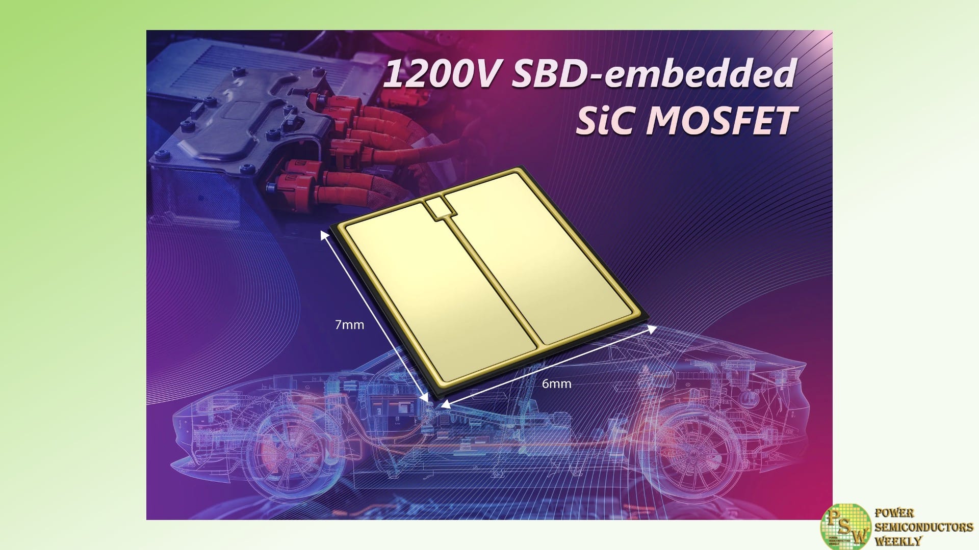
Toshiba Electronics Europe GmbH has developed new 1200V silicon carbide (SiC) MOSFETs with low on-resistance (RDS(ON)) and high levels of reliability. The devices are particularly suited to applications within automotive traction inverters. They are now available and shipping as early test samples in bare die format – allowing customers to customise them to meet the needs of their applications.
The new X5M007E120 uses a manufacturing process that reduces on-resistance per unit area by up to 30%. Unlike existing methods that utilise a striped-pattern construction, the new devices arrange the embedded Schottky barrier diodes (SBDs) in a check-pattern to achieve lower on-resistance.
Many SiC MOSFETs increase on-resistance as body diodes are energised during reverse conduction, which can lead to reliability issues. Toshiba SiC MOSFETs alleviate this issue by preventing body diodes from operating as SBDs are embedded into the MOSFETs. This approach maintains the reduction in on-resistance while ensuring reliability during reverse conduction.
With electric motors consuming over 40% of the world’s electrical energy, efficient operation is essential to sustainability. The re-arrangement of SBDs in this device has suppressed body diode energisation, and the upper limit of unipolar operation has increased to around double without increasing the SBD mounting area. Additionally, channel density is improved. These enhancements contribute to energy efficiency in applications, including motor control inverters.
Reducing RDS(ON) within a SiC MOSFET can cause excess current flow during short-circuit operations. By adopting a deep barrier structure, the X5M007E120 reduces excessive current within the MOSFET section and leakage current in the SBDs section during short-circuit operation. This enables durability during short-circuit conditions while maintaining high levels of reliability against reverse conduction operation.
The new X5M007E120 has a VDSS of 1200V and is rated for a drain current (ID) of 229A continuously, with 458A for pulsed operation (ID Pulse). RDS(ON) is as low as 7.2mΩ, and the device can operate with channel temperatures (Tch) as high as 175°C. The devices are AEC-Q100 qualified for automotive applications.
Engineering samples of the new X5M007E120 are expected to ship during 2025, with mass production samples scheduled to start in 2026.
Toshiba will continue to seek ways to further improve the characteristics of its products. The company will contribute to realising a decarbonised society by providing customers with power semiconductors for applications where energy efficiency is essential, such as inverters for motor control and power control systems for electrical vehicles.
Original – Toshiba
-
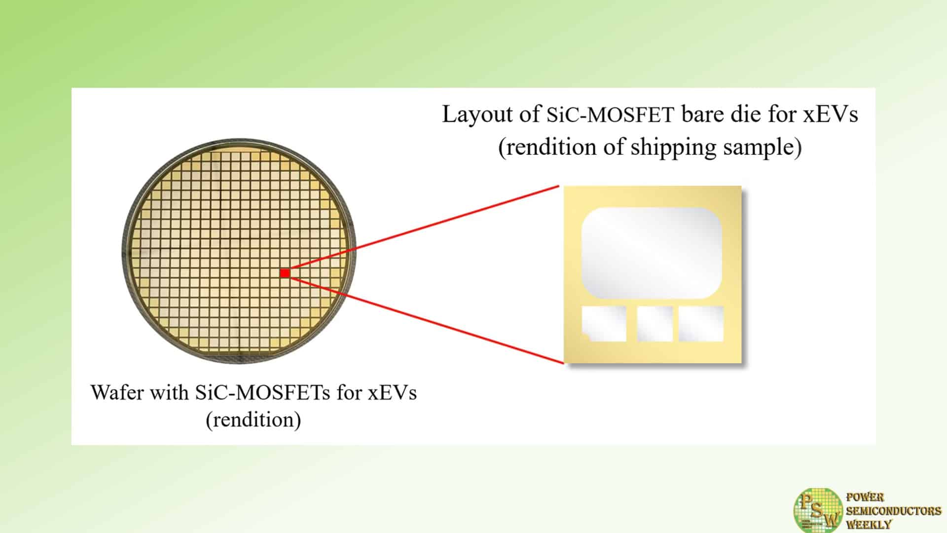
Mitsubishi Electric Corporation announced that it will begin shipping samples of a silicon carbide (SiC) metal-oxide-semiconductor field-effect transistor (MOSFET) bare die for use in drive-motor inverters of electric vehicles (EVs), plug-in hybrid vehicles (PHEVs) and other electric vehicles (xEVs) on November 14.
Mitsubishi Electric’s first standard-specification SiC-MOSFET power semiconductor chip will enable the company to respond to the diversification of inverters for xEVs and contribute to the growing popularity of these vehicles. The new SiC-MOSFET bare die for xEVs combines a proprietary chip structure and manufacturing technologies to contribute to decarbonization by enhancing inverter performance, extending driving range and improving energy efficiency in xEVs.
Mitsubishi Electric’s new power semiconductor chip is a proprietary trench SiC-MOSFET that reduces power loss by about 50% compared to conventional planar SiC-MOSFETs. Thanks to proprietary manufacturing technologies, such as a gate oxide film process that suppresses fluctuations in power loss and on-resistance, the new chip achieves long-term stability to contribute to inverter durability and xEV performance.
Original – Mitsubishi Electric
-

Stellantis N.V. and Infineon Technologies AG will work jointly on the power architecture for Stellantis’ electric vehicles to support Stellantis’ ambition of offering clean, safe and affordable mobility to all.
To support this, the companies have signed major supply and capacity agreements that will serve as the foundation for the planned collaboration to develop the next generation of power architecture, including:
- Infineon’s PROFET™ smart power switches, which will replace traditional fuses, reduce wiring and enable Stellantis to become one of the first automakers to implement intelligent power network management.
- Silicon carbide (SiC) semiconductors, which will support Stellantis in its efforts to standardize its power modules, improve the performance and efficiency of EVs while also reducing costs.
- AURIX TM microcontrollers, which target the first generation of the STLA Brain zonal architecture.
Stellantis and Infineon are also in the process of extending their cooperation with the implementation of a Joint Power Lab to define the next-generation scalable and intelligent power architecture enabling Stellantis’ software-defined vehicle.
“As outlined in our strategic plan, Dare Forward 2030, we are securing the supply of crucial semiconductor solutions required to continue our transition to an electrified future leveraging innovative E/E architectures for our next-generation platforms,” said Maxime Picat, Stellantis Chief Purchasing and Supplier Quality Officer.
“Infineon is now entering a collaboration and innovation partnership with Stellantis,” said Peter Schiefer, President of Infineon’s Automotive Division. “As the world’s leading automotive semiconductor vendor, we bring our product-to-system expertise and dependable electronics to the table. Our semiconductors drive the decarbonization and digitalization of mobility. They increase the efficiency of cars and enable software-defined architectures that will significantly improve the user experience.”
With the world`s most cost-competitive SiC fab in Kulim, Malaysia, the upcoming 300-millimeter ”Smart Power Fab” in Dresden, Germany, and the joint venture with TSMC and partners (ESMC) as well as accompanying supply agreements with foundry partners, Infineon is ready to fully meet market demand for automotive semiconductor solutions. According to the market research company TechInsights, Infineon is the global number one supplier of automotive microcontrollers with a market share of about 29 percent of the global automotive microcontroller market.
Original – Infineon Technologies
