-
Many different trends are taking center stage in both consumer electronics and industrial applications, such as portability, electrification, and weight reduction. All of these trends require compact and efficient designs. They also go hand in hand with unconventional PCB designs with severe space constraints that limit the use of external components.
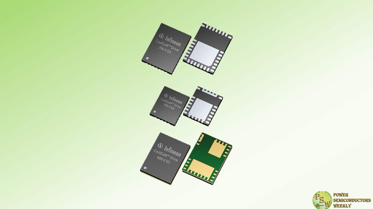
To address these challenges, Infineon Technologies AG expands its GaN portfolio with the CoolGaN™ Drive product family. It consists of the CoolGaN Drive 700 V G5 single switches, integrating one transistor plus gate driver in PQFN 5×6 and PQFN 6×8 packages, as well as the CoolGaN Drive HB 600 V G5 devices, combining two transistors with integrated high- and low-side gate drivers in a LGA 6×8 package. The new product family enables improved efficiency, reduced system size, and overall cost savings. This makes the devices suitable for longer-range e-bikes, portable power tools, and lighter-weight household appliances such as vacuums, fans, and hairdryers.
“For several years, Infineon has been focused on accelerating innovation in GaN to provide targeted solutions for real-world power challenges”, said Johannes Schoiswohl, Senior Vice President & General Manager, GaN Systems Business Line Head at Infineon. “The new CoolGaN Drive product family is another proof point of how we support our customers in developing compact designs with high power density and efficiency through GaN.”
The CoolGaN Drive family offers a wide range of single switches and half bridges with integrated drivers based on the recently announced CoolGaN Transistors 650 V G5. Depending on the product group, the components feature a bootstrap diode and are characterized by loss-free current measurement, and adjustable switch-on and switch-off dV/dt. They also provide OCP/OTP/SCP protection functions. As a result, the devices enable higher switching frequencies, leading to smaller and more efficient system solutions with high power density. At the same time, the bill of materials (BoM) is reduced. This not only results in a lower system weight, but also reduces the carbon footprint.
Samples of the half-bridge solutions are available now. Single-switch samples will be available starting Q4 2024. Further information is available at www.infineon.com/GaN-innovations.
Original – Infineon Technologies
-
According to a survey by Global Market Insights, Super Junction MOSFETs captured over 30% market share in the energy and power sector in 2023. Their applications span multiple domains, including electric vehicle charging stations, server and data center power supplies, LED drivers, solar inverters and home appliance controls.
The global Super Junction MOSFET market is projected to achieve a compound annual growth rate (CAGR) exceeding 11.5% by 2032. Super Junction MOSFETs offers robust assurance to customers seeking exceptional performance and stability backed by WeEn’s well-established reliability standards, comprehensive supply chain systems and continuously evolving technological roadmaps.
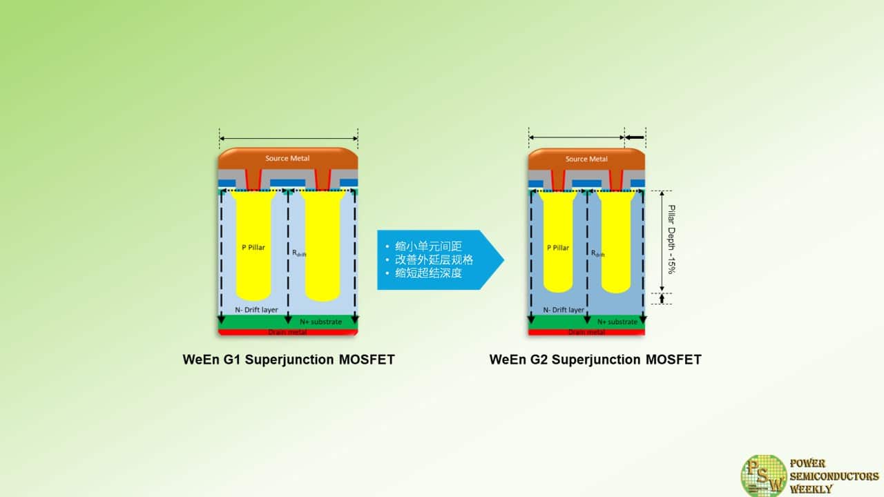
WeEn currently offers two series of Super Junction MOSFETs: G1 and G2. G2 Super Junction MOSFETs feature advanced design improvements, such as reduced cell pitch, low-resistance epitaxial layers, and shorter P-column depths. These innovations significantly reduce the device’s on-state resistance.
Simultaneously, WeEn precisely controlled the charge balance of the super junction structure, ensuring excellent avalanche ruggedness and low capacitive losses. This results in a balanced, outstanding performance in both hard and soft-switching applications that demand high efficiency, reliability, and superior thermal management.
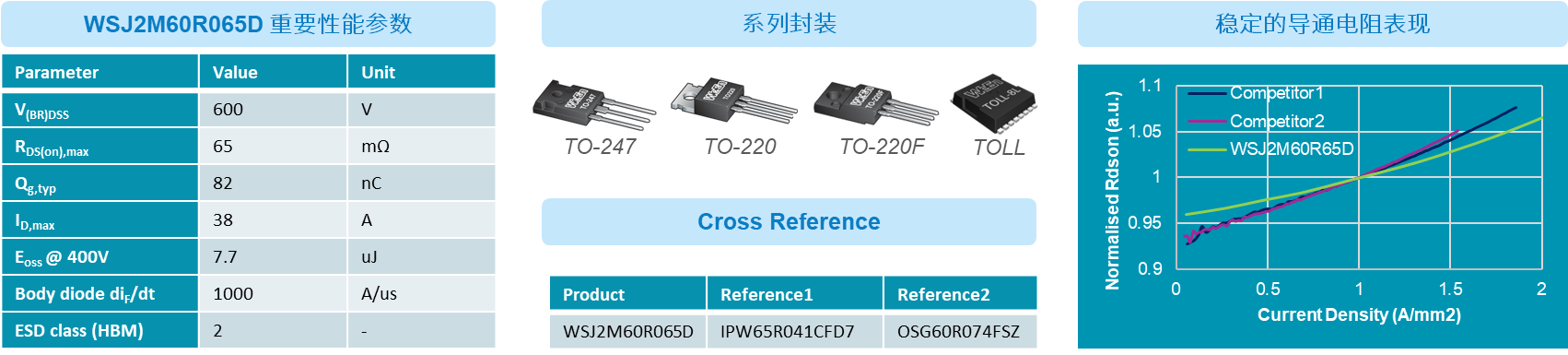
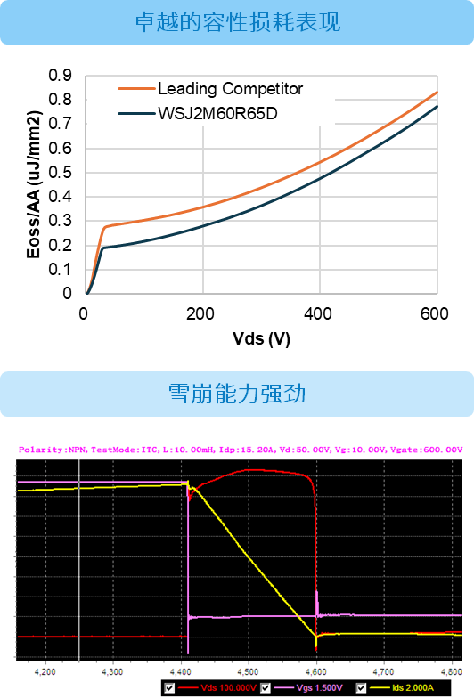
The WSJ2M60R065D is one of the flagship products in WeEn’s G2 Super Junction MOSFET lineup. Available in various packages including TO-220, TO-220F, TO-247, and TOLL. It particularly excels in terms of on-state resistance. Compared to competitors’ products, the WSJ2M60R065D maintains more stable on-state resistance across different current densities. Within its maximum continuous current range, the resistance variation does not exceed 10%. This stability provides customers with reliable performance data. Furthermore, the WSJ2M60R065D adapts well to applications with varying power requirements, demonstrating exceptional performance across diverse and complex operating environments.
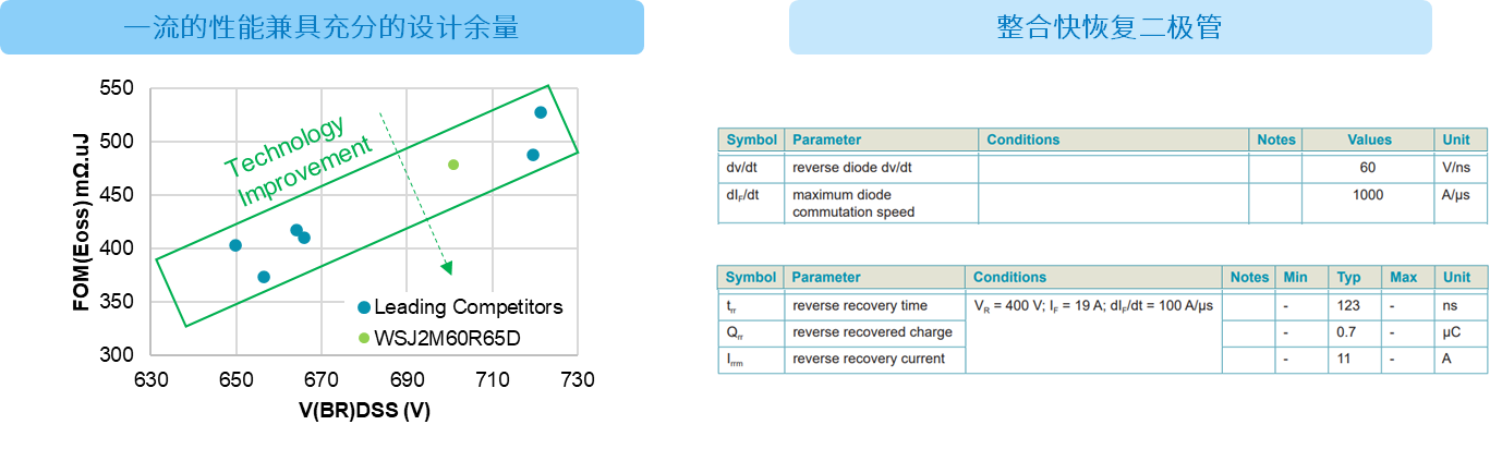
WeEn’s G2 MOSFETs are at the forefront of performance, with their Figure of Merit (FOM) on par with top global competitors. While ensuring stringent yield and process control, WeEn reserves more breakdown voltage margin for customers. 600V devices approach the standards of 650V devices available on the market, thoroughly safeguarding the reliability of customer applications. Moreover, the G2 MOSFET integrates a finely tuned fast recovery body diode, with a reverse recovery time (Trr) of only 123 ns. The body diode can withstand a commutation speed of 1000 A/μs without damage. This makes the WSJ2M60R065D particularly suitable for Zero Voltage Switching (ZVS) applications in soft-switching topologies, delivering high efficiency while handling irregular operating conditions.
However, the WSJ2M60R065D is not limited to soft-switching applications. It also demonstrates excellent performance in hard-switching applications. The WSJ2M60R065D offers significant advantages in terms of lower capacitive losses (Eoss) compared to top competitors. Additionally, its normalized ruggedness is significantly higher than the industry standard, enabling it to withstand higher overvoltage and oscillation. It also demonstrates stable and safe performance in hard-switching topologies such as Power Factor Correction (PFC) circuits.
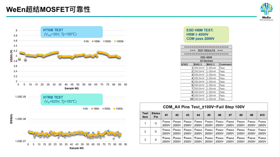
WeEn consistently adheres to rigorous and reliable quality assessment practices. In accelerated aging tests, the company maintains a zero-tolerance policy for product failures. WeEn MOSFET products demonstrate excellent consistency in performance during high-temperature stress aging tests at 168, 500, and 1000 hours. Furthermore, WeEn conducts additional reviews of the ESD (Electrostatic Discharge) capability of the device to minimize quality issues during production, packaging, and transportation. The WSJ2M60R065D demonstrates a robust quality level with a CDM (Charged Device Model) capability exceeding 2000V and an HBM (Human Body Model) capability of over 4000V.
Original – WeEn Semiconductors
-

VisIC Technologies Ltd. has partnered with Heraeus Electronics and PINK to develop an advanced power module utilizing D3GaN technology. This groundbreaking power module is based on a silicon nitride (Si₃N₄) ceramic substrate, an innovative silver (Ag) sintering process and advanced top side interconnect, promising unprecedented reliability and performance for battery electric vehicles (BEVs).
The collaboration brings together VisIC’s expertise in GaN-based devices, Heraeus Electronics’ cutting-edge packaging materials know-how, and PINK’s state-of-the-art sintering technology. The synergy of these industry leaders has culminated in the development of a power module that is setting new standards for GaN based power modules to revolutionize the EV industry.
VisIC’s D3GaN technology is at the heart of this power module, offering significant improvements in efficiency, thermal management, and power density. This technology leverages the superior electrical properties of gallium nitride to deliver faster switching speeds and higher power handling capabilities compared to traditional silicon-based devices.
The use of a Si₃N₄ metal ceramic substrate is a key innovation in this power module. Si₃N₄ is known for its excellent thermal conductivity, mechanical strength, and reliability under high-temperature conditions. These properties are crucial for the demanding environment of electric vehicle applications, ensuring the power module can withstand the rigors of everyday use while maintaining optimal performance.
The adoption of the silver sintering process by PINK enhances the thermal and electrical conductivity of the module. Silver sintering is a low-temperature bonding process that creates robust and reliable connections between components, improving the module’s overall durability and efficiency. This process is critical for the high reliability required in EV powertrains, where consistent performance is non-negotiable.
The resulting power module is designed to meet the stringent reliability and performance standards of the electric vehicle industry. Its advanced materials and innovative construction techniques ensure it can deliver the high-power density of over 500Arms/650V and efficiency needed for modern BEVs, while also offering long-term reliability and durability at a cost point near silicon devices.
This collaboration marks a significant milestone in the advancement of power electronics for electric vehicles. The integration of VisIC’s D3GaN technology with Heraeus Electronics’ sintering paste and PINK’s Ag and Cu sintering process and flexible sintering equipment sets a new benchmark for power module performance in the EV market. This innovation is expected to drive the adoption of GaN technology in EV applications, paving the way for more efficient, reliable, and sustainable electric transportation solutions.
Tamara Baksht, CEO of VisIC, state: “We are thrilled to work with the leading manufacturer of sintering processes of Heraeus Electronics and PINK and adapt their experience into GaN based power modules to develop the next generation of power module for high volume automotive inverter applications.”
PINK, Andrea Pink, CEO of PINK statement: “We are excited to work with such a future driven company as VisIC together with our long-term partner Heraeus Electronics, supporting the newest product innovation for GaN applications.”
Heraeus Electronics Dr. Michael Jörger, EVP Head of Business Line Power Electronic Materials added: “With our materials, application know-how and engineering services we are glad to work with our partners on speeding up the innovative approach of highly efficient GaN modules for automotive applications.”
Original – VisIC Technologies
-

Toshiba Electronic Devices & Storage Corporation and Toshiba Corporation (Toshiba Group) have developed technology that mitigates the parasitic oscillation that occurs during switching operations by power modules with silicon carbide (SiC) MOSFETs connected in parallel, even with a 60% smaller gate resistance than is typical. The technology reduces power loss in power modules, mitigates oscillation, and realizes highly reliable switching operations.
The drive for carbon neutrality is stimulating demand for technologies that improve energy efficiency in many areas, including renewables, railways, and industrial equipment. In these sectors, the application of power modules built around SiC MOSFETs is seen as a solution that supports high-speed switching at high voltages and large currents—which is particularly important for the miniaturization of power converters, where higher switching frequencies result in higher rates of switching losses against power consumption.
Connecting multiple chips in parallel in power modules can form oscillation circuits, the result of wiring inductance between the chips and their parasitic capacitance. It can reduce module reliability if not countered, which is usually done by increasing gate resistance. However, this approach slows switching speed, resulting in a trade-off with switching losses. For power modules with SiC MOSFETs to perform high-speed switching, another approach is needed.
Toshiba Group used an equivalent circuit model of the power module (Figure 1) to determine the theoretical condition that triggers parasitic oscillation, and developed a wiring layout less likely to cause it. This was done by analyzing simulations of parasitic oscillation occurs when Lg/Ls, the ratio of gate-to-gate inductance Lg and source-to-source inductance Ls of parallel chips, is below a certain value (Figure 2). As increasing Lg/Ls is an effective means of mitigating parasitic oscillation, Toshiba Group fabricated prototype modules with different Lg/Ls and measured switching. This confirmed that increasing Lg/Ls mitigated oscillation, even with a 60% smaller gate resistance than that required by the alternative approach of increasing gate resistance (Figure 3).
Applying this approach to oscillation mitigation in power modules now under development has realized a power module less likely to cause parasitic oscillation, even with minimal gate resistance, that achieves low power loss with mitigated oscillation, and delivers highly reliable switching operation. Toshiba Group will continue to make refine the modules toward an early product launch.
Toshiba Group presented the details of this technology on June 6 at the 36th International Symposium on Power Semiconductor Devices and ICs (ISPSD) 2024, an international power semiconductor conference held in Bremen, Germany from June 2 to 6.
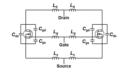
Figure 1. Model equivalent circuit of two MOSFETs connected in parallel 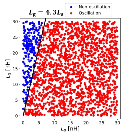
Figure 2. Simulation of oscillation in two MOSFETs with zero gate resistance connected in parallel 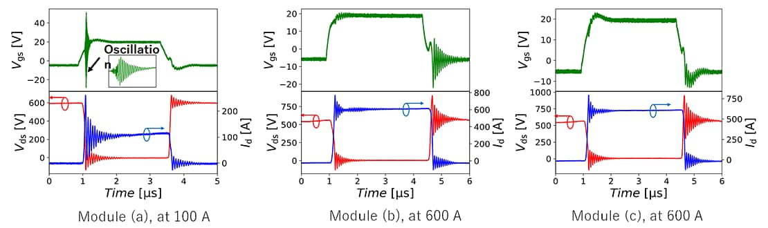
Vgs: Gate-Source voltage, Vds: Drain-Source voltage, Id: Drain current
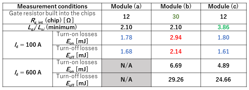
Figure 3. Switching waveforms and switching losses of the prototype modules (Source: Toshiba Group tests) Original – Toshiba
-

onsemi has signed a multi-year deal with Volkswagen Group to be the primary supplier of a complete power box solution as part of its next-generation traction inverter for its Scalable Systems Platform (SSP). The solution features silicon carbide-based technologies in an integrated module that can scale across all power levels – from high power to low power traction inverters to be compatible for all vehicle categories.
“By offering a complete power system solution that encompasses the entire power sub-assembly, we provide Volkswagen Group with a single, simplified modular and scalable platform that maximizes efficiency and performance for their vehicle lineup,” said Hassane El-Khoury, president and CEO of onsemi. “This new approach allows for the customization of power needs and the addition of features for different vehicles without compromising on performance, all while reducing cost.”
Based on the EliteSiC M3e MOSFETs, onsemi’s unique power box solution can handle more power in a smaller package which significantly reduces energy losses. The inclusion of three integrated half-bridge modules mounted on a cooling channel will further improve system efficiency by ensuring heat is effectively managed from the semiconductor to the coolant encasement.
This leads to better performance, improved heat control, and increased efficiency, allowing EVs to drive further on a single charge. By using this integrated solution, Volkswagen Group will be able to easily transition to future EliteSiC-based platforms and remain at the forefront of EV innovation.
“We are very pleased to have onsemi as a strategic supplier for the power box of the traction inverter for our first tranche in the SSP platform. onsemi has convinced us with a deeply verticalized supply chain from the growth of the raw material up to the assembly of the power box,” said Mr. Dirk Große-Loheide, Member of the Extended Executive Committee Group Procurement and Member of the Board Volkswagen Brand for “Procurement”.
Mr. Till von Bothmer, Senior Vice President VW Group Procurement for Powertrain added, “On top of the verticalization, onsemi has furthermore provided a resilient supply concept with regional silicon carbide fabs across Asia, Europe and the U.S. In addition, onsemi will continuously provide the latest SiC generation to ensure competitiveness.
Volkswagen Group will also benefit from onsemi’s planned investment to expand its silicon carbide manufacturing in the Czech Republic. The investment would establish an end-to-end production facility in Europe for the traction inverter power system. The proximity of onsemi’s facility would fortify Volkswagen Group’s supply chain while improving logistics and allowing for faster integration into the manufacturing process.
Original – onsemi
-

Infineon Technologies AG announced that its CoolSiC™ 2000 V modules have been selected by Daihen Corporation for their innovative unit-type power conditioners for grid storage batteries. In the journey towards reducing carbon emissions, both grid storage batteries and the power conditioners that are linked to them play a vital role in facilitating the wider adoption of renewable energy sources like solar and wind power generation.
There has been an increasing demand for higher voltage storage batteries and power conditioners to enhance the effectiveness of power generation, storage, and transmission. Moreover, with the expansion of storage battery systems on a larger scale, finding suitable locations and minimizing construction costs have emerged as significant challenges.
The unit-type power conditioner for grid storage batteries launched by Daihen in March 2024 is the first product in the industry to achieve connection to storage batteries at a high DC link voltage of 1500 V. The higher voltage enables the product to be used with large-capacity storage battery facilities, which has resulted in a 40% reduction in the footprint of grid storage batteries compared to the conventional product.
The high power density is achieved by using Infineon’s 62 mm CoolSiC MOSFET 2000 V module (FF3MR20KM1H). In addition to the characteristics of SiC that enable high voltage, better thermal dissipation and high power density, Infineon’s SiC products feature M1H trench technology that increases the gate drive voltage range and provides high robustness and reliability against gate voltage spikes. Infineon was the pioneer in the industry to introduce the 2000 V class for a SiC module. This innovation has been instrumental in simplifying the inverter circuit configuration. Furthermore, the optimized 62 mm package has led to a substantial reduction in system size, contributing to enhanced efficiency and performance.
Mr. Akihiro Ohori, General Manager, Development Department, Energy Management System Division, Daihen, said, “In order to increase the voltage of power conditioners, the circuit configuration of conventional 1200 V devices had become complicated. However, by adopting Infineon’s 2000 V SiC modules, we were able to achieve a simplified circuit configuration and control design, thereby reducing development resources and the footprint.”
Masanori Fujimori, Marketing Director of the Industrial & Infrastructure Segment at Infineon Technologies Japan, said, “We are very pleased that our pioneering CoolSiC 2000 V module has contributed to the development of the industry’s highest power density power conditioners for grid storage batteries. We believe that Infineon’s SiC technology will address the need for higher efficiency in energy storage systems and will greatly contribute to the growth of renewable energy.”
Original – Infineon Technologies
-

Power Master Semiconductor has released 2nd generation of the 1200V eSiC MOSFET to meet the requirements of higher efficiency, high power density, robust reliability, and ruggedness in various applications such as DC EV charging stations, solar inverters, energy storage systems (ESS), motor drives and industrial power supplies. 1200V eSiC MOSFETs offer significant system advantages such as higher power density, efficiency and less cooling effort due to its much lower power losses.
Therefore, SiC MOSFETs are gaining popularity especially for renewable energy systems, EV charging systems that required higher power density, efficiency and robustness. DC EV charging station is level-3 charger and its power level is increasing by modular configuration as demand of faster charging time and higher battery capacity of EV. DC EV charging provides a mostly constant current output for wide DC output voltage range (200V to 900V) and load profile.
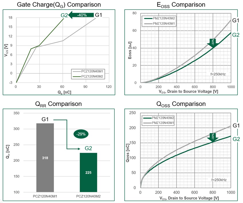
The new generation of 1200V eSiC MOSFET, Gen2 improved key FOM characteristics such as gate charge (QG), stored energy in output capacitance (EOSS), reverse recovery charger (QRR) and output charge (QOSS) by up to 30% compared to previous generation. This new generation SiC MOSFET technology offers significant system advantages such as smaller, lighter, higher efficiency, and less cooling effort thanks to its much lower power losses in various power conversion applications.
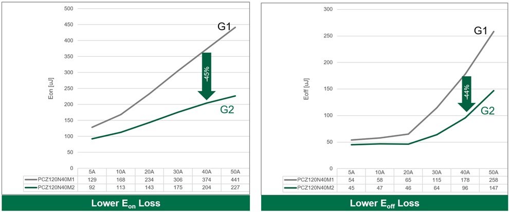
1200V eSiC MOSFET Gen2 offer excellent switching performance and 100% tested avalanche capability. It achieved 44% lower switching loss compared to the previous generation by extremely low miller capacitance (QGD).
Power Master Semiconductor is steadfastly committed to developing cutting-edge power device solutions that prioritize efficiency and sustainability,” said Namjin Kim, Sr. Director Sales & Marketing. “The introduction of our new generation of 1200V eSiC MOSFET marks a substantial leap forward in facilitating the development of cleaner, more efficient power systems. We are confident that the 1200V eSiC Gen2 MOSFET will play a transformative role in high-performance applications.
Original – Power Master Semiconductor
-

In the face of escalating climate crises and a dramatic rise in global energy demands, governments and industries are committing to ambitious climate goals aimed at mitigating environmental impact and securing a sustainable future. Key to these efforts is the transition to electrification to reduce carbon emissions and embrace renewable energy resources.
In a significant step towards accelerating this global transition, onsemi introduced its latest generation silicon carbide technology platform, EliteSiC M3e MOSFETs. The company also disclosed plans to release multiple additional generations through 2030.
“The future of electrification is dependent on advanced power semiconductors. Today’s infrastructure cannot keep up with the world’s demands for more intelligence and electrified mobility without significant innovations in power. This is critical to the ability to achieve global electrification and stop climate change,” said Simon Keeton, group president, Power Solutions Group, onsemi. “We are setting the pace for innovation, with plans to significantly increase power density in our silicon carbide technology roadmap through 2030 to be able to meet the growing demands for energy and enable the global transition to electrification.”
The EliteSiC M3e MOSFETs will play a fundamental role in enabling the performance and reliability of next-generation electrical systems at lower cost per kW, thus influencing the adoption and effectiveness of electrification initiatives. With the ability to operate at higher switching frequencies and voltages while minimizing power conversion losses, this platform is essential for a wide range of automotive and industrial applications such as electric vehicle powertrains, DC fast chargers, solar inverters and energy storage solutions.
Additionally, the EliteSiC M3e MOSFETs will enable the transition to more efficient, higher-power data centers to meet the exponentially increasing energy demands that power a sustainable artificial intelligence engine.
Through onsemi’s unique design engineering and manufacturing capabilities, the EliteSiC M3e MOSFETs achieve a significant reduction in both conduction and switching losses on the trusted and field-proven planar architecture. Compared to previous generations, the platform can reduce conduction losses by 30% and turn-off losses by up to 50%.
By extending the life of SiC planar MOSFETs and delivering industry-leading performance with EliteSiC M3e technology, onsemi can ensure the robustness and stability of the platform, making it a preferred choice for critical electrification applications
The EliteSiC M3e MOSFETs also offer the industry’s lowest specific on-resistance (RSP) with short circuit capability which is critical for the traction inverter market that dominates SiC volume. Packaged in onsemi’s state-of-the-art discrete and power modules, the 1200V M3e die delivers substantially more phase current than previous EliteSiC technology, resulting in approximately 20% more output power in the same traction inverter housing. Conversely, a fixed power level can now be designed with 20% less SiC content, saving costs while enabling the design of smaller, lighter and more reliable systems.
Additionally, onsemi provides a broader portfolio of intelligent power technologies including gate drivers, DC-DC converters, e-Fuses and more to pair with the EliteSiC M3e platform. The end-end onsemi combination of optimized, co-engineered power switches, drivers and controllers enable advanced features via integration, lowering overall system cost.
Global energy demands are projected to soar over the next decade, making the need for increased power density in semiconductors paramount. onsemi is leading innovation across its silicon carbide roadmap – from die architectures to novel packaging techniques – that will continue to address the general industry demand for increased power density.
With each new generation of silicon carbide, cell structures will be optimized to efficiently push more current through a smaller area, increasing power density. When coupled with the company’s advanced packaging techniques, onsemi will be able to maximize performance and reduce package size.
By applying the concepts of Moore’s Law to the development of silicon carbide, onsemi can develop multiple generations in parallel and accelerate its roadmap to bring several new EliteSiC products to market at an accelerated pace through 2030.
“We are applying our decades of experience in power semiconductors to push the boundaries of speed and innovation in our engineering and manufacturing capabilities to meet the rising global energy demands,” said Dr. Mrinal Das, senior director of technical marketing, Power Solutions Group, onsemi. “There is a huge technical interdependency between the materials, device and package in silicon carbide. Having full ownership over these key aspects allows us to have control over the design and manufacturing process and bring new generations to market much faster.”
The EliteSiC M3e MOSFET in the industry-standard TO-247-4L package is now sampling.
Original – onsemi
-

GlobalWafers Co., Ltd. announced that GWC subsidiaries, GlobalWafers America (GWA) and MEMC LLC, have signed a non-binding preliminary memorandum of terms (PMT) with the U.S. Department of Commerce for up to $400 million in direct funding under the CHIPS and Science Act to support GWC’s construction of advanced silicon wafer manufacturing facilities in Sherman, Texas and St. Peters, Missouri.
When complete, the Sherman, Texas complex will be the first fully integrated advanced silicon wafer production line built in the United States in over 20 years. GWA President Mark England remarked, “With the support of the Biden Administration, we are honored to be bringing to American shores the world’s most cutting-edge 300mm semiconductor wafer technology, filling what the White House has called a “key vulnerability” within the U.S. semiconductor supply chain. GlobalWafers is fully committed to the U.S. market, and we are excited to be playing a defining role in the nation’s semiconductor rebirth.”
With this proposed investment, GWA will also become a key node in Texas’s rapidly developing Silicon Prairie ecosystem. England added, “The state of Texas and the North Texas Texoma region have welcomed GWA with open arms and investment incentives. We are proud to reciprocate their hospitality by bringing to Sherman 1200 construction jobs and 750 high paying manufacturing jobs ranging from production operators to technicians and engineers between now and 2026.” As the only confirmed advanced node wafer manufacturer now investing in the United States, GWA will reduce the United States’ complete dependence on overseas manufacturing facilities to provide wafers for advanced chips.
Already home to semiconductor pioneer Texas Instruments (TI), the GlobalWafers investment will help make North Texas the most unique semiconductor ecosystem in the country as headquarters to the nation’s leading analogue and embedded semiconductor company AND home to the country’s only 300-mm silicon wafer manufacturer for advanced chips. TI Vice President of Worldwide Procurement and Logistics Rob Simpson congratulated both GlobalWafers and the U.S. Department of Commerce on this announcement, noting: “TI welcomes the investment in GlobalWafers America in North Texas, as it will be a very meaningful addition to the growing semiconductor ecosystem here.”
“Texas continues to lead the country as the Best State for Business,” said Governor Greg Abbott. “Companies like GlobalWafers America – the only advanced node wafer manufacturer in the U.S. – are investing in Texas because of our world-class business climate, business-friendly regulations, and young, growing, and highly skilled workforce. GlobalWafers is a crucial partner in our efforts to remain the nation’s No. 1 state for semiconductor manufacturing, and I thank them for choosing North Texas for their new facility.”
In support of national economic and resilience objectives, GWC is committed to developing in the United States a broad range of next-generation wafer technology. This includes establishing a Research and Development Center of Excellence in Sherman as well as building the United States’ only 300-mm manufacturing facility for advanced Silicon-On-Insulator (SOI) wafers at GWC’s MEMC LLC subsidiary in St. Peters, Missouri where the project brings an additional 500 construction jobs and 130 high quality manufacturing jobs.
As the only U.S. source of 300-mm SOI wafers, the MEMC investment will add a new level of resilience to the U.S. supply chain. On this point, Ashlie Wallace, Senior Vice President of Global Supply Chain at GlobalFoundries observed, “GlobalFoundries applauds the proposed CHIPS direct funding to GlobalWafers, a longstanding strategic partner of ours which provides an important domestic supply of silicon wafers critical for the essential semiconductors we manufacture.” Wallace added, “Federal investments across the U.S. semiconductor ecosystem are strengthening our industry and the supply chains that are vital to our customers and the economy.”
Noting the significance of this proposed funding to U.S. supply chain resilience efforts, U.S. Secretary of Commerce Gina Raimondo said, “President Biden is restoring our leadership in the entire semiconductor supply chain – from materials to manufacturing, to R&D. With this proposed investment, GlobalWafers will play a crucial role in bolstering America’s semiconductor supply chain by providing a domestic source of silicon wafers that are the backbone of advanced chips. As a result of this proposed investment, the Biden-Harris Administration is helping to secure our supply chains, which will create over 2,000 jobs across Texas and Missouri and ultimately lower costs and improve economic and national security for Americans.”
In addition to the direct grant funding announced today, GWC plans to apply for the U.S. Treasury Department’s Advanced Manufacturing Investment Credit (AMIC) of up to 25% of qualified expenditures at the GWA and MEMC LLC facilities.
From Hsinchu, Taiwan, GlobalWafers Chairwoman and CEO Doris Hsu expressed her personal thanks to the U.S. Congress, the Department of Commerce, and the Department of Treasury for CHIPS Act support: “Thanks to U.S. Government support, GlobalWafers is pleased to be a key node in the U.S. semiconductor supply chain. I’d like to particularly thank Secretary Raimondo for her partnership and vision throughout this journey. From day one, her encouragement gave me confidence that U.S. Government support for our investment would be significant and strategic to U.S. objectives.”
As a key ESG imperative, GlobalWafers companies across the globe practice green manufacturing and constantly seek to improve energy efficiency, water conservation, waste management and air pollution control. When at full ramp, GWC’s new and expansion facilities in Sherman and St. Peters will recycle up to half of the water used in production and have forward plans to utilize 100% renewable energy to manufacture the world’s most advanced silicon wafers. The GlobalWafers family of companies is committed to reducing our environmental footprint to the fullest extent possible.
GlobalWafers Co., Ltd., the world’s third largest supplier of semiconductor wafers, maintains 18 manufacturing and operational sites spanning three continents and nine countries. The company is a global leader in semiconductor technology, providing innovative and advanced technology solutions to leading chip manufacturers to transform lives around the world.
Original – GlobalWafers
-
 LATEST NEWS / PROJECTS / SiC / TOP STORIES / WBG
SiCrystal’s SiC Wafers Production Capacity to Triple by 2027 with a New Production Site in Nuremberg
July 4, 2024
2 Min ReadIn an important step towards strengthening the semiconductor industry and promoting sustainable technologies, SiCrystal GmbH will create new, additional production space in the north-east of Nuremberg, directly opposite the existing site. The new building will offer an additional 6,000 square meters of production space and will be equipped with state-of-the-art technology to further optimize the production of silicon carbide wafers.
The close proximity to the existing plant will ensure close integration of the production processes. SiCrystal’s total production capacity, including the existing building, will be approximately three times higher in 2027 than in 2024.
“The new space will significantly increase the production capacity for SiC substrates and we are proud that we were able to welcome Mayor König to the ground-breaking ceremony,” says Dr. Robert Eckstein, CEO of SiCrystal. This underlines the importance of this project for the city and the region.
“This groundbreaking ceremony marks an important milestone for SiCrystal and underlines our commitment to the metropolitan region. In this way, we can continue to supply innovative products of the highest quality for our customers in the future and make a positive contribution to global sustainability. “, said Dr. Erwin Schmitt, COO of SiCrystal. “With the additional production capacities, we will strengthen our market position and make an important contribution to technological development in the semiconductor industry.”
Nuremberg’s Mayor Marcus König congratulates on this event: “SiCrystal is one of the world’s leading manufacturers of silicon carbide semiconductor substrates – among other things, these products are needed for the energy transition. I am delighted that SiCrystal is committing itself to Nuremberg as a location with this massive investment and is thus not only retaining jobs but also creating new ones. Nuremberg is an attractive location.”
The construction work is scheduled to be completed by the beginning of 2026. And will create new jobs in the region. The new building is being realized in cooperation with the general contractor Systeambau from Hilpoltstein.
SiC wafers from SiCrystal, a subsidiary of the Japanese ROHM Group, are of crucial importance for the production of high-performance semiconductor components. By using SiC, we can achieve higher efficiency, lower energy consumption and improved performance in various applications such as electric vehicles, solar energy, and industrial equipment.
SiCrystal is proud to be a fast-growing employer in the metropolitan region and aims to increase employment by more than 100 by the end of the 2027/28 financial year.
Original – SiCrystal
