-

Navitas Semiconductor announced the release of its latest SiCPAK™ power modules with epoxy-resin potting technology, powered by proprietary trench-assisted planar SiC MOSFET technology, that have been rigorously designed and validated for the most demanding high-power environments, prioritizing reliability and high-temperature performance. Target markets include EV DC fast chargers (DCFC), industrial motor drives, interruptible power supplies (UPS), solar inverters and power optimizers, energy storage systems (ESS), industrial welding, and induction heating.
The new portfolio of 1200V SiCPAK™ power modules, enabled by advanced epoxy-resin potting technology, are engineered to withstand high-humidity environments by preventing moisture ingression and enable stable thermal performance by reducing degradation from power and temperature variations.
Navitas’ SiCPAK™ modules demonstrated 5x lower thermal resistance increase following 1000 cycles of thermal shock testing (-40 C to + 125 C) compared to conventional silicone-gel-filled case-type modules. Furthermore, all silicone-gel-filled modules failed isolation tests while SiCPAK™ epoxy-resin potted modules maintained acceptable isolation levels.
Enabled by over 20 years of SiC innovation leadership, Navitas’ GeneSiC™ ‘trench-assisted planar SiC MOSFET technology’ provides industry-leading performance over temperature, enabling up to 20% lower losses, cooler operation, and superior robustness to support long-term system reliability.
The ‘trench-assisted planar’ technology enables an extremely low RDS(ON) increase versus temperature, which results in the lowest power losses across a wider operating range and offers up to 20% lower RDS(ON) under in-circuit operation at high temperatures compared to competition. Additionally, all GeneSiC™ SiC MOSFETs have the highest-published 100%-tested avalanche capability, up to 30% better short-circuit withstand energy, and tight threshold voltage distributions for easy paralleling.
The 1200V SiCPAK™ power modules have built-in NTC thermistors and are available from 4.6 mΩ to 18.5 mΩ ratings in half-bridge, full-bridge, and 3L-T-NPC circuit configurations. They are pin-to-pin compatible with industry-standard press-fit modules. Additionally, optional pre-applied Thermal Interface Material (TIM) for simplified assembly is available.
Original – Navitas Semiconductor
-

Polar Semiconductor announced the finalization of a strategic agreement with Renesas Electronics Corporation to license their Gallium Nitride on Silicon D-Mode (GaN-on-Si) technology. As part of this agreement, Polar will fabricate High Voltage 650V Class GaN-on-Si devices for Renesas and other customers in its 200mm automotive quality high-volume manufacturing facility in Minnesota. This facility, recently expanded with state-of-the-art processing and automation equipment, is poised to meet growing demand for next-generation semiconductor solutions.
Polar and Renesas will work together to scale commercial production of GaN devices, expanding its use across critical industries, including automotive, data center, consumer, industrial, and aerospace & defense markets. The agreement ensures the U.S. has a reliable, domestic source for this cutting-edge semiconductor technology.
Market adoption of GaN technology will be accelerated through cost efficiency and innovative device architectures enabled by scaling to 200mm fabrication. By leveraging Polar’s manufacturing expertise and Renesas’ proven power semiconductor technology and commercial leadership, this strategic collaboration ensures customers a secure supply of cost-competitive, superior quality, and high-performance GaN device wafers.
Surya Iyer, President and COO of Polar Semiconductor, said, “This licensing and commercial production agreement underscores our commitment to strengthening the domestic semiconductor ecosystem. GaN is a game-changing technology for Power and RF, and with Renesas as our partner, we are well-positioned to ramp commercial production, secure key defense programs, and drive the next wave of semiconductor innovation.”
“We are excited to partner with Polar to scale our proven GaN technology to 200mm wafers and leverage our know-how across broad power conversion markets ranging from Infrastructure & AI to Energy & Industrial to e-Mobility & xEVs to high-value IoT,” said Chris Allexandre, SVP & GM, Power Products Group, at Renesas. “This collaboration ensures a strong, U.S.-based manufacturing capability for GaN products, provides multi-sourcing to our customers, and meets the growing demand for high-performance power solutions.”
Original – Polar Semiconductor
-

Mitsubishi Electric Corporation announced that it will begin shipping samples of two new SLIMDIP series power semiconductor modules for room air conditioners and other home appliances, the Full SiC (silicon carbide) SLIMDIP (PSF15SG1G6) and the Hybrid SiC SLIMDIP (PSH15SG1G6), on April 22.
Both modules, the first SiC versions in the company’s SLIMDIP series of compact, terminal-optimized modules, achieve excellent output and power loss reduction for energy savings in small- to large-capacity appliances. They will be exhibited at Power Conversion Intelligent Motion (PCIM) Expo & Conference 2025 in Nuremberg, Germany from May 6 to 8, as well as trade shows in Japan, China and other countries.
Mitsubishi Electric’s newly developed silicon carbide metal-oxide-semiconductor field-effect transistor (SiC-MOSFET) chip is incorporated into both new SLIMDIP packages. Compared to current silicon (Si)-based reverse-conducting insulated-gate bipolar transistor (RC-IGBT) SLIMDIP modules, these new SiC modules achieve higher output for larger-capacity appliances. Additionally, compared to the Si-based module, power loss is reduced by 79% with the Full SiC SLIMDIP and by 47% with the Hybrid SiC SLIMDIP for more energy-efficient appliances.
With these two new modules as well as existing Si-based RC-IGBT SLIMDIP modules, the SLIMDIP series now offers three options for use in inverter boards of appliances such as room air conditioners, each one suited to specific electrical capacity and performance needs, but all offered in the same package to help reduce the burden of designing inverter substrates.
Original – Mitsubishi Electric
-
 LATEST NEWS / PRODUCT & TECHNOLOGY / SiC / WBG
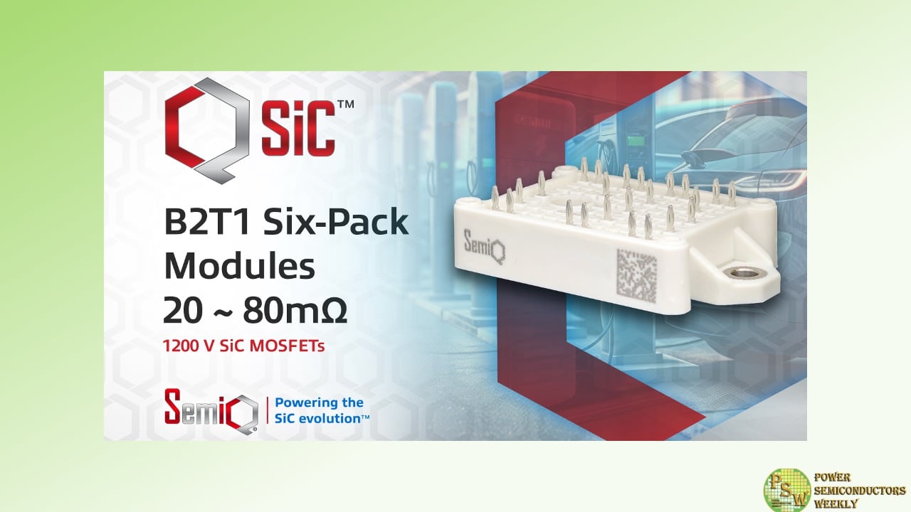
SemiQ Launches High-Efficiency 1200V SiC MOSFET Six-Pack Modules for Scalable, Compact Power Designs
April 16, 2025
2 Min ReadSemiQ Inc has announced a series of highly efficient 1200 V SiC MOSFET Six-Pack Modules. These have been designed to enable lower cost and more compact system-level designs at large scale.
The rugged, high-speed switching SiC MOSFETs implement a planar technology with rugged gate oxide and feature a reliable body diode. These are arranged in a three-phase bridge topology, with the modules additionally featuring split DC negative terminals, press-fit terminal connections and a Kelvin reference for stable operation.
The high-power-density modules benefit from low switching losses, as well as low junction-to-case thermal resistance and all parts have been tested beyond 1350 V, with 100% wafer-level burn in (WLBI).
They have been developed for applications including AC/DC converters, energy storage systems, battery charging, motor drives and PFC boost converters, including EV fast charging, induction heating and welding, renewable energy supplies and UPS.
The modules are operational to 175oC junction temperature, and have been designed for easy mounting, including direct mounting to a heatsink. The product family has been launched with 20, 40 and 80mΩ variants (GCMX020A120B2T1P, GCMX040A120B2T1P, GCMX080A120B2T1P) that have a power dissipation of 263, 160 and 103 W respectively.
They conduct a continuous drain current of 29 – 30A, and a pulsed drain current of 70 A. Additionally, they have turn-on switching energy of 0.1- 0.54 mJ and a turn-off switching energy of 0.02 – 0.11 mJ, with a switching time of 56 – 105 ns.
The module is available immediately in a 62.8 x 33.8 x 15 mm package including heatsink mountings.
Original – SemiQ
-

Navitas Semiconductor has announced its high-power GaNSafe™ ICs achieve automotive qualification for both AEC-Q100 and AEC-Q101, showcasing GaN’s next inflection into the automotive market.
Navitas high-power GaNSafe 4th generation family integrates control, drive, sensing, and critical protection features that enable unprecedented reliability and robustness in high-power applications. It is the world’s safest GaN with short-circuit protection (350ns max latency), 2kV ESD protection on all pins, elimination of negative gate drive, and programmable slew rate control. All these features are controlled with 4-pins, allowing the package to be treated like a discrete GaN FET, requiring no VCC pin.
The Automotive Electronics Council (AEC) lists various qualifications focused on failure mechanism-based stress tests for packaged integrated circuits (AEC-Q100) and discrete semiconductors (AEC-Q101) used in automotive applications. Navitas’ GaNSafe™ has been qualified to both standards to ensure that both the discrete power FET stage and the combined IC solution meet these stringent specifications.
To support the qualification, Navitas has created a comprehensive reliability report that analyzes over 7 years of production and field data. It demonstrates their track record, alongside generational and family improvements in robustness and reliability, establishing GaN power ICs as highly reliable and automotive-ready. This reliability report is available to qualified customers.
Additionally in March 2025, Navitas unveiled the world’s first production released 650V Bi-Directional GaNFast ICs with IsoFast Drivers, creating a paradigm shift in power to enable the transition from two-stage to single-stage topologies to further enhance efficiency, power density, and performance in AC-DC and AC-AC conversion. This would allow next-generation single-stage OBCs to provide bi-directional charging in a high-efficiency, extremely compact solution – which eliminates bulky capacitors and input inductors.
A leading EV and solar micro-inverter manufacturer have already begun their implementation of single-stage BDS converters to improve efficiency, size, and cost in their systems. GaNFast-enabled single-stage BDS converters achieve up to 10% cost savings, 20% energy savings, and up to 50% size reductions.
“Our latest reliability report is the culmination of years of innovation and field experience,” said Gene Sheridan, CEO and co-founder of Navitas. “With more than 250 million units shipped, over 2 trillion field devices hours and a cumulative field failure rate that is now approaching 100 parts per billion, we’re leading the charge in making GaN the go-to technology for EV power systems.”
Original – Navitas Semiconductor
-

Diodes Incorporated announced the expansion of its silicon carbide (SiC) product portfolio with a series of five high-performance, low figure-of-merit (FOM) 650V SiC Schottky diodes. Rated at 4A, 6A, 8A, 10A, and 12A, the DSCxxA065LP series is housed in the ultra-thermally efficient T-DFN8080-4 package and is designed for high-efficiency power switching applications, such as DC to DC and AC to DC conversion, renewable energy, data centers (especially those that process heavy artificial intelligence (AI) workloads), and industrial motor drives.
The industry-leading FOM, calculated as FOM=QC×VF, is attributed to:
- Negligible switching losses, thanks to the absence of reverse recovery current and low capacitive charge (QC), and
- Low forward voltage (VF) minimizing conduction losses, enhancing overall power efficiency.
These characteristics make them ideal for high-speed switching circuits.
The high-performance SiC diodes are also notable for their lowest reverse leakage (IR) in the industry, at 20µA (max.). This minimizes heat dissipation and conduction losses, improving system stability and reliability, particularly in comparison to silicon Schottky devices. This reduction in heat dissipation also lowers cooling costs and operating expenses.
The compact and low-profile T-DFN8080-4 (typ. 8mm x 8mm x 1mm) surface mount package incorporates a large underside heat pad, which reduces thermal resistance. Requiring less board space and providing a larger heat pad, the T‑DFN8080-4 is an ideal alternative to the TO252 (DPAK). This benefits circuit designs by increasing power density, reducing overall solution size, and lowering the cooling budget.
The 4A DSC04A065LP, 6A DSC06A065LP, 8A DSC08A065LP, 10A DSC10A065LP, and 12A DSC12A065LP are available at $1.25, $1.55, $1.80, $2.10, and $2.40, respectively, each in 2,500-piece quantities.
Original – Diodes Incorporated
-

Hyperdrives, a pioneer in advanced electric motor technology, has chosen CISSOID’s state-of-the-art Silicon Carbide (SiC) Inverter Control Modules (ICMs) to power its revolutionary hollow conductor cooled electric motors. This collaboration aims to set new standards in power density, efficiency, and performance within the electric vehicle industry and beyond.
Hyperdrives’ innovative approach utilizes a direct cooling system that dissipates heat at its source by channelling cooling fluid through hollow conductor windings. This design enhances heat dissipation by a factor of ten, allowing for continuous currents three times higher than traditional systems and resulting in motors that are twice as power-dense. The company’s automotive flagship product, Hyperdrives One, exemplifies this technology, offering exceptional peak and continuous power and torque density while reducing material costs by up to 40%.
To complement this cutting-edge motor design, Hyperdrives has integrated CISSOID’s 3-Phase 1200V/550A SiC Inverter Control Module. Combining high efficiency with robust control, the CXT-ICM3SA series integrates SiC power modules, gate driver boards, and control boards featuring Intel Automotive’s T222 Adaptive Control Unit (ACU) with its accompanying control software. The combination ensures rapid development and deployment of high-performance e- mobility drivetrains. Motor drive developers can also leverage CISSOID’s SiC Inverter Reference Designs to further accelerate their design cycle.
Benjamin Hengstler, Co-Founder of Hyperdrives, expressed enthusiasm about the partnership: „Finding an inverter solution that matches the extreme power density of our hollow conductor cooled motors was a real challenge – but with CISSOID’s SiC Inverter Control Module we found exactly that. The result is an ultra-compact, ready-to-install EDU that is second-to-none in gravimetric and volumetric power density. The great feedback from our customers in automotive, aviation and marine is a testament to this long-standing collaboration.”
Pierre Delatte, CTO of CISSOID, added: “Partnering with Hyperdrives is an exciting opportunity to push the boundaries of electric drive systems. Our SiC inverter technology is designed to meet the highest standards in power conversion, and together with Hyperdrives’ cutting-edge motors, we are enabling a new era of electrification.”
This strategic collaboration between Hyperdrives and CISSOID is poised to deliver electric drive systems that offer unparalleled efficiency, compactness, and performance, setting a new benchmark in the electric vehicle industry.
Original – CISSOID
-

Infineon Technologies AG has introduced the world’s first gallium nitride (GaN) power transistors with integrated Schottky diode for industrial use. The product family of medium-voltage CoolGaN™ Transistors G5 with integrated Schottky diode increases the performance of power systems by reducing undesired deadtime losses, thereby further increasing overall system efficiency. Additionally, the integrated solution simplifies the power stage design and reduces BOM cost.
In hard-switching applications, GaN-based topologies may incur higher power losses due to the larger effective body diode voltage (V SD) of GaN devices. This gets worse with long controller dead-times, resulting in lower efficiency than targeted. Until now, power design engineers often require an external Schottky diode in parallel with the GaN transistor or try to reduce dead-times via their controllers. All of which is extra effort, time and cost. The new CoolGaN Transistor G5 from Infineon significantly reduces these challenges by offering a GaN transistor with an integrated Schottky diode appropriate for use in server and telecom IBCs, DC-DC converters, synchronous rectifiers for USB-C battery chargers, high-power PSUs, and motor drives.
“As gallium nitride technology becomes increasingly widespread in power designs, Infineon recognizes the need for continuous improvement and enhancement to meet the evolving demands of customers”, says Antoine Jalabert, Vice President of Infineon’s Medium-Voltage GaN Product Line, “The CoolGaN Transistor G5 with Schottky diode exemplifies Infineon’s dedication to an accelerated innovation-to-customer approach to further push the boundaries of what is possible with wide-bandgap semiconductor materials.“
GaN transistor reverse conduction voltage (V RC) is dependent on the threshold voltage (V TH) and the OFF-state gate bias (V GS) due to the lack of body diode. Moreover, the V TH of a GaN transistor is typically higher than the turn-on voltage of a silicon diode leading to a disadvantage during the reverse conduction operation, also known as third quadrant. Hence, with this new CoolGaN Transistor, reverse conduction losses are lower, compatibility with a wider range of high-side gate drivers, and with deadtime relaxed, there is broader controller compatibility resulting in simpler design.
The first of several GaN transistors with integrated Schottky diode is the 100 V 1.5 mΩ transistor in 3 x 5 mm PQFN package.
Original – Infineon Technologies
-

IQE plc, the leading global supplier of compound semiconductor wafer products and advanced material solutions, and X-FAB Silicon Foundries SE announced a Joint Development Agreement (JDA) to create a European-based GaN Power device platform solution.
With an initial two-year scope of work, IQE and X-FAB will collaborate to develop a 650V GaN device. The agreement will leverage IQE’s GaN epitaxy design and process expertise, along with X-FAB’s proven technology development and device fabrication capabilities to offer an optimized technology-substrate combination for automotive, data center and consumer applications.
This collaboration will provide fabless semiconductor companies with a leading-edge, off-the-shelf GaN platform accelerating their innovation cycles and time-to-market. The technology will also serve as a foundation for future product development, extending beyond 650V to address the growing market demand for Power Electronics.
Jutta Meier, Interim Chief Executive Officer and Chief Financial Officer of IQE, comments: “We are excited to join forces with X-FAB to develop a world-class GaN power foundry solution in Europe, providing outsourced optionality for our fabless customers. Building on our GaN epitaxy expertise and recent investment in additional GaN reactor capacity, this agreement aligns with our GaN diversification strategy, expands our customer reach, and accelerates time-to-market for GaN power applications.”
“By combining our long-standing expertise in GaN device fabrication and design enablement with IQE’s epitaxy leadership, we are creating a unique, turnkey GaN Power platform,” explains Jörg Doblaski, Chief Technology Officer at X-FAB. “In addition to our existing GaN technology, this collaboration provides a compelling alternative to existing supply chain models and strengthens Europe’s position in next-generation power semiconductor technology.”
Original – X-FAB Silicon Foundries
-

Navitas Semiconductor has announced a new strategic partnership with GigaDevice, a world-leader in microcontrollers (MCUs) and flash memory, to create a joint-lab for integrating and tailoring Navitas’ GaNFast™ ICs & GigaDevice’s Microcontrollers, targeting AI data centers, EVs, Solar, and Energy Saving Systems.
As GaN & SiC power technologies transition power conversion to faster, lighter, and more compact solutions, such as single-stage BDS converters, MCUs need to be optimized to maximize these extremely fast switching characteristics, such as high processing speeds and fast I/O capabilities. A co-developed solution of Navitas’ power and GigaDevice’s control will further accelerate the adoption of GaN & SiC into higher-power markets.
The joint R&D laboratory will integrate both company’s technical product and system-level application expertise to drive innovative advancements in intelligent and efficient power management solutions. Integrating Navitas’ next-generation, clean-energy, GaNFast™ technology with GigaDevice’s advanced high-performance MCU products will enable a new level of integration, performance, and high-power-density digital-power solutions.
As a leader in China’s high-performance general-purpose MCU market, GigaDevice has been widely adopted across diverse sectors including power systems, industrial automation, automotive electronics, and motion control, with cumulative shipments exceeding 2 billion units. GigaDevice’s GD32 high-performance MCU series has been designed to use leading technology and core architecture, with higher processing power, greater storage capacity, and richer on-chip resources, to bring high-end innovative experiences to developers for industrial automation, photovoltaic energy storage, graphic displays, digital power supplies, motor control, and other diversified applications. Their expansive portfolio is complemented by comprehensive industry-specific vertical solutions, delivering exceptional products, tailored technical support, and system-level design services to customers.
Navitas is an industry leader in GaN power technology with a wide portfolio of GaNFast™ power ICs, which enable high-frequency, high-efficiency power conversion, achieving 3x more power and 3x faster charging in half the size and weight compared to prior designs with legacy silicon power devices.
Navitas technology leads across various growth markets including mobile, where they continue to supply 10 of the top 10 smartphone/notebook OEMs with Navitas GaN ICs, with the recent announcement of powering Dell’s™ Family of AI Notebooks. They are the established leader in AI data center solutions enabled by high-power GaNSafe™ and GeneSiC technology, with the world’s firsts in high-efficiency, high-power density designs, such as the 3.2 kW CRPS, achieving a 40% smaller size, world’s highest power density 4.5 kW CRPS, and the world’s first 8.5 kW AI data center power supply powered by GaN and SiC that can meet 98% efficiency, complying with the Open Compute Project (OCP) and Open Rack v3 (ORv3) specifications. For Electric Vehicles, Power Electronics News announced that Changan Automobile would launch the first commercial GaN-Based On-Board Charger (OBC) using Navitas GaN ICs.
The partnership follows Navitas’ strategy of creating an eco-system to support these next-gen, clean-energy solutions. Creating new high-speed isolated drivers, such as IsoFast, integrating ASICs with GaNSense™ ICs for lower power applications, alongside partnering with high-frequency planar magnetics for high-frequency transformers, inductors, and EMI filters, enables simple integrated ‘one-stop shop’ solutions to allow designers to innovate and accelerate these next-gen GaN/SiC-based power electronics.
On April 8th, 2025, Vincent Li, GigaDevice Senior Vice President, CTO, & General Manager of MCU Business Unit, and Charles Zha, VP and GM of Navitas Asia-Pacific, plus other senior executives attended the signing ceremony in Shanghai. Both parties shared their collaboration strategy and discussed operational models for the joint lab.
“Digital power stands as one of GigaDevice’s core strategic markets. MCUs play a pivotal role in advancing the intelligence of digital power systems, enhancing energy efficiency, and ensuring operational security.” said Vincent Li, GigaDevice Senior Vice President, CTO, and General Manager of MCU BU. “By working with Navitas, we will deeply integrate GigaDevice’s advanced MCU with Navitas’ leading GaNFast™ technology to develop competitive solutions for industrial automation and new energy vehicles. This collaboration not only technological synergy but also a critical step toward greener, more efficient industry development.”
“Navitas continues to innovate our GaNFast power IC technology to achieve our mission to ‘Electrify Our World™’”, said Charles Zha, SVP and GM of Navitas Asia-Pacific. “The joint lab with GigaDevice will amplify our complementary strengths in IC design, manufacturing, and ecosystem development and accelerate R&D for next-gen, high-efficiency power solutions, reinforcing our ‘Smart + Green’ strategic vision. We look forward to delivering faster, energy-saving innovations to global customers and pioneering a new era of collaboration in power electronics.”
Original – Navitas Semiconductor
