-
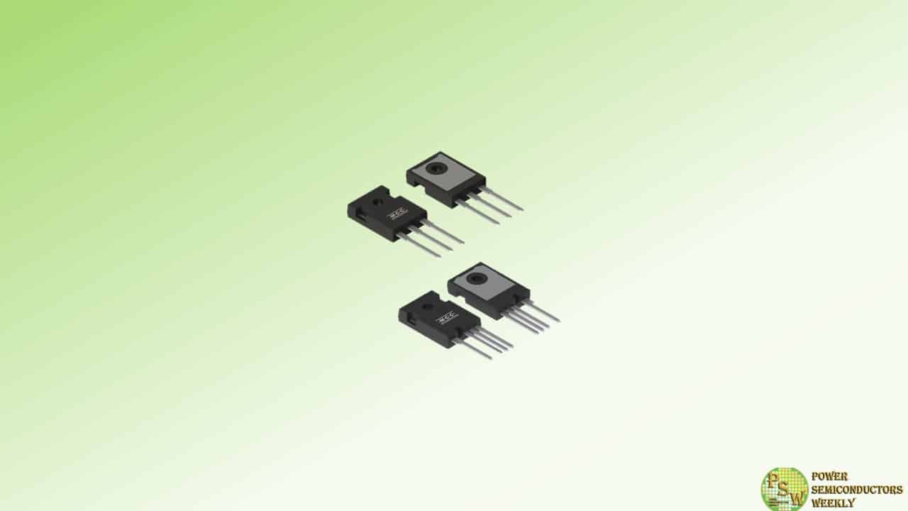
MCC Semi is expanding advanced silicon carbide portfolio with six new 650V SiC MOSFETs. Designed for demanding applications, these components boast high-voltage capability and an on-resistance range of 25 mΩ to 100 mΩ. They’re also equipped with avalanche ruggedness, low switching losses, and enable high-speed switching with a low gate charge.
Their efficiency-boosting design and TO247 package deliver superior thermal performance, while the 3-pin or 4-pin (Kelvin-source pin) options enhance their versatility. These new MOSFETs minimize losses without compromising power handling, making them an intelligent choice for various industrial and telecommunications systems.
Features & Benefits:
- High switching speed with low gate charge
- Low switching losses
- Wide on-resistance selection ranging from 25 mΩ to 100 mΩ
- Avalanche ruggedness for enhanced durability
- TO247 3-pin and 4-pin package options
- Kelvin-source connection for precision (4-pin only)
Original – Micro Commercial Components
-
DCDC converters are essential in any electric or hybrid vehicle to connect the high-voltage battery to the low-voltage auxiliary circuits. This includes 12 V power headlights, interior lights, wiper and window motors, fans, and at 48 V, pumps, steering drives, lighting systems, electrical heaters, and air conditioning compressors. In addition, the DCDC converter is important for developing more affordable and energy-efficient vehicles with an increasing number of low voltage functions.
According to TechInsights, the global automotive DC-DC converter market size was valued at USD 4 billion in 2023 and is projected to grow to USD 11 billion by 2030, exhibiting a CAGR of 15 percent during the forecast period. Gallium nitride (GaN) in particular plays a crucial role here, as it can be used to improve the power density in DCDC converters and on-board chargers (OBC).
For this reason, Vitesco Technologies, a leading supplier of modern drive technologies and electrification solutions, has selected GaN to improve the power efficiency of its Gen5+ GaN Air DCDC converter. The CoolGaN™ Transistors 650 V from Infineon Technologies AG significantly improve the overall system performance while minimizing system cost and increasing ease of use. As a result, Vitesco created a new generation of DCDC converters that set new standards in power density (efficiency of over 96%) and sustainability for power grids, power supplies, and OBCs.
The advantages of GaN-based transistors in high-frequency switching applications are considerable, but even more important is the high switching speed, which has been increased from 100 kHz to over 250 kHz. This enables very low switching losses, even in hard-switched half-bridges, with minimized thermal and overall system losses.
In addition, Infineon’s CoolGaN Transistors feature high turn-on and turn-off speeds and are housed in a top-cooled TOLT package. They are air-cooled, eliminating the need for liquid cooling and thereby reducing overall system costs. The 650 V devices also improve power efficiency and density, enabling an output of 800 V. In addition, they feature an ON-resistance (R DS(on)) of 50 mΩ, a transient drain-to-source voltage of 850 V, an I DS,max of 30 A, and an I DSmax,pulse of 60 A.
“We are delighted to see industry leaders like Vitesco Technologies using our GaN devices and innovating with their applications,” said Johannes Schoiswohl, Senior Vice President & General Manager, GaN Systems Business Line Head at Infineon. “The ultimate value of GaN is demonstrated when it changes paradigms, as in this example of moving from a liquid-cooled system to an air-cooled system.”
With GaN Transistors, Vitesco Technologies was able to design its Gen5+ GaN Air DCDC converters with passive cooling, which reduces the system’s overall cost. The GaN devices also allow for simplified converter design and mechanical integration. As a result, the DCDC converters can be flexibly positioned in the vehicle, reducing the workload for manufacturers.
The use of GaN also allows the power of the converters to be scaled up to 3.6 kW and the power density to be increased to over 4.2 kW/l. The Gen5+ GaN Air DCDC converters offer an efficiency of over 96 percent and improved thermal behavior compared to the Gen5 Liquid-Cooled converters. They provide a two-phase output of 248 A at 14.5 V continuous.
The phases can be combined to achieve the maximum output power. Still, it is also possible to switch off one phase under partial load conditions and interleave the switching frequency between the two phases. In addition, by switching the input of two phases in series, the converters based on the CoolGaN power transistors 650 V can be used to implement 800 V architectures without exceeding the maximum blocking voltage of the device. The converters also feature an isolated half-bridge topology consisting of a GaN-based half-bridge, a fully isolated transformer, and an active rectifier unit for each phase.
Original – Infineon Technologies
-

As global decarbonization efforts drive demand for power semiconductors, Infineon Technologies AG has officially opened the first phase of a new fab in Malaysia that will become the world’s largest and most competitive 200-millimeter silicon carbide (SiC) power semiconductor fab. Malaysian Prime Minister YAB Dato’ Seri Anwar Ibrahim and Chief Minister of the state of Kedah YAB Dato’ Seri Haji Muhammad Sanusi Haji Mohd Nor joined Infineon CEO Jochen Hanebeck, to symbolically launch production.
The highly efficient 200-millimeter SiC power fab will strengthen Infineon’s role as the global leader in power semiconductors. The first phase of the fab, with an investment volume of two billion euros, will focus on the production of silicon carbide power semiconductors and will include gallium nitride (GaN) epitaxy. SiC semiconductors have revolutionized high-power applications because they switch electricity even more efficiently and enable even smaller designs.
SiC semiconductors increase efficiency in electric vehicles, fast charging stations and trains as well as renewable energy systems and AI data centers. 900 high-value jobs will be created already in the first phase. The second phase, with an investment of up to five billion euros, will create the world’s largest and most efficient 200-millimeter SiC power fab. Overall, up to 4.000 jobs will be created with the project.
“New generations of power semiconductors based on innovative technology such as silicon carbide are an absolute prerequisite to achieving decarbonization and climate protection. Our technology increases the energy efficiency of ubiquitous applications such as electric cars, solar and wind power systems and AI data centers. We are therefore investing in the largest and most efficient high-tech SiC production facility in Malaysia, backed by strong customer commitments,” said Jochen Hanebeck, CEO of Infineon Technologies AG. “Since the demand for semiconductors will constantly rise, the investment in Kulim is highly attractive to our customers, who are backing it with their prepayments. It also increases the resilience of the supply chain for critical components needed for the green transition.”
“Infineon’s remarkable project reinforces Malaysia’s position as a rising major global semiconductor hub” says Malaysian Prime Minister YAB Dato’ Seri Anwar Ibrahim. “This major investment, which will locate the world’s largest and most competitive SiC power fab on our shores, will create jobs and opportunities, as well as attract suppliers, universities and top talent. Moreover, it will support Malaysia’s efforts to protect our climate by boosting electrification and increasing the efficiency of many applications, including electric cars and renewable energy. Thus, technology made in Malaysia will become a central part of global decarbonization efforts in the future.”
“Infineon’s deeply rooted presence in Kulim is a testament to the region’s potential as a hub for high-tech industries,” says Kedah Chief Minister YAB Muhammad Sanusi Md Nor. “This investment will not only create high-value job opportunities for the local community, it will also catalyze economic growth in the region. We are committed to continue providing top business conditions in Kedah and supporting Infineon’s efforts to establish a leading semiconductor facility in Kulim, which will have a positive ripple effect on the entire ecosystem.”
Infineon has secured design wins with a total value of approximately five billion euros and has received approximately one billion euros in prepayments from existing and new customers for the ongoing expansion of the Kulim 3 fab. Notably, these design wins include six OEMs in the automotive sector as well as customers in the renewable energy and industrial segments.
Kulim 3 will be closely connected to the Infineon site in Villach, Austria, Infineon’s global competence center for power semiconductors. Infineon already increased capacity for SiC and GaN power semiconductors in Villach in 2023. As “One Virtual Fab” for wide-bandgap technologies, both manufacturing sites now share technologies and processes which allow for fast ramping and smooth and highly efficient operation. The project also offers a high grade of resilience and flexibility, which will ultimately benefit Infineon’s customers.
The expansion will benefit from the excellent economies of scale already achieved for 200-millimeter manufacturing in Kulim. It will complement Infineon’s leading position in silicon, based on 300-millimeter manufacturing in Villach and Dresden. Thus, Infineon is strengthening its technological leadership across the entire spectrum of power semiconductors, in silicon as well as SiC and GaN.
In addition, the investment in wide-bandgap capacity in Kulim strengthens the local ecosystem and proves that Infineon is a reliable partner within the growing semiconductor hub Malaysia. Infineon’s operations in Malaysia started as early as 1973 in Melaka. In 2006, the company opened Asia’s first frontend fab in Kulim. Currently, Infineon employs more than 16.000 highly skilled people in Malaysia.
The Kulim 3 fab will be powered by 100% green electricity and will employ the latest energy efficiency measures to support Infineon’s goal of carbon neutrality. To avoid emissions, Infineon will use a state-of-the-art abatement system and green refrigerants that combine high efficiency with extremely low global warming potential. Other measures to ensure sustainable operations include state-of-the-art recycling of indirect materials and state-of-the-art water efficiency and recycling processes. Infineon is working towards recognition with the renowned Green Building Index certification.
Original – Infineon Technologies
-

Solitron Devices released the SD11740 , 1200V Silicon Carbide (SiC), low RDS(on) MOSFET.
Complimenting a strong offering of high voltage MOSFETs for high reliability/military applications Solitron is expanding its silicon carbide product offering for demanding commercial and industrial applications. Packaged in a SOT-227 the SD11740 offers ultra-low RDS(on) of 8.6mΩ.
The addition of the SOT-227 style package enables higher power applications for Solitron’s SiC based products in EV, power controllers, motor drive, induction heating, solid state circuit breakers and high voltage power supplies. The SD11740 offers 120A of continuous drain current. The SOT-227 features 3kV isolation to a copper heat sink base for outstanding low thermal impedance. The device provides a real Kelvin gate connection for optimal gate control. Either emitter terminal can be used as main or Kelvin emitter.
Designed for use as a power semiconductor switch the SD11740 outperforms silicon based MOSFETs and IGBTs. The standard gate drive characteristics allow for a true drop-in replacement to silicon IGBTS and MOSFETs with far superior performance. Ultra-low gate charge and exceptional reverse recovery characteristics, make them ideal for switching inductive loads and any application requiring standard gate drive.
Original – Solitron Devices
-

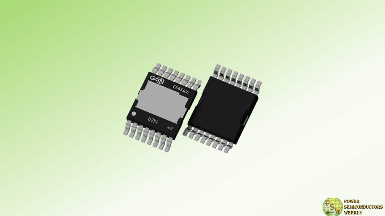
Navitas Semiconductor announced that Samsung had expanded adoption of Navitas’ GaNFast ICs from the original flagship Galaxy S22, S23 and S24 to the mainstream Galaxy A, and revolutionary Galaxy Z Fold6 and Galaxy Z Flip6 smartphones with enhanced Galaxy AI features.
GaN runs up to 20x faster than legacy silicon and enables chargers up to 3x more power and 3x faster charging in half size and weight. GaNFast power ICs enable high-frequency, high-efficiency power conversion, achieving up to a 50% shrink vs. prior designs.
The new 25W charger (EP-T2510) features new energy-saving technology to reduce standby losses by 75% to only 5 mW, which aligns with Navitas’ environmental advances, where every GaNFast IC saves 4 kg of CO2 vs. legacy silicon chips.
“Since enabling the world’s first production GaN charger in 2018, Navitas has pioneered and leads the adoption of GaN to replace legacy silicon chips,” noted David Carroll, Sr. VP Worldwide Sales for Navitas. “Our production partnership with Samsung dates back to the Galaxy S22 Ultra, and today’s announcement reflects the dramatic expansion of GaN from niche, flagship designs to adoption in high-volume, mainstream phones.”
Original – Navitas Semiconductor
-
Many different trends are taking center stage in both consumer electronics and industrial applications, such as portability, electrification, and weight reduction. All of these trends require compact and efficient designs. They also go hand in hand with unconventional PCB designs with severe space constraints that limit the use of external components.
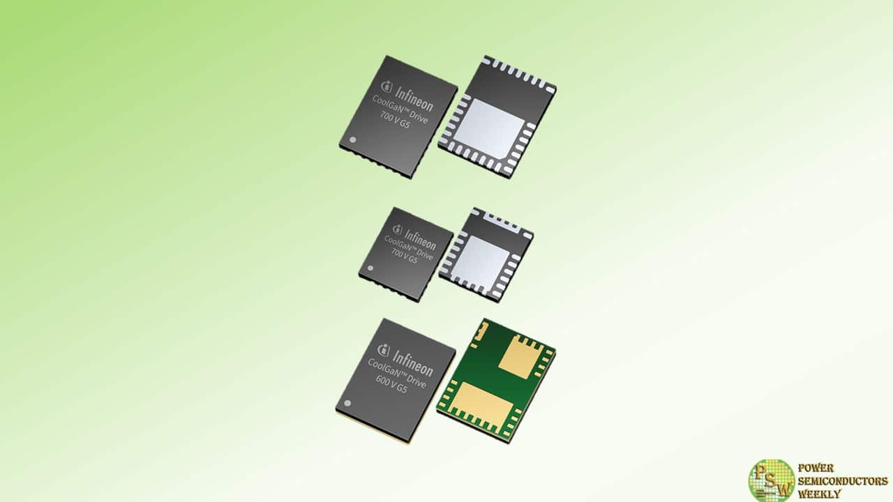
To address these challenges, Infineon Technologies AG expands its GaN portfolio with the CoolGaN™ Drive product family. It consists of the CoolGaN Drive 700 V G5 single switches, integrating one transistor plus gate driver in PQFN 5×6 and PQFN 6×8 packages, as well as the CoolGaN Drive HB 600 V G5 devices, combining two transistors with integrated high- and low-side gate drivers in a LGA 6×8 package. The new product family enables improved efficiency, reduced system size, and overall cost savings. This makes the devices suitable for longer-range e-bikes, portable power tools, and lighter-weight household appliances such as vacuums, fans, and hairdryers.
“For several years, Infineon has been focused on accelerating innovation in GaN to provide targeted solutions for real-world power challenges”, said Johannes Schoiswohl, Senior Vice President & General Manager, GaN Systems Business Line Head at Infineon. “The new CoolGaN Drive product family is another proof point of how we support our customers in developing compact designs with high power density and efficiency through GaN.”
The CoolGaN Drive family offers a wide range of single switches and half bridges with integrated drivers based on the recently announced CoolGaN Transistors 650 V G5. Depending on the product group, the components feature a bootstrap diode and are characterized by loss-free current measurement, and adjustable switch-on and switch-off dV/dt. They also provide OCP/OTP/SCP protection functions. As a result, the devices enable higher switching frequencies, leading to smaller and more efficient system solutions with high power density. At the same time, the bill of materials (BoM) is reduced. This not only results in a lower system weight, but also reduces the carbon footprint.
Samples of the half-bridge solutions are available now. Single-switch samples will be available starting Q4 2024. Further information is available at www.infineon.com/GaN-innovations.
Original – Infineon Technologies
-

Navitas Semiconductor extended its new portfolio of Gen-3 ‘Fast’ (G3F) 650 V SiC MOSFETs into a thermally-enhanced, rugged, high-speed, surface-mount TOLL (Transistor Outline Leadless) package designed for demanding, high-power, high-reliability applications.
Combining high-power capability and best-in-class low on-resistance of 20 to 55 mΩ, these 650 V SiC MOSFETs have been optimized for the fastest switching speed, highest efficiency, and increased power density demanded by applications such as AI data center power supplies, EV charging and energy storage and solar solutions (ESS).
Navitas’ GeneSiC products use a proprietary ‘trench-assisted planar’ technology that provides world-leading efficiency performance over the temperature range, with G3F MOSFETs delivering high-speed, cool-running performance that ensures up to 25°C lower case temperatures and up to 3x longer life than alternative SiC products.
Navitas’ latest 4.5 kW AI power system reference design features the G3F45MT60L (650V 40 mΩ, TOLL) G3F SiC MOSFET in an interleaved CCM-TP PFC topology. Complemented by the NV6515 (650V, 35mΩ, TOLL) GaNSafe™ Power IC in the LLC stage, the 4.5 kW solution has a peak efficiency above 97% and, at 137 W/inch3, it is the world’s highest power density AI PSU. For 400 V-rated EV battery systems, G3F in TOLL is an ideal technology for on-board chargers (OBC), DC-DC converters, and traction drives ranging from 6.6 to 22 kW.
The surface-mount TOLL package offers a 9% reduction in junction-to-case thermal resistance (RTH,J-C), 30% smaller PCB footprint, 50% lower height, and 60% smaller size than the traditional D2PAK-7L, enabling highest-power-density solutions, as demonstrated in the 4.5 kW AI solution. Additionally, with a minimal package inductance of only 2 nH, excellent fast-switching performance and lowest dynamic losses are achieved.
The G3F family in TOLL package is released and available for purchase.
Original – Navitas Semiconductor
-

VisIC Technologies Ltd. has partnered with Heraeus Electronics and PINK to develop an advanced power module utilizing D3GaN technology. This groundbreaking power module is based on a silicon nitride (Si₃N₄) ceramic substrate, an innovative silver (Ag) sintering process and advanced top side interconnect, promising unprecedented reliability and performance for battery electric vehicles (BEVs).
The collaboration brings together VisIC’s expertise in GaN-based devices, Heraeus Electronics’ cutting-edge packaging materials know-how, and PINK’s state-of-the-art sintering technology. The synergy of these industry leaders has culminated in the development of a power module that is setting new standards for GaN based power modules to revolutionize the EV industry.
VisIC’s D3GaN technology is at the heart of this power module, offering significant improvements in efficiency, thermal management, and power density. This technology leverages the superior electrical properties of gallium nitride to deliver faster switching speeds and higher power handling capabilities compared to traditional silicon-based devices.
The use of a Si₃N₄ metal ceramic substrate is a key innovation in this power module. Si₃N₄ is known for its excellent thermal conductivity, mechanical strength, and reliability under high-temperature conditions. These properties are crucial for the demanding environment of electric vehicle applications, ensuring the power module can withstand the rigors of everyday use while maintaining optimal performance.
The adoption of the silver sintering process by PINK enhances the thermal and electrical conductivity of the module. Silver sintering is a low-temperature bonding process that creates robust and reliable connections between components, improving the module’s overall durability and efficiency. This process is critical for the high reliability required in EV powertrains, where consistent performance is non-negotiable.
The resulting power module is designed to meet the stringent reliability and performance standards of the electric vehicle industry. Its advanced materials and innovative construction techniques ensure it can deliver the high-power density of over 500Arms/650V and efficiency needed for modern BEVs, while also offering long-term reliability and durability at a cost point near silicon devices.
This collaboration marks a significant milestone in the advancement of power electronics for electric vehicles. The integration of VisIC’s D3GaN technology with Heraeus Electronics’ sintering paste and PINK’s Ag and Cu sintering process and flexible sintering equipment sets a new benchmark for power module performance in the EV market. This innovation is expected to drive the adoption of GaN technology in EV applications, paving the way for more efficient, reliable, and sustainable electric transportation solutions.
Tamara Baksht, CEO of VisIC, state: “We are thrilled to work with the leading manufacturer of sintering processes of Heraeus Electronics and PINK and adapt their experience into GaN based power modules to develop the next generation of power module for high volume automotive inverter applications.”
PINK, Andrea Pink, CEO of PINK statement: “We are excited to work with such a future driven company as VisIC together with our long-term partner Heraeus Electronics, supporting the newest product innovation for GaN applications.”
Heraeus Electronics Dr. Michael Jörger, EVP Head of Business Line Power Electronic Materials added: “With our materials, application know-how and engineering services we are glad to work with our partners on speeding up the innovative approach of highly efficient GaN modules for automotive applications.”
Original – VisIC Technologies
-

Toshiba Electronic Devices & Storage Corporation and Toshiba Corporation (Toshiba Group) have developed technology that mitigates the parasitic oscillation that occurs during switching operations by power modules with silicon carbide (SiC) MOSFETs connected in parallel, even with a 60% smaller gate resistance than is typical. The technology reduces power loss in power modules, mitigates oscillation, and realizes highly reliable switching operations.
The drive for carbon neutrality is stimulating demand for technologies that improve energy efficiency in many areas, including renewables, railways, and industrial equipment. In these sectors, the application of power modules built around SiC MOSFETs is seen as a solution that supports high-speed switching at high voltages and large currents—which is particularly important for the miniaturization of power converters, where higher switching frequencies result in higher rates of switching losses against power consumption.
Connecting multiple chips in parallel in power modules can form oscillation circuits, the result of wiring inductance between the chips and their parasitic capacitance. It can reduce module reliability if not countered, which is usually done by increasing gate resistance. However, this approach slows switching speed, resulting in a trade-off with switching losses. For power modules with SiC MOSFETs to perform high-speed switching, another approach is needed.
Toshiba Group used an equivalent circuit model of the power module (Figure 1) to determine the theoretical condition that triggers parasitic oscillation, and developed a wiring layout less likely to cause it. This was done by analyzing simulations of parasitic oscillation occurs when Lg/Ls, the ratio of gate-to-gate inductance Lg and source-to-source inductance Ls of parallel chips, is below a certain value (Figure 2). As increasing Lg/Ls is an effective means of mitigating parasitic oscillation, Toshiba Group fabricated prototype modules with different Lg/Ls and measured switching. This confirmed that increasing Lg/Ls mitigated oscillation, even with a 60% smaller gate resistance than that required by the alternative approach of increasing gate resistance (Figure 3).
Applying this approach to oscillation mitigation in power modules now under development has realized a power module less likely to cause parasitic oscillation, even with minimal gate resistance, that achieves low power loss with mitigated oscillation, and delivers highly reliable switching operation. Toshiba Group will continue to make refine the modules toward an early product launch.
Toshiba Group presented the details of this technology on June 6 at the 36th International Symposium on Power Semiconductor Devices and ICs (ISPSD) 2024, an international power semiconductor conference held in Bremen, Germany from June 2 to 6.
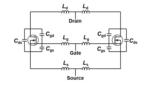
Figure 1. Model equivalent circuit of two MOSFETs connected in parallel 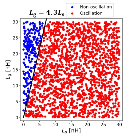
Figure 2. Simulation of oscillation in two MOSFETs with zero gate resistance connected in parallel 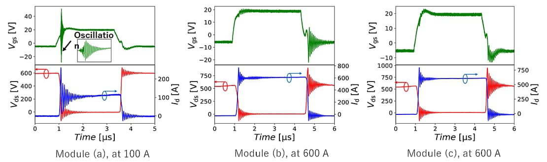
Vgs: Gate-Source voltage, Vds: Drain-Source voltage, Id: Drain current
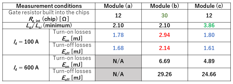
Figure 3. Switching waveforms and switching losses of the prototype modules (Source: Toshiba Group tests) Original – Toshiba
-

MCC introduced the latest additions to its robust portfolio: 10 1200V SiC N-channel MOSFETs in versatile TO-247-4, TO-247-4L, and TO-247AB packages. These new MOSFETs are available in 3-pin and 4-in (Kelvin source) configurations and meet the rising demand for high-power, high-voltage applications.
Boasting exceptional on-resistance values from 21mΩ to 120mΩ (typ.) and fast switching speeds, these components are the ones you can count on for reliable performance. Their excellent thermal properties and fast intrinsic body diode ensure smooth, efficient operation in the most challenging conditions, making them a must-have for critical power systems.
Features & Benefits:
- High-power capability: 1200V MOSFET with SiC technology
- Fast, reliable switching: Intrinsic body diode improves efficiency & ruggedness Enhanced performance: High switching speed with low gate charge
- Wide on-resistance selection: ranging from 21mΩ to 120mΩ (typ.)
- Efficiency: Superior thermal properties and low switching losses
- Durability: Avalanche ruggedness
- Versatility: TO247 3-pin and 4-pin package options
Original – Micro Commercial Components
