-
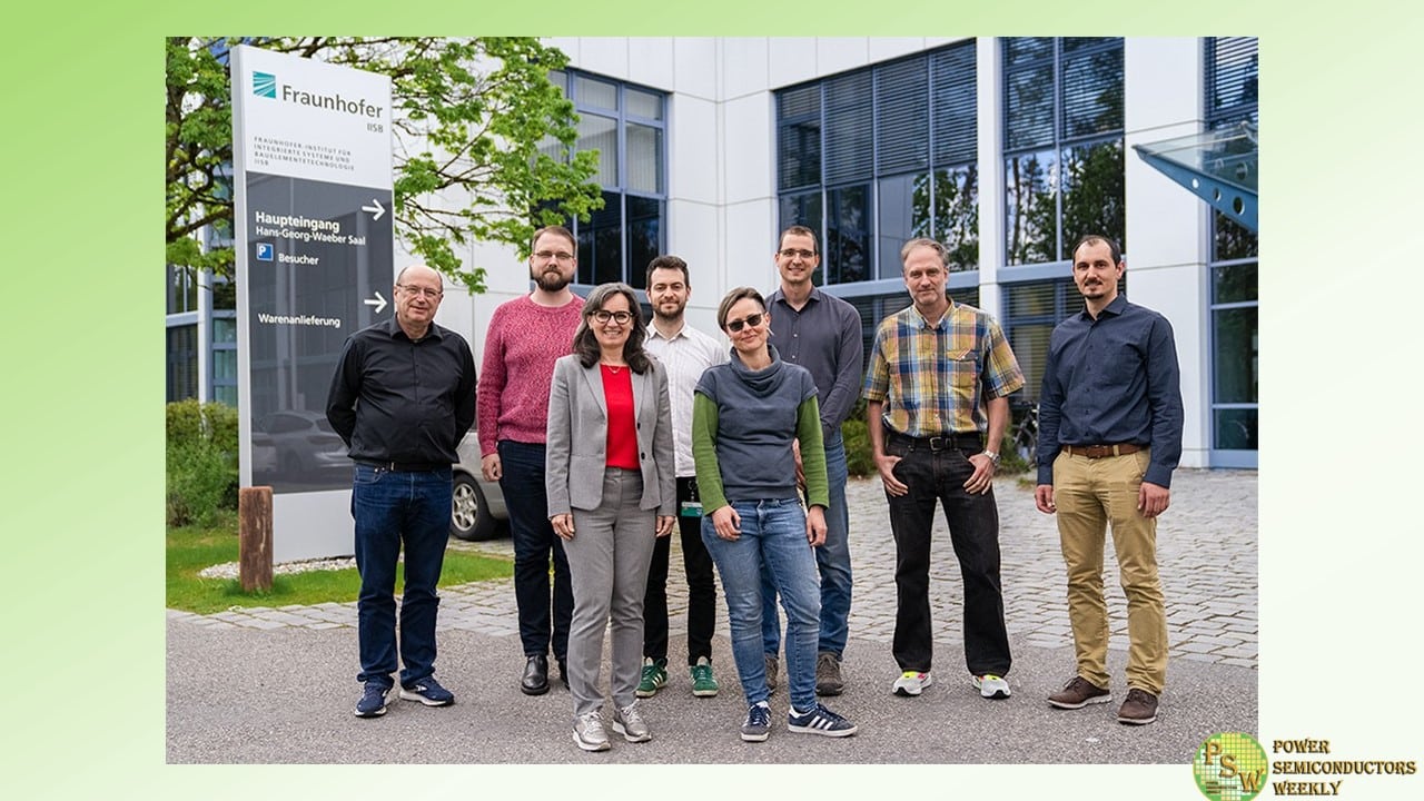
Semilab Zrt. and Fraunhofer IISB announced the official kick-off of their strategic partnership.
Within their new joint lab, located at the IISB in Erlangen, the partners develop state-of-the-art metrology and inspection solutions for (ultra-) wide-bandgap semiconductor materials.
The goal is to take semiconductor metrology to a next level along the value chain, from base material to die. By bringing new features and tools from lab to market, new standards for SiC, GaN and other (U)WBG semiconductors will be set.Original – Fraunhofer IISB
-

Navitas Semiconductor announced that Virtual Forest, one of India’s leading electronics design companies specializing in motor control and human interface technologies for consumer appliances, fluid movement and mobility, has adopted its GaNFast™ power integrated circuits (IC) technology for a zero-emission, powerful 3 hp (2,250W) solar-powered irrigation pump.
For many farmers worldwide, irrigating remote crops requires powerful pumps to lift water from rivers and streams up to field-level, with the majority powered by polluting and noisy diesel generators or expensive, lossy long-distance electrical cables. The Virtual Forest solar pump with maximum power point tracking (MPPT) operates in conjunction with solar panel and energy storage to provide robust, energy-independent and pollution-free performance at the point of use.
The 3 hp (2,250W) pump is remotely accessed via quad-band IoT with low power consumption. It can raise over 50 gallons-per-minute of water to a height of over 90 feet, enough to water 3 acres of farmland, and help to produce 10 tonnes of wheat. Further, the IoT enabled solar pump ensures optimal water usage through intelligent analytics, therefore minimizing ground water utilization.
Navitas GaNSense™ half-bridge power ICs monolithically by integrating two GaN power FETs with GaN drivers, level-shifters, protection features and high-efficiency loss-less current sensing. High-efficiency NV6269 half-bridge ICs, in easy-to-use 8×10 mm QFN packages are used in a 3-phase motor inverter, with 3x-5x energy savings vs legacy silicon IGBTs.
“The $450 million solar-pump market in India is expected to reach $1.5 Bn by 2026, calling for a solar revolution on Indian fields,” said Virtual Forest’s CEO, Omer Basith, adding “Reliable, off-grid systems are critical to overcome food insecurity and achieve energy efficiency. Leveraging Navitas’ high-power, efficient GaNSense™ half-bridge, we seek to deliver a robust solution to the market. We are nurturing our dream to drive gigatons of reduction in carbon emissions, thereby making the world a greener place to live in. Hence, our name — Virtual Forest.”
“The design team at Virtual Forest adopted the GaNSense half-bridges very quickly, for a fast time-to-market,” said Alessandro Squeri, Navitas’ Senior Sales Director. “With GaNSense, ‘easy-to-use feature, Virtual Forest comes into the partnership with high efficiency, low component count and a robust design for tough environments.”
Original – Navitas Semiconductor
-

Infineon Technologies AG supplies its power semiconductor devices to FOXESS, a fast-growing leader in the green energy industry and a manufacturer of inverters and energy storage systems. The two sides aim at promoting the development of green energy.
Infineon will provide FOXESS with its CoolSiC™ MOSFETs 1200 V, which will be used with EiceDRIVER™ gate drivers for industrial energy storage applications. At the same time, FOXESS’ string PV inverters will use Infineon’s IGBT7 H7 1200 V power semiconductor devices.
The global market for photovoltaic energy storage systems (PV-ES) has grown at a high speed in the last years. As competition in the PV-ES market accelerates, improving power density has become key to success, and how to improve efficiency and power density for energy storage applications has attracted much attention. Infineon’s CoolSiC MOSFET 1200 V and IGBT7 H7 1200 V series power semiconductor devices adopt the latest semiconductor technologies and design concepts that are tailored to industrial applications.
Mr. Yu Daihui, Senior Vice President and Head of Industrial & Infrastructure of Infineon Technologies Greater China said, “As an industry leader in power semiconductors, we are proud to work closely with FOXESS. We will continue to drive decarbonization by enabling higher power density and more reliable systems for PV-ES applications.”
Mr. Zhu Jingcheng, Chairman of FOXESS, said, “Thanks to the support of Infineon’s advanced components, FOXESS’ products have been significantly improved in terms of reliability and efficiency. This has been an important driving force for FOXESS’ growth. Infineon’s technical support and product quality have not only strengthened our competitiveness, but also expanded our presence in the market. We are confident about the future and look forward to further cooperation with Infineon to jointly promote the development of the industry and create greater value for our customers.”
With a high power density, Infineon’s CoolSiC MOSFETs 1200 V can reduce losses by 50 percent and provide ~2 percent additional energy without increasing the battery size, which is especially beneficial for high-performance, lightweight, and compact energy storage solutions. FOXESS’ H3PRO 15 kW-30 kW energy storage series uses Infineon’s CoolSiC MOSFETs 1200 V for all models. Thanks to Infineon’s excellent performance, the H3PRO series has achieved an efficiency of up to 98.1 percent and excellent EMC performance; with superior performance and reliability, the H3PRO series has seen rapid sales growth in the global market.
Infineon’s TRENCHSTOP IGBT7 H7 650 V / 1200 V series has lower losses and helps improve the overall efficiency and power density of inverters. In high-power inverter projects, high-current mold packaged discrete devices with current handling capability above 100 A can reduce the number of IGBTs in parallel and replace the IGBT module solution, further improving system reliability and reducing costs; in addition, the H7 series has become an industry benchmark for its high-quality performance and greater resistance to humidity.
At present, FOXESS’ main industrial and commercial model, the R Series 75-110 kW, redefines the overall design of the 100 kW model by using IGBT7 H7 series discretes, and the efficiency of the whole machine can reach up to 98.6 percent. Thanks to the low power loss and high power density of the IGBT7 H7 series in discrete packages, technical problems such as current sharing in the paralleling process can be simplified and optimized.
Every power device needs a driver, and the right driver can make the design a lot easier. Infineon offers more than 500 EiceDRIVER gate drivers with typical output currents of 0.1 A~18 A and comprehensive protection functions including fast short-circuit protection (DESAT), active Miller clamp, shoot-through protection, fault reporting, shutdown, and overcurrent protection, suitable for all power devices including CoolSiC and IGBTs.
Original – Infineon Technologies
-

Axcelis Technologies, Inc. arranged multiple shipments of the Purion Power Series™ ion implanter systems to leading silicon carbide (SiC) power device chipmakers worldwide. The shipments, all shipped in the first quarter, included the Purion H200™ SiC high current, the Purion XE™ SiC high energy and the Purion M™ SiC medium current implanters.
The 150mm and 200mm systems will be used in high volume production of power devices supporting automotive, industrial, energy, and other power intensive applications.
President and CEO Russell Low commented, “We continue to win new customers and expand our footprint at existing customers globally. The Purion Power Series is the market leader due to its highly differentiated features and process control capabilities that are enabling for power device applications. Axcelis is the only ion implant company that can deliver complete recipe coverage for all power device applications.”
Original – Axcelis Technologies
-
Chicony Power Technology, a worldwide leading manufacturer of power supplies and a pioneer in power electronics, has announced the winners of its Annual Partner Awards, honoring Infineon Technologies AG as its 2023 “GaN Strategic Partner of the Year”.
Infineon has been recognized by Chicony Power as its top partner for gallium nitride (GaN)-based power supplies, including notebook adapters, as well as ICT applications in gaming, storage and servers. This acknowledgment is the result of Infineon’s high standards for product selection, application expertise, high reliability and cost-effectiveness.
GaN stands out as one of the most crucial technologies which are essential for improving the efficiency of power supplies and reducing their product size. Pooling Infineon’s leading GaN expertise and Chicony Power’s remarkable capabilities in power supply system design, the win-win collaboration has helped push the boundaries of innovation and further strengthened both companies’ leading positions in energy-efficient power solutions. As of today, the GaN adoption rate in Chicony Power’s high-watt adapters has reached 20 percent, and this rate is rapidly increasing.
“Unrivalled R&D resources, a comprehensive application understanding and a large number of customer projects let Infineon continuously drive its roadmap for becoming a leading GaN Powerhouse,” said Adam White, Division President Power & Sensor Systems at Infineon Technologies. “The Strategic Partner of the Year award from Chicony Power is a great honor for us. We see this as part of our common mission to drive decarbonization and digitalization together.”
“We’re pleased to honor Infineon, which has played a pivotal role in driving customer success throughout 2023, as our GaN Strategic Partner of the Year,” said Peter Tseng, President of Chicony Power Technology. “Our Vision is to be a global pioneer in the implementation of new technology that enhances power supply efficiency, reduces the carbon footprint of power supplies and helps create a greener world. We would like our Annual Partner Awards to encourage Infineon and all other partners to maintain the momentum in jointly promoting GaN technology in the market alongside Chicony Power, making the power industry greener and cleaner.”
Original – Infineon Technologies
-
Coherent Corp. announced that it secured $15 million in funding from the Creating Helpful Incentives to Produce Semiconductors (CHIPS) and Science Act of 2022 that provided the Department of Defense (DoD) with $2 billion to strengthen and revitalize the U.S. semiconductor supply chain.
One of the key objectives of the CHIPS program is to nurture ecosystems that reduce risk, incentivizing large-scale private investment in production, breakthrough technologies, and workers. To that end, the DoD, through the Naval Surface Warfare Center Crane Division and the National Security Technology Accelerator, established eight Microelectronics Commons regional innovation hubs in September, including the Commercial Leap Ahead for Wide-Bandgap Semiconductors (CLAWS) Hub based in North Carolina and led by NC State University.
As a member of the CLAWS Hub, Coherent will receive $15 million to accelerate the commercialization of next-generation wide- and ultrawide-bandgap semiconductors, namely, silicon carbide and single-crystal diamond, respectively.
“We are excited to be recipients of funding from the CHIPS Act, delighted to be part of the CLAWS Hub, and proud to help the U.S. establish a strategic, long-term leadership position in these critical next-generation semiconductor technologies,” said Sohail Khan, Executive Vice President, Wide-Bandgap Electronics.
“Wide- and ultrawide-bandgap semiconductors enable the electrification of transportation, including road vehicles, high-speed trains, and mobile industrial machinery. They also enable smart power grids to efficiently respond to fluctuations in energy demands by regulating the delivery of electricity from conventional and renewable sources to distribution networks, as well as to and from utility-scale power storage and microgrids.”
In addition to DoD requirements for high-voltage, high-power applications and systems including hybrid electric vehicles (HEVs), more electric aircraft (MEA) components, directed energy, Navy vessel power systems, and all-electric ships, silicon carbide power electronics are increasingly recognized for their potential to greatly improve the energy efficiency of artificial intelligence (AI) data centers and traditional hyperscale data centers, where power consumption is growing rapidly due to the exploding demand for data- and compute-intensive workloads from AI, cryptocurrency mining, and blockchain applications.
Single-crystal diamond promises to exceed the performance of silicon carbide and greatly expand the applications universe with quantum computing, quantum encryption, and quantum sensing.
Original – Coherent
-
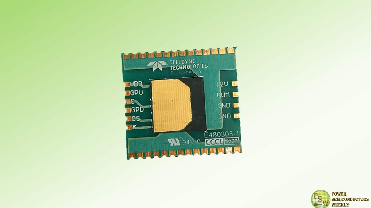
Teledyne e2v HiRel Electronics announced the release of the TDGM650LS60, the first product in its innovative new 650V power module family. This new module utilizes a Teledyne high voltage Gallium Nitride (GaN) transistor and integrates an isolated driver in one package.
Designed to serve as a load switch or solid-state switch, the TDGM650LS60 offers unparalleled performance and versatility. With the driver providing 5KV isolation and a GaN transistor boasting a minimum breakdown voltage of 650V, this module ensures robust and dependable operation in diverse environments.
One of the standout features of the TDGM650LS60 is its lightning-fast switching time coupled with the absence of moving parts. This unique combination not only enhances operational efficiency but also significantly elevates the reliability of the device. As a result, the TDGM650LS60 is ideally suited for high-reliability applications, including but not limited to Space, Avionics, and Military sectors.
“This launch marks a significant milestone in Teledyne’s commitment to innovation” said Mont Taylor, Vice President and Business Development Manager at Teledyne e2v HiRel. “The TDGM650LS60 represents the culmination of our dedication to pushing the boundaries of technology, offering our customers performance, reliability, and versatility in their applications.”
Original – Teledyne e2v HiRel Electronics
-

SemiQ has opened its newest office in Taiwan. This strategic move underscores SemiQ’s commitment to providing enhanced ground support to its valued customers in the region while further solidifying its presence in the Asia-Pacific market.
As a Product Engineering and Global Sourcing Center, the new office, located near the Taiwan High Speed Rail Hsinchu Station, will serve as a vital hub, facilitating seamless interfacing with key stakeholders including Hsinchu Foundry, Miaoli Test Facility, Far East OSATs, and Taiwan Sales Office.
“Expanding our presence in Taiwan represents a significant milestone for SemiQ as we continue to strengthen our global operations and better serve our customers,” said Michael Tsang, VP, Product Engineering and Operations at SemiQ. “The opening of this office underscores our dedication to providing unparalleled support and resources to our customer base in the region.”
Mr. Tsang, a seasoned professional with extensive experience in semiconductor industry dynamics, will lead the Taiwan office. His expertise will be instrumental in managing demand, fostering partnerships, and ensuring the highest level of service delivery to SemiQ’s customers.
The strategic location of the new office near key industry players and transportation hubs will enhance SemiQ’s ability to collaborate effectively with its partners, streamline operations and expedite response times to customer needs.
“We are excited about the opportunities that the Taiwan office brings in terms of strengthening relationships with our partners and better understanding the evolving needs of the market,” added Mr. Tsang. “This expansion aligns with our vision of driving innovation and delivering value-added solutions to our customers.”
Establishing the Taiwan office complements SemiQ’s existing wafer processing facilities in the region. It underscores its commitment to providing superior SiC solutions for ultra-efficient, high-performance, and high-voltage applications.
Original – SemiQ
-

Axcelis Technologies, Inc. announced a shipment of the Company’s Purion EXE™ SiC high energy implanter as well as a successful Purion H200™ SiC medium energy implanter evaluation closure at leading power device chipmakers located in Japan. The systems will be used for 150mm and 200mm production of silicon carbide power devices supporting automotive, industrial, energy, and other power intensive applications.
Greg Redinbo, Executive Vice President, Marketing and Applications remarked, “The successful evaluation closure of the 200mm Purion H200 SiC system enables it to join an existing 200mm Purion EXE SiC in production at a leading power device customer in Japan.” Dr. Redinbo continued, “The shipment of an additional Purion EXE SiC to a new 150mm customer in Japan highlights growing customer requirements for even higher energy ion implant recipes on advanced SiC power devices, which the Purion Power Series provides.”
President and CEO, Russell Low commented, “We look forward to supporting our growing installed base in Japan and remain focused on expanding our market share by providing customers with the most innovative implant technology and support solutions to ensure their success. The Purion Power Series is the market leader due to its highly differentiated features and process control capabilities that are enabling for power device applications. Axcelis is the only ion implant company that can deliver complete recipe coverage for all power device applications.”
Original – Axcelis Technologies
-

Aehr Test Systems announced it has received an initial customer order for a FOX-NP™ wafer level test and burn-in system, multiple WaferPak™ Contactors, and a FOX WaferPak Aligner to be used for engineering, qualification, and small lot production wafer level test and burn-in of their silicon carbide devices.
The customer is multiple billion dollar per year global semiconductor company with locations across Europe, Asia, and the Americas that serves various industries including automotive, industrial, mobile, and consumer applications. The FOX-NP system, including the FOX WaferPak Aligner and initial WaferPaks, are scheduled to ship over the next few months.
The FOX-NP system is configured with the new Bipolar Voltage Channel Module (BVCM) and Very High Voltage Channel Module (VHVCM) options that enable new advanced test and burn-in capabilities for silicon carbide power semiconductors using Aehr’s proprietary WaferPak full wafer Contactors.
Gayn Erickson, President and CEO of Aehr Test Systems, commented, “We are very excited that this new customer selected our FOX-P solution for engineering, qualification, and production of their silicon carbide power devices. After working with the Aehr team and our technology solutions over an extended period of time, they felt secure in our ability to aid them in achieving these goals. A key feature in their selection of our FOX solution is its proven ability to cost-effectively implement their target burn-in and stabilization requirements, including 100% traceability and proof that every device on the wafer is burned in for the needed test duration.
“This customer currently has a wide range of automotive products and is entering the silicon carbide market to address several applications that include automotive, industrial, and electrification infrastructure. Key capabilities of our solution include our ability to scale from engineering and qualification and small lot production with the FOX-NP system to large scale production with the FOX-XP with Automated WaferPak Aligner. They have told us that they plan to transition to our FOX-XP multi-wafer test and burn-in systems for high-volume production. Aehr’s FOX-P technology facilitates a seamless transition from engineering to high-volume production with 100% compatibility between systems.
“This customer sees the enormous opportunity for silicon carbide power devices in industrial and power applications. William Blair forecasts that in addition to the 4.5 million six-inch equivalent wafers that will be needed to meet the demand for electric vehicle related silicon carbide devices in 2030, another 2.8 million wafers are needed to address industrial, solar, electric trains, energy conversion and other applications in 2030. The cost of ownership of our solution proves to be more cost-effective and efficient for these devices than package part burn-in after the die are packaged. This is a strong testimony of the advantage of wafer level burn-in as a better alternative to package part burn-in.
“The FOX family of compatible systems including the FOX-NP and FOX-XP multi-wafer test and burn-in systems and Aehr’s proprietary WaferPak full wafer contactors provide a uniquely cost-effective solution for burning in multiple wafers of devices at a single time to remove early life failures of silicon carbide devices, which is critical to meeting the initial quality and long-term reliability of the automotive, industrial, and electrification infrastructure industry needs.”
The FOX-XP and FOX-NP systems, available with multiple WaferPak Contactors (full wafer test) or multiple DiePakTM Carriers (singulated die/module test) configurations, are capable of functional test and burn-in/cycling of devices such as silicon carbide and gallium nitride power semiconductors, silicon photonics as well as other optical devices, 2D and 3D sensors, flash memories, magnetic sensors, microcontrollers, and other leading-edge ICs in either wafer form factor, before they are assembled into single or multi-die stacked packages, or in singulated die or module form factor.
Original – Aehr Test Systems
