-
 LATEST NEWS / SiC / WBG
Axcelis Technologies to Deliver Purion M™ SiC Implanters to Several Power Device Chipmakers in China
March 20, 2024
2 Min ReadAxcelis Technologies, Inc. announced multiple shipments of the Company’s Purion M™ SiC medium current implanter to several leading power device chipmakers located in China. The systems, which shipped in the first quarter, will be used for 150mm production of silicon carbide power devices supporting automotive, industrial, energy, and other power intensive applications.
President and CEO, Russell Low commented, “We look forward to supporting our customers as they expand their manufacturing capabilities in this growing silicon carbide power device segment. To meet market demand, chipmakers need to maximize their yield and add capacity, while meeting a range of technical challenges unique to power devices. The Purion M SiC Power Series platform’s common and flexible architecture, coupled with its uniquely differentiated high temperature capability, makes it ideally suited for this expanding application.”
Executive Vice President of Marketing and Applications, Greg Redinbo added “The Purion M SiC tool provides customers an implanter with a broad dose and energy range perfect for the early phases of a fab production ramp. The Purion M SiC sets the stage for the future introduction of the Purion H200™ SiC and Purion XE™ SiC. Use of the full Purion Power Series family enables higher fab productivity, lower cost of ownership and the ability to manufacture more advanced silicon carbide power devices.”
Original – Axcelis Technologies
-
Recently the European Space Agency (ESA) started its search for the technological advantage to improve their systems. Lead by research fellow Dr. Antxon Arrizabalaga, the project is aimed at studying the latest semiconductor technologies and exploring the impact they can have in the future of the space industry.
During its research, Dr. Antxon Arrizabalaga is looking forward to answer the following questions:
- Which are the next system-level figures the space power industry wants to achieve?
- Can the wide bandgap semiconductors help to achieve these figures?
- Which semiconductor ratings are demanded by the space power industry for each application?
At the moment the research project lead by Dr. Arrizabalaga is focusing on the silicon carbide (SiC) power semiconductor devices, as they are better suited for the requirements of the high-power applications. The team has already had several meetings with the main European space power companies discussing the points of interest mentioned above.
As a result, ESA received rich feedback with industry requirements and new ideas. And as anticipated, most of the companies are looking to the ways to increase power of their systems.
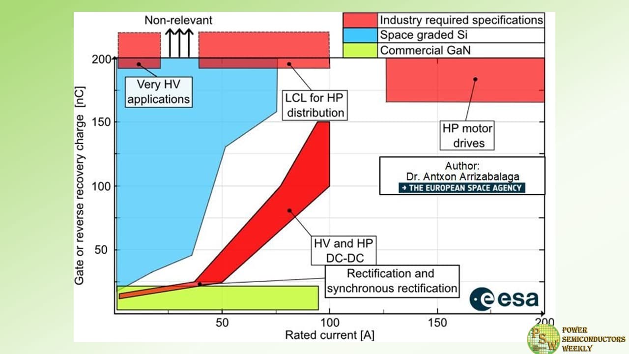
Thus, the following applications were mentioned the most:
- Latching current limiters (LCL) for high power distribution
- High-voltage (HV), increasing the traditional bus voltage, and high-power (HP) DC-DC converters
- Rectification and synchronous rectification
- HP motor drives
- Very HV applications, around and over 1 kV
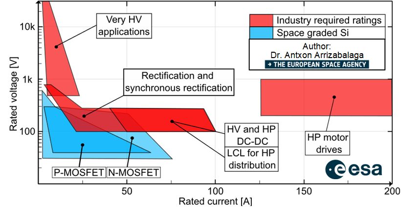
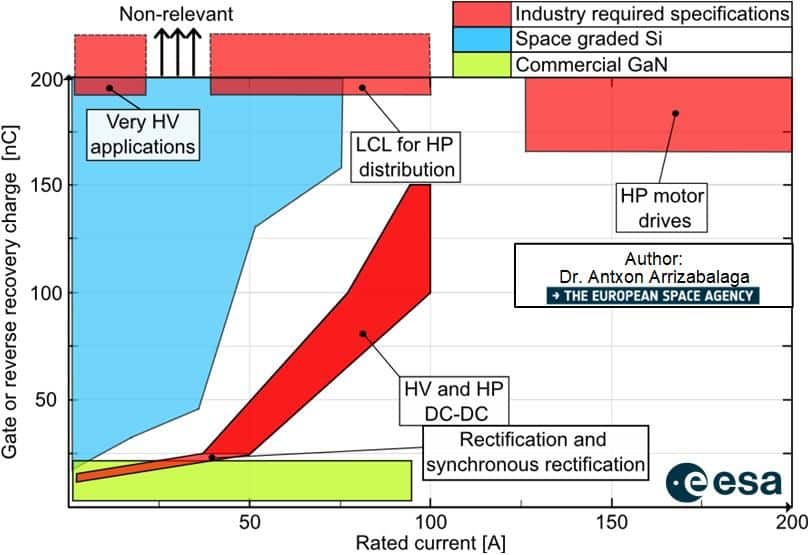
Figure 1. The ratings of the semiconductor devices required by the industry for each application
According to Dr. Arrizabalaga, ESA classifies innovations in three categories, according to the degree of innovation they bring when compared to the state-of-the-art:
- Enhancing. It brings a substantial improvement to the state-of-the-art system.
- Based on a technology replacement
- For SiC devices it means replacing the Si devices in an existing application and optimizing the system to get system-level benefits
- Low risk, development time and cost for manufacturers
- Straightforward adoption by industry and high probability of success
- Enabling. It will allow a new feature, new application, or even a new mission.
- Critical technologies for a certain feature, application or mission
- For SiC devices it means that without the adoption of such devices, the new desired feature, application or mission is no longer possible
- Medium-high risk for manufacturers, higher development cost and effort, since it has never been done before
- More challenging adoption by industry, and lower probability of success
- Game-changing. It promises to bring entirely new capabilities (not considered for this study).
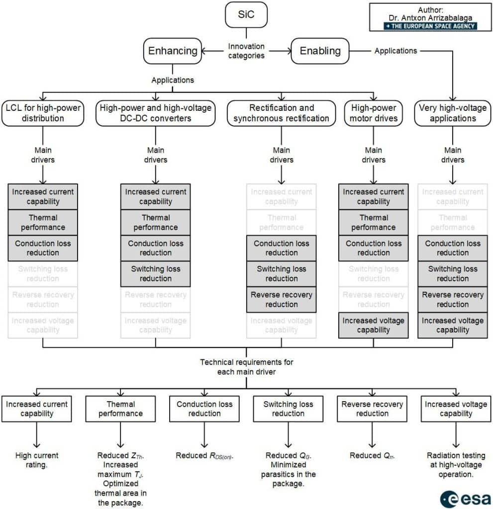
Figure 2. Classification of the applications mentioned by the industry and the main drivers needed to be optimized for each application.
The European Space Agency research team is looking forward to support the successful adoption of the wide bandgap (WBG) power semiconductor devices by the European space power industry, giving the European industry a competitive edge.
Original – Dr. Antxon Arrizabalaga
-
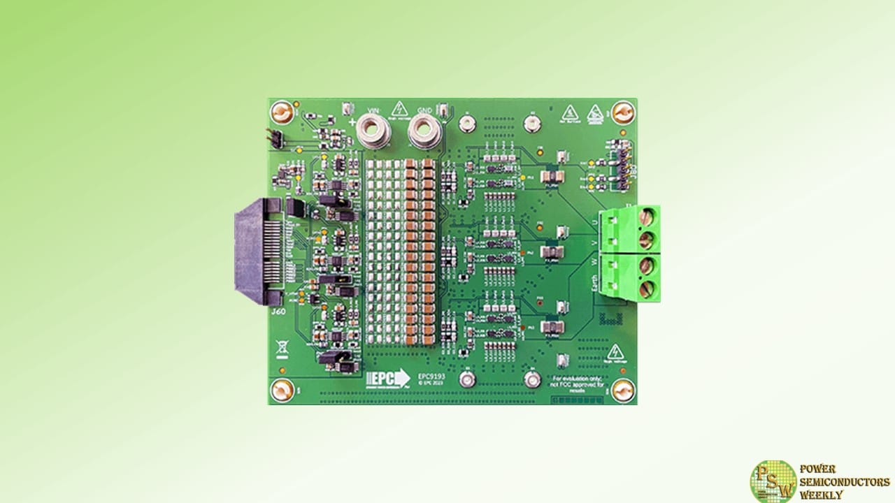
EPC announces the availability of the EPC9193, a 3-phase BLDC motor drive inverter using the EPC2619 eGaN® FET. The EPC9193 operates with a wide input DC voltage ranging from 14 V and 65 V and has two configurations – a standard unit and a high current version:
- The EPC9193 standard reference design uses a single FET for each switch position and can deliver up to 30 ARMS maximum output current.
- A high current configuration version of the reference design, the EPC9193HC, uses two paralleled FETs per switch position with the ability to deliver up to 60 Apk (42 ARMS) maximum output current.
Both versions of the EPC9193 contain all the necessary critical function circuits to support a complete motor drive inverter including gate drivers, regulated auxiliary power rails for housekeeping supplies, voltage, and temperature sense, accurate current sense, and protection functions. The EPC9193 boards measure just 130 mm x 100 mm (including connector).
Major benefits of a GaN-based motor drive are exhibited with these reference design boards, including lower distortion for lower acoustic noise, lower current ripple for reduced magnetic loss, and lower torque ripple for improved precision. The extremely small size of this inverter allows integration into the motor housing resulting in the lowest EMI, highest density, and lowest weight.
EPC provides full demonstration kits, which include interface boards that connect the inverter board to the controller board development tool for fast prototyping that reduce design cycle times.
“GaN-based inverters enhance motor efficiency and lower costs, expensive silicon MOSFET inverters”, said Alex Lidow, CEO of EPC. “This results in smaller, lighter, quieter motors with increased torque, range, and precision.”
Original – Efficient Power Conversion
-
Teledyne e2v HiRel announced the availability of radiation tolerant RF and Power products for the evolving New Space market. Qualified based on the EEE-INST-002 space grade standard, these plastic packaged products are qualified for the harsh environment of space with –55°C to +125°C temperature operating ratings, and are radiation tolerant for use in LEO, MEO, and GEO missions.
The RF products include several low noise amplifiers (LNA) and are ideal for demanding high-reliability space applications where low noise figure, minimal power consumption, and small footprint are critical to mission success. They are ideally suited for satellite communication systems that are increasing the power of radio signals so utilizing components with minimal noise and distortion help minimizing the degradation of digital signals.
These LNAs are developed in the radiation tolerant pHEMT technology semiconductor process technology. The monolithic microwave integrated circuit (MMIC) products are available in dual-flat no lead (DFN) plastic over molded SMT packages and are biased over single positive VDD supply voltages, eliminating the need for negative power rail voltages.
- The TDLNA002093SEP delivers a low noise figure of less than 0.37 dB, IDDQ from 30 mA to 100mA, and exceptional performance from 1 GHz (L-band) to 6 GHz (S-band) frequencies.
- The TDLNA0430SEP delivers an industry leading low noise figure of less than 0.35 dB, IDDQ of 60mA and exceptional performance from 0.3 GHz (UHF) to 3 GHz (S-band) frequencies.
- The TDLNA2050SEP delivers an industry leading low noise figure of less than 0.4 dB, IDDQ of 60mA and exceptional performance from 2.0 GHz (S-band) to 5 GHz (C-band) frequencies.
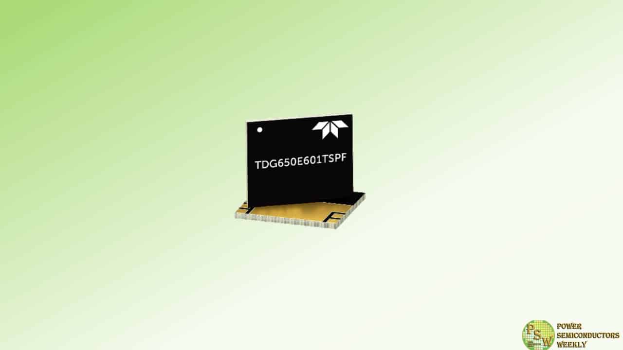
The Power products offerings include Gallium Nitride (GaN) technology High Electron Mobility Transistors up to 650V, currents up to 90 Amp, high switching frequencies, and low RDSON. These GaN solutions have easy gate-drive requirements and enable high power density designs with four times less space requirements than traditional MOSFETs. The TDG650E60xSP parts are available in extremely small non hermetic packages with either top-side and bottom-side thermal pads and are ideally suited for satellite power supply systems with space production screening.
“Today we’re announcing our New Space products offering of RF and Power products optimized for space applications,” said Mont Taylor, Vice President and Business Development Manager at Teledyne e2v HiRel. “These LNAs with their ultra low noise figures coupled with the high power density capabilities of GaN transistors, we believe these products will enable system designers with superior solutions for space based satellite communication applications.”Original – Teledyne e2v HiRel
-

Infineon Technologies AG filed a lawsuit, through its subsidiary Infineon Technologies Austria AG, against Innoscience (Zhuhai) Technology Company, Ltd., and Innoscience America, Inc. and affiliates. Infineon is seeking permanent injunction for infringement of a United States patent relating to gallium nitride (GaN) technology owned by Infineon.
The patent claims cover core aspects of GaN power semiconductors encompassing innovations that enable the reliability and performance of Infineon’s proprietary GaN devices. The lawsuit was filed in the district court of the Northern District of California.
Infineon alleges that Innoscience infringes the Infineon patent mentioned above by making, using, selling, offering to sell and/or importing into the United States various products, including GaN transistors for numerous applications, within automotive, data centers, solar, motor drives, consumer electronics, and related products used in automotive, industrial, and commercial applications.
“The production of gallium nitride power transistors requires completely new semiconductor designs and processes”, said Adam White, President of Infineon’s Power & Sensor Systems Division. “With nearly two decades of GaN experience, Infineon can guarantee the outstanding quality required for the highest performance in the respective end products. We vigorously protect our intellectual property and thus act in the interest of all customers and end users.”
Infineon has been investing in R&D, product development and the manufacturing expertise related to GaN technology for decades. Infineon continues to defend its intellectual property and protect its investments.
On 24 October 2023, Infineon announced the closing of the acquisition of GaN Systems Inc., becoming a leading GaN power house and further expanding its leading position in power semiconductors.
Infineon leads the industry with its GaN patent portfolio, comprising around 350 patent families. Market analysts expect the GaN revenue for power applications to grow by 49% CAGR to approx. US$2 billion by 2028 (source: Yole, Power SiC and GaN Compound Semiconductor Market Monitor Q4 2023). Gallium nitride is a wide bandgap semiconductor with superior switching performance that allows smaller size, higher efficiency and lower-cost power systems.
Original – Infineon Technologies
-
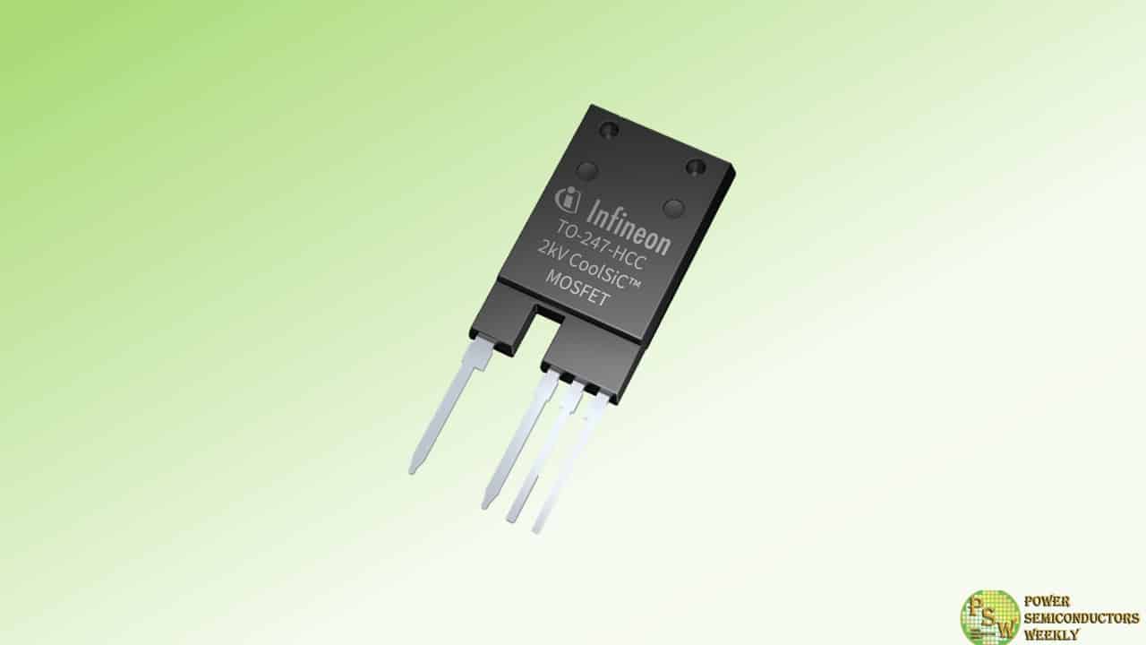
Infineon Technologies AG introduced the new CoolSiC™ MOSFETs 2000 V in the TO-247PLUS-4-HCC package to meet designers’ demand for increased power density without compromising the system’s reliability even under demanding high voltage and switching frequency conditions.
The CoolSiC MOSFETs offer a higher DC link voltage so that the power can be increased without increasing the current. It is the first discrete silicon carbide device with a breakdown voltage of 2000 V on the market and comes in a TO-247PLUS-4-HCC package with a creepage distance of 14 mm and clearance distance of 5.4 mm. With low switching losses, the devices are ideal for solar (e.g. string inverters) as well as energy storage systems and electric vehicle charging applications.
The CoolSiC MOSFET 2000 V product family is ideally suited for high DC link systems with up to 1500 V DC. Compared to 1700 V SiC MOSFETs, the devices also provide a sufficiently high overvoltage margin for 1500 V DC systems. The CoolSiC MOSFETs deliver a benchmark gate threshold voltage of 4.5 V and are equipped with a robust body diode for hard commutation. Due to the .XT connection technology, the components offer first-class thermal performance. They are also highly resistant to humidity.
In addition to the CoolSiC MOSFETs 2000 V, Infineon will soon be launching the matching CoolSiC diodes: The first launch will be the 2000 V diode portfolio in the TO-247PLUS 4-pin package in the third quarter of 2024, followed by the 2000 V CoolSiC diode portfolio in the TO-247-2 package in the final quarter of 2024. These diodes are particularly suitable for solar applications. A matching gate driver portfolio is also available.
The CoolSiC MOSFET 2000 V product family is available now. In addition, Infineon also offers a suitable evaluation board: the EVAL-COOLSIC-2KVHCC. Developers can use the board as a precise universal test platform to evaluate all CoolSiC MOSFETs and diodes 2000 V and the EiceDRIVER™ Compact Single Channel Isolated Gate Driver 1ED31xx product family through double pulse or continuous PWM operation.
Original – Infineon Technologies
-

EPC announced the publication of its Phase-16 Reliability Report, documenting continued work using test-to-fail methodology and adding specific guidelines for overvoltage specifications and improving thermo-mechanical reliability.
Compared to the Phase 15 Reliability Report, this version presents expanded data and analysis. It now includes a general overview of the wear-out mechanisms of primary concerns for a given application. New to this version of the report, is a description of how to forecast the reliability of a system in a realistic mission profile that combines periods of substantial and minor stress.
Adding to the existing knowledge base, this report includes significant new material on the thermo-mechanical wear-out mechanisms and overvoltage guidelines. Thermo-mechanical wear-out mechanisms include a study of the impact of die size and bump shape on temperature cycling (TC) reliability. This report also includes a study of overvoltage robustness for both the gate and the drain of GaN transistors.
This report is divided into the following sections:
- Section 1: Determining wear-out mechanisms using test-to-fail methodology.
- Section 2: Using test-to-fail results to predict device lifetime in a system.
- Section 3: Wear-out mechanisms
- Section 4: Mission-specific reliability predictions including solar, DC-DC, and lidar applications.
- Section 5: Summary and conclusions
- Appendix: Solder stencil design rules for reliable assembly of PQFN packaged devices
According to Dr. Alex Lidow, CEO and co-founder of EPC, “The release of our Phase-16 report satisfies a critical need for ongoing research into GaN device reliability. This report provides valuable insights on mission robustness, ensuring devices meet the demands of diverse applications.”
Original – Efficient Power Conversion
-
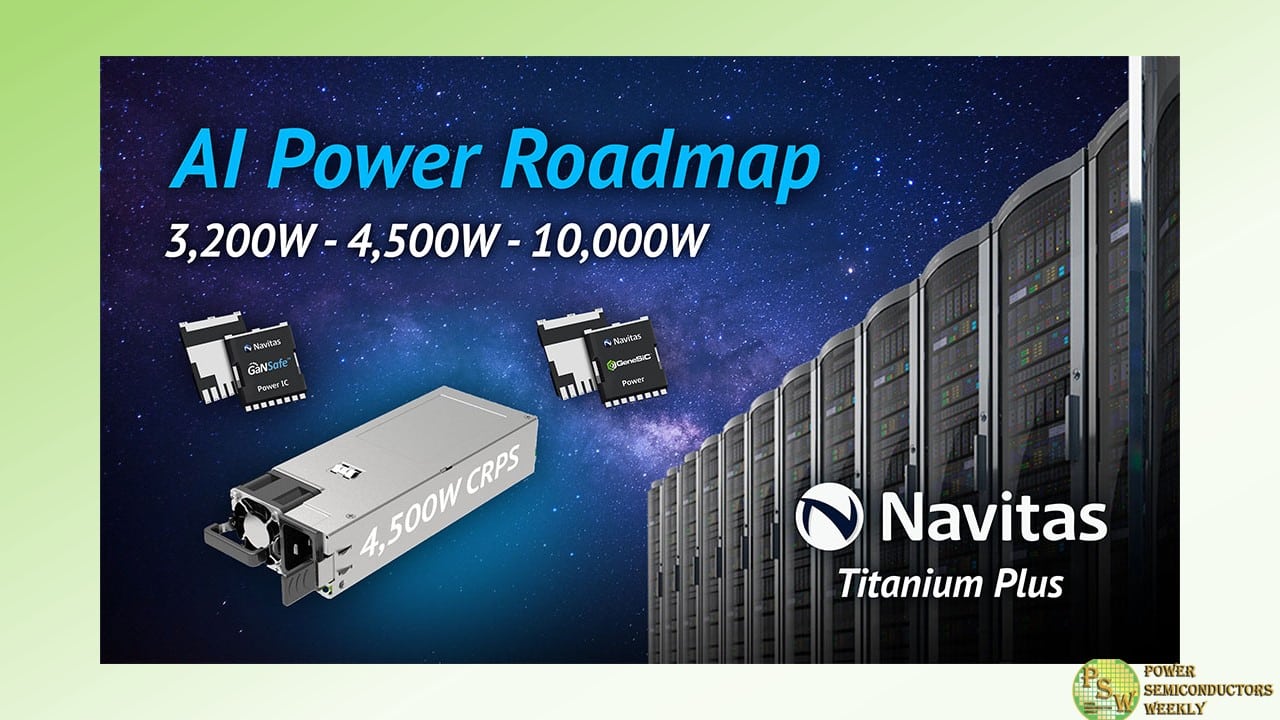
Navitas Semiconductor announced their AI data center technology roadmap for up to 3x power increase to support similar exponential growth in AI power demands expected in just the next 12-18 months.
Traditional CPUs require typically only 300W and the data center ac/dc power supplies would typically power the equivalent of 10 of these or 3,000W (3kW). High-performance AI processors like NVIDIA’s ‘Grace Hopper’ H100 are already demanding 700W each today, with next-gen ‘Blackwell’ B100 & B200 chips anticipated to increase to 1,000W or more by next year.
To meet this exponential power increase, Navitas is developing server power platforms which rapidly increase from 3kW to up to 10kW. In August 2023, Navitas introduced a 3.2kW data center power platform utilizing latest GaN technology enabling over 100W/in3 and over 96.5% efficiency. Now, Navitas is releasing a 4.5kW platform enabled by a combination of GaN and SiC to push densities over 130W/in3 and efficiencies over 97%. These two platforms have already generated significant market interest with over 20 data center customer projects in development expected to drive millions in GaN or SiC revenues starting this year.
Today, Navitas also announces its plans to introduce an 8-10kW power platform by the end of 2024 to support 2025 AI power requirements. The platform will utilize newer GaN and SiC technologies and further advances in architecture to set all-new industry standards in power density, efficiency and time-to-market. Navitas is already engaged with major data-center customers, with full platform launch anticipated in Q4 ’24, completing this 3x increase in power demands in only 12-18 months.
Navitas’ unique data-center design center is creating these system designs to address the dramatic increases in AI data center power requirements, and assist customers to deploy platforms quickly and effectively to meet the accelerated time-to-market demands of rapid AI advances. System designs include complete design collateral with fully-tested hardware, schematics, bill-of-materials, layout, simulation and hardware test results to maximize first-time-right designs and fast revenue generation.
“The rapid development and deployment of artificial intelligence (AI) into global data centers has created a dramatic and unexpected power challenge for our entire industry,” noted Gene Sheridan, Navitas’ CEO and Co-Founder. “Our investment in leading-edge GaN and SiC technologies, combined with our unique data-center design center capabilities, have positioned us well. Our team has really stepped up to the challenge, with a 3x power increase in less than 18 months.”
Original – Navitas Semiconductor
-
 LATEST NEWS / PROJECTS / SiC / WBG
Tianjin Economic-Technological Development Area Inked Investment Agreement with Vitesco Technologies
1 Min ReadTianjin Economic-Technological Development Area (TEDA) inked an investment agreement with Vitesco Technologies for a new project for NEV intelligent manufacturing and automotive electronic products. With the new project, Vitesco aims to strengthen its presence in TEDA by introducing new products such as silicon carbide power modules, 800V motor stators and rotors, EMR3 three-in-one axle drive systems, high-voltage inverters, battery control units, and gearbox controllers.
Vitesco Technologies is a global leader in automotive technology development and manufacturing, dedicated to providing advanced driving technology for sustainable mobility. Vitesco Technologies has been cooperating with TEDA for many years.
The establishment of its R&D center in TEDA in 2019 marks a major step forward in the NEV market, upgrading the Vitesco Tianjin Base into a super factory integrating R&D, testing, and production. Thomas Stierle, member of the Executive Board and head of Electrification Solutions Division of Vitesco Technologies, expressed confidence in China, Tianjin, and TBNA. He stated that Vitesco Technologies will continue to increase its investment in TBNA and deepen cooperation in manufacturing R&D and technological innovation.
-

Toshiba Electronic Devices & Storage Corporation has started mass production of a 3rd generation silicon carbide (SiC) 1700 V and drain current (DC) rating 250 A of SiC MOSFET module “MG250V2YMS3” for industrial equipment and has expanded its lineup.
The new product MG250V2YMS3 offers low conduction loss with low drain-source on-voltage (sense) of 0.8 V (typ.). It also offers low switching loss with low turn-on switching loss of 18 mJ (typ.) and low turn-off switching loss of 11 mJ (typ.). This helps to reduce power loss of equipment and the size of cooling device.
MG250V2YMS3 has a low stray inductance of 12 nH (typ.) and is capable of high-speed switching. In addition, it suppresses surge voltage in switching operation. Thus, it is available for high frequency isolated DC-DC converter.
Toshiba’s SiC MOSFET module of 2-153A1A package has a lineup of four existing products, MG250YD2YMS3 (2200 V / 250 A), MG400V2YMS3 (1700 V / 400 A), and MG600Q2YMS3 (1200 V / 600 A), including new products. This provides a wider range of product selection.
Toshiba will continue to meet the needs for high efficiency and the downsizing of industrial equipment.
Applications
Industrial equipment
- Inverters and converters for railway vehicles
- Auxiliary power supply for railway vehicles
- Renewable energy power generation systems
- Motor control equipment for industrial equipment
- High frequency DC-DC converters, etc.
Features
- Low drain-source on-voltage (sense):
VDS(on)sense=0.8 V (typ.) (ID=250 A, VGS=+20 V, Tch=25 °C) - Low turn-on switching loss:
Eon=18 mJ (typ.) (VDD=900 V, ID=250 A, Tch=150 °C) - Low turn-off switching loss:
Eoff=11 mJ (typ.) (VDD=900 V, ID=250 A, Tch=150 °C) - Low stray inductance:
LsPN=12 nH (typ.)
Original – Toshiba
