-

Texas Instruments introduced two new power conversion device portfolios to help engineers achieve more power in smaller spaces, providing the highest power density at a lower cost. TI’s new 100V integrated gallium nitride (GaN) power stages feature thermally enhanced dual-side cooled package technology to simplify thermal designs and achieve the highest power density in mid-voltage applications at more than 1.5kW/in3.
TI’s new 1.5W isolated DC/DC modules with integrated transformers are the industry’s smallest and most power-dense, helping engineers shrink the isolated bias power-supply size in automotive and industrial systems by over 89%. Devices from both portfolios will be on display at this year’s Applied Power Electronics Conference (APEC), Feb. 25-29 in Long Beach, California.
“For power-supply designers, delivering more power in limited spaces will always be a critical design challenge,” said Kannan Soundarapandian, general manager of High Voltage Power at TI. “Take data centers, for example – if engineers can design power-dense server power-supply solutions, data centers can operate more efficiently to meet growing processing needs while also minimizing their environmental footprint. We’re excited to continue to push the limits of power management by offering innovations that help engineers deliver the highest power density, efficiency and thermal performance.”
Increase power density and efficiency with 100V integrated GaN power stages
With TI’s new 100V GaN power stages, LMG2100R044 and LMG3100R017, designers can reduce power-supply solution size for mid-voltage applications by more than 40% and achieve industry-leading power density of over 1.5kW/in3, enabled by GaN technology’s higher switching frequencies. The new portfolio also reduces switching power losses by 50% compared to silicon-based solutions, while achieving 98% or higher system efficiency given the lower output capacitance and lower gate-drive losses. In a solar inverter system, for example, higher density and efficiency enables the same panel to store and produce more power while decreasing the size of the overall microinverter system.A key enabler of the thermal performance in the 100V GaN portfolio is TI’s thermally enhanced dual-side cooled package. This technology enables more efficient heat removal from both sides of the device and offers improved thermal resistance compared to competing integrated GaN devices.
To learn more about the benefits of TI’s 100V GaN power stages for mid-voltage applications, read the technical article, “4 mid-voltage applications where GaN will transform electronic designs.”
Shrink bias power supplies by more than 89%
With over eight times higher power density than discrete solutions and three times higher power density than competing modules, TI’s new 1.5W isolated DC/DC modules deliver the highest output power and isolation capability (3kV) for automotive and industrial systems in a 4mm-by-5mm very thin small outline no-lead (VSON) package. With TI’s UCC33420-Q1 and UCC33420, designers can also easily meet stringent electromagnetic interference (EMI) requirements, such as Comité International Spécial des Perturbations Radioélectriques (CISPR) 32 and 25, with fewer components and a simple filter design.The new modules use TI’s next-generation integrated transformer technology, which eliminates the need for an external transformer in a bias supply design. The technology allows engineers to shrink solution size by more than 89% and reduce height by up to 75%, while cutting bill of materials by half compared to discrete solutions.
With the first automotive-qualified solution in this small package, designers can now reduce the footprint, weight and height of their bias supply solution for electric vehicle systems such as battery management systems. For space-constrained industrial power delivery in data centers, the new module enables designers to minimize printed circuit board area.
To learn more about the benefits of TI’s 1.5W isolated DC/DC modules, read the technical article, “How a new isolated DC/DC module can help solve power-density challenges.”
Pushing the limits of power at APEC 2024
These new devices are the latest ways TI is pushing power further and making innovation possible for engineers everywhere. At APEC 2024, TI will showcase the latest automotive and industrial designs for 48V automotive power; the first USB Power Delivery Extended Power Range full charging solution on the market; an 800V, 300kW silicon carbide-based traction inverter; high-efficiency power for server motherboards; and more.- Saturday, Feb. 24-Thursday, Feb. 29: Visit TI in the Long Beach Convention & Entertainment Center, Booth No. 1145. See TI.com/APEC for more information.
- Wednesday, Feb. 28 at 12 p.m. Pacific time: TI General Manager of Industrial Power Design Services Robert Taylor will present an industry session, “To Power Density and Beyond: Breaking Through Barriers to Achieve the Highest Power Density.” He will discuss innovations in packaging, integration and system-level techniques that are making greater power density possible.
- Throughout APEC: TI power experts will lead 20 industry and technical sessions to address power-management design challenges. The full schedule of TI experts’ industry and technical sessions is available at TI.com/APEC.
Original – Texas Instruments
-
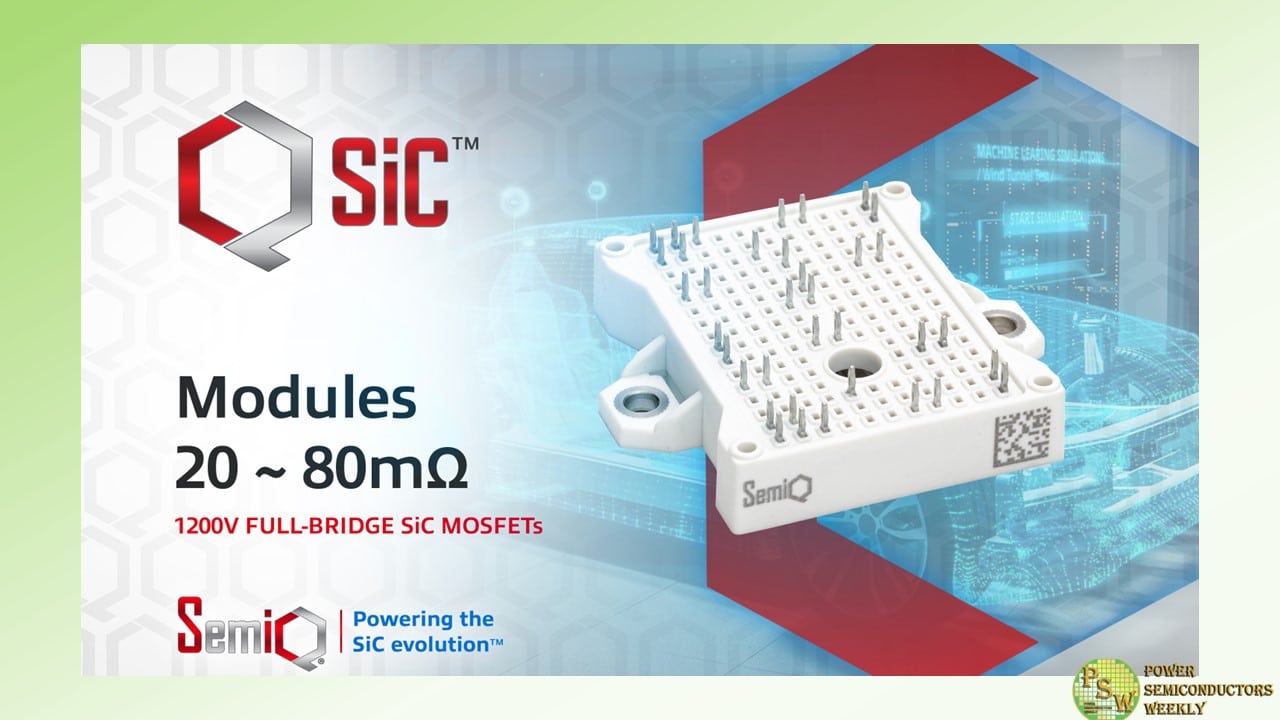
SemiQ Inc. unveiled the latest addition to the company’s QSiC™ family. The QSiC 1200V SiC MOSFET modules in full-bridge configurations deliver near zero switching loss, significantly improving efficiency, reducing heat dissipation, and allowing the use of smaller heatsinks.
With a high breakdown voltage exceeding 1400V, the QSiC modules in full-bridge configurations withstand high-temperature operation at Tj = 175°C with minimal Rds(On) shift across the entire temperature spectrum. Crafted from high-performance ceramics, SemiQ’s modules achieve exceptional performance levels, increased power density, and more compact designs—especially in high-frequency and high-power environments.
Consequently, they are well-suited for demanding applications that require bidirectional power flow or a broader range of control, such as solar inverters, drives and chargers for Electric Vehicles (EVs) DC-DC converters and power supplies.
In solar inverter applications, SemiQ’s technology empowers designers to achieve greater efficiency – reaching as high as 98% – as well as more compact designs. It helps reduce heat loss, improve thermal stability, and enhance reliability, backed by over 54 million hours of HTRB/H3TRB testing. The 1200V MOSFETs also maximize efficiency gains in DC-DC converters while enhancing reliability and minimizing power dissipation.
To guarantee a stable gate threshold voltage and premium gate oxide quality for each module, SemiQ conducts gate burn-in testing at the wafer level. In addition to the burn-in test, which contributes to mitigating extrinsic failure rates, various stress tests—including gate stress, high-temperature reverse bias (HTRB) drain stress, and high humidity, high voltage, high temperature (H3TRB)—are employed to attain the necessary automotive and industrial grade quality standards. The devices also offer extended short-circuit ratings, and all parts have undergone testing surpassing 1400V.
“At SemiQ, our commitment lies in the meticulous optimization and customization of each module, ensuring they not only meet but exceed the unique demands of high-efficiency, high-power applications,” said Dr. Timothy Han, President at SemiQ. “We believe in empowering innovation through tailored solutions, and our SiC modules exemplify the pinnacle of performance, precision, and reliability in every customized design.”
SemiQ is set to debut its QSiC product family in SOT-227, half-bridge, and full-bridge packages at the Applied Power Electronics Conference (APEC) in Long Beach, CA, from February 25 to 29, 2024. Attendees at SemiQ’s booth #2245 will be the first to explore the newest additions to the QSiC lineup. Schedule a meeting with the SemiQ team using online calendar or email at media@semiq.com.
SemiQ’s new 1200V modules in full-bridge packages are available in 20mΩ, 40mΩ, 80mΩ SiC MOSFETs categories:
Part Numbers Circuit Configuration Ratings, Packages RdsOn mΩ GCMX020A120B2H1P Full-bridge 1200V/102A, B2 20 GCMX040A120B2H1P Full-bridge 1200V/56A, B2 40 GCMX080A120B2H1P Full-bridge 1200V/27A, B2 80 GCMX020A120B3H1P Full-bridge 1200V/93A, B3 20 GCMX040A120B3H1P Full-bridge 1200V/53A, B3 40 Original – SemiQ
-

Cambridge GaN Devices (CGD), the fabless, clean-tech semiconductor company that develops energy-efficient GaN-based power devices that make greener electronics possible, will be present at the upcoming APEC 2024, IEEE Applied Power Electronics Conference and Exposition. In addition to having its largest ever booth at the show, the company will contribute with a number of papers including an analysis of how GaN can play a part in supporting the exponential growth in power demanded by datacentres as the use of Artificial Intelligence (AI) proliferates.
GIORGIA LONGOBARDI | CHIEF EXECUTIVE OFFICER, CGD:
“With datacentres now demanding 100kW per rack and predicting even more in the very near future, power system designers are looking to employ GaN devices in new architectures. At CGD we are addressing this challenge with new devices and reference designs which we will be discussing at APEC, along with many other applications where GaN can play a huge role in enabling sustainable electronics solutions that are more efficient, have high performance and are more compact.”
CGD will present three papers at APEC:
- Tuesday 27th February, 15.00-15.30 – ‘How ICeGaN™ technology can address the datacentre challenges that digitalisation brings’, with Andrea Bricconi, Chief Commercial Officer, CGD and Peter Di Maso, VP of Business Development (Americas) CGD.
- Wednesday 28th February, 09.10-09.30 – ‘Evaluation of GaN HEMT dv/dt Immunity and dv/dt induced false turn-on energy loss’, with Nirmana Perera, Application Engineer, CGD.
- Thursday 29th February, 09:45 – 10:10: ‘Monolithic integration addresses the design challenges of GaN Power devices’, with Di Chen, Director of Business Development & Technical Marketing, CGD.
On booth 1553, CGD will present a range of demos designed to showcase industry’s first easy-to-use and scalable 650 V GaN HEMT family. ICeGaN™ H2 single-chip eMode HEMTs can be driven like a MOSFET, without the need for special gate drivers, complex and lossy driving circuits, negative voltage supply requirements or additional clamping components.
Addressing the increase in power required by server and industrial applications, CGD will show a 350 W PFC/LLC reference design using ICeGaN (650 V, 55 mΩ, H2 series). With a board power density of 23 W/in3, the bridgeless CrM Totem Pole PFC plus half-bridge LLC design has a peak efficiency of 95%, (93% average) and a no-load power consumption of 150 mW.
ANDREA BRICCONI | CHIEF COMMERCIAL OFFICER, CGD:
“GaN is now accepted as a reliable and proven technology that is able to deliver high efficiency and power density simultaneously. Datacentres, with their insatiable need for power, are an obvious application for GaN, but there are many other consumer, industrial and automotive applications where GaN can also demonstrate the ability to be a disruptive technology. CGD has delivered industry’s most easy-to-use GaN technology – ICeGaN – and we are keen to share our ideas with the audience at APEC.”
Original – Cambridge GaN Devices
-

Micro Commercial Components unveiled 1700V SiC MOSFET – SICW400N170A-BP. Designed to elevate power conversion in a range of applications, this MOSFET features ultra-low on-resistance of only 400mΩ and high blocking voltage capability. SICW400N170A-BP SiC MOSFET enables high-speed switching while ensuring minimal conduction losses — essential requirements for optimizing frequency-dependent systems.
A standard, yet durable TO-247AB package delivers effective operation at a gate-source voltage of 20V with superior thermal stability and an operating junction temperature of +175°C.
This unwavering reliability in harsh conditions only adds to the component’s appeal and versatility for various high-voltage applications, including EV charging stations and renewable energy systems.
Features & Benefits:
- High blocking voltage capability (1700V)
- Ultra-low on-resistance (400mΩ) enhances efficiency
- Low capacitance enables faster switching
- Excellent thermal stability
- High operating junction temperature (to +175°C)
- Standard TO-247AB package
Original – Micro Commercial Components
-
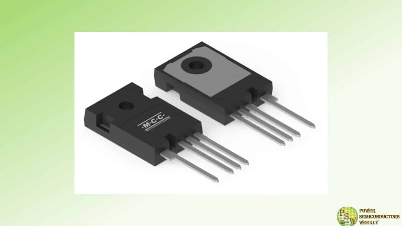
Micro Commercial Components introduced its latest high-performance component — 1200V SiC N-channel MOSFET. With an impressively low on-resistance of just 28mΩ at a gate-source voltage of 18V, SICW028N120A4-BP is engineered to deliver in demanding high-power applications.
Housed in a TO-247-4 package, this MOSFET works well with the popular D2PAK 4-pin footprint and includes a Kelvin source pin for significant reduction in switching losses and a boost in energy efficiency.
A high operating junction temperature of up to +175°C and excellent thermal stability ensure this new SiC MOSFET will revolutionize power management in a diverse range of industrial and commercial devices that must perform in harsh conditions.
Features & Benefits:
- 1200V blocking voltage capability
- 28mΩ low on-resistance
- Kelvin source pin for enhanced switching
- Avalanche ruggedness for durability
- Excellent thermal stability
- High operating junction temperature range (+175°C)
- D2PAK-compatible 4-pin TO-247-4 package
Original – Micro Commercial Components
-

Innoscience Technology has launched a new 100V bi-directional member of the company’s VGaN IC family. The first family of VGaN devices rated 40V with wide on-resistance range (1.2mOhm – 12mOhm) have been successfully deployed in the USB OVP of mobile phones such as OPPO, OnePlus etc.
The new 100V VGaN (INV100FQ030A) can be employed to achieve high efficiency in 48V or 60V battery management systems (BMS), as well as for high-side load switch applications in bidirectional converters, switching circuits in power systems, and other fields. Such device it is ideal in application such as home batteries, portable charging station, e-scooters, e-bikes etc.
One VGaN replaces two back-to-back Si MOSFETs; they are connected with a common drain to achieve bidirectional switching of battery charging and discharging, further reducing on-resistance and loss significantly with respect to traditional Silicon solution. BOM count, PCB space and costs are also reduced accordingly.
The INV100FQ030A 100V VGaN IC supports two-way pass-through, two-way cut-off and no-reverse-recovery modes of operation. Devices feature an extremely low gate charge of just 90nC, ultra-low dynamic on-resistance of 3.2mΩ and small, 4x6mm package size.
Dr. Denis Marcon, General Manager, Innoscience Europe comments: “Innoscience’s continuous innovation and development of our core technology plus our 8-inch wafer GaN IDM model will accelerate the miniaturization of systems, making them more efficient and energy-saving.”
Innoscience ‘s 100V GaN series products are in mass production in En-FCQFN (exposed top side cooling) and FCQFN packaging.
Original – Innoscience Technology
-
Qorvo® will showcase its latest power management innovations at the upcoming Applied Power Electronics Conference (APEC) from Feb. 26-28, at the Long Beach Convention Center in California. Attendees are invited to visit the Qorvo booth #1857 to explore the latest advancements in SPICE simulation, silicon carbide (SiC) and battery management technologies.
Qorvo will feature the following highlights at APEC 2024:
QSPICE™ Simulation Software Showcase
APEC attendees can experience the next level of simulation with Qorvo’s advanced QSPICE tool during three insightful training sessions and engage in a Q&A with the tool’s creator, Mike Engelhardt. For those unable to attend APEC, the sessions will be available on the Qorvo YouTube channel in March.Training Session Schedule:
- Tuesday, Feb. 27, 10-10:20 a.m.: The QSPICE User-Interface
- Tuesday, Feb. 27, 3-3:20 p.m.: Importing 3rd Party Models
- Wednesday, Feb. 28, 10-10:20 a.m.: Anatomy of a Macro Model Done Right
Launch of Inaugural SiC Module Family
Qorvo will unveil its first SiC module family, featuring an innovative cascode JFET architecture. This highly integrated device family simplifies high-voltage designs and offers exceptional thermal and electrical performance due to low switching losses, low thermal resistance and RDS(on) as low as 9.4mΩ.Battery Management Demonstrations
Visitors to the booth can see Qorvo’s wireless battery management debut with a demonstration showcasing a remote battery pack monitoring and state of charge solution, created in combination with Qorvo’s IoT microcontroller.Original – Qorvo
-

Infineon Technologies AG announced a collaboration with Worksport. Worksport Ltd. will use Infineon’s GaN power semiconductors GS-065-060-5-B-A in the converters for its portable power stations to increase efficiency and power density. Enabled by Infineon’s GaN transistors, the power converters will be lighter and smaller in size with reduced system costs. In addition, Infineon will support Worksport in the optimization of circuits and layout design to further reduce size and increase power density.
“Infineon’s high-quality standard and solid supply chain provide us with the best components to ensure power-dense converters for our COR system product line and contribute to a first-class end product performance,” said Worksport CEO Steven Rossi.
The company’s COR battery system can be integrated into a pickup truck or recharged by any solar panel or wall outlet. By replacing the former silicon switch in the power converter with Infineon’s GaN power semiconductors and operating the transistors at higher switching frequency, Worksport will be able to reduce the battery system weight by 33 percent and system costs by up to 25 percent.
The working relationship with Infineon will also help Worksport to reduce CO2 in the manufacturing process. GaN is proving itself as a game-changing technology across many markets and applications. For example, in data centers, GaN solutions have a global energy savings potential of 21 TWh annually, 10 million tons of Carbon Dioxide (CO2) equivalent.
“In order to further drive electrification and decarbonization, the industry’s power designs require innovation,” said Johannes Schoiswohl, Business Line Head GaN Systems of Infineon’s Power & Sensor Systems Division. “With our GaN power semiconductors we enable Worksport to create the next generation portable power stations that users require.”
Infineon’s GS-065-060-5-B-A is an Automotive-grade 650 V enhancement mode GaN-on-Silicon power transistor. It offers very low junction-to-case thermal resistance for demanding high power applications such as on-board chargers, industrial motor drives and solar inverters. Furthermore, it features simple gate drive requirements (0 V to 6 V) and a transient tolerant gate drive (-20 / +10 V).
Original – Infineon Technologies
-

Leapers Semiconductor introduced a new 62 mm package SiC module product portfolio, achieving top-tier performance in the industry. The modules adopt the widely used 62 mm module half-bridge topology design in the industrial field, using high-quality mature chips. It boasts high voltage resistance, outstanding power density, high short-circuit tolerance, and a temperature coefficient 1.4 times better than industry standards.
The 62 mm SiC modules include voltage resistance specifications of 1200V and 1700V, meeting the demands of high-power applications, especially suitable for applications in the smart grid, rail transit, energy storage, and power supplies.
Because of the use of leading-edge chip solutions in the industry and the application of low thermal resistance and low stray capacitance packaging technology, along with the use of Si3N4 AMB low thermal resistance substrate, Leapers’ 62 mm SiC product excels in power density, short-circuit current withstand capability, thermal resistance, and other capabilities. Particularly under high junction temperature conditions, the module’s conduction and switching losses significantly outperform industry standards.
Technical Features:- Voltage resistance options: 1200V or 1700V
- Outstanding current output capability
- Temperature coefficient index better than industry standards
- Low losses, excellent short-circuit current withstand capability
- Si3N4 AMB, low thermal resistance
Currently, Leapers 62 mm SiC modules have undergone bench tests and received orders, involving applications such as grid inverters and auxiliary inverters for rail transit vehicles. Downstream customers include domestic power grid and overseas rail transit enterprises.Original – Leapers Semiconductor
-

VMAX, a leading Chinese manufacturer of power electronics and motor drives for new energy vehicles, has selected the new CoolSiC™ hybrid discrete with TRENCHSTOP™ 5 Fast-Switching IGBT and CoolSiC Schottky Diode from Infineon Technologies AG for its next generation 6.6 kW OBC/DCDC on-board chargers.
Infineon’s components come in a D²PAK package and combine ultra-fast TRENCHSTOP 5 IGBTs with half-rated free-wheeling SiC Schottky barrier diodes to achieve a perfect cost-performance ratio for both hard and soft switching topologies. With their superior performance, optimized power density and leading quality, the power devices are ideally suited for VMAX’s on-board chargers.
“We are proud to choose Infineon’s CoolSiC Hybrid device in our next-generation OBC, achieving higher reliability, stability, improved performance, and power density. This deepens our already strong partnership with Infineon and drives technological application innovation through close collaboration, working together to promote the thriving development of new energy vehicles,” said Jinzhu Xu, PL Director& Chief Engineer, R&D Department at VMAX.
“We are excited to strengthen our partnership with VMAX with our highly efficient hybrid products,” said Robert Hermann, Vice President for Automotive High Voltage Chips and Discretes at Infineon. “Together, we will continue to drive e-mobility advancements, providing efficient solutions that meet the requirements of the industry in terms of performance, quality and system cost.”
With its fast, hard switching TRENCHSTOP 5 650 V IGBT co-packed with zero reverse recovery CoolSiC Schottky diode, the hybrid discrete benefits from very low switching losses at switching speeds above 50 kHz. This makes the device an excellent option for high-power electric vehicle charging systems.
In addition, the robust 5 th generation CoolSiC Schottky diode offers increased robustness against surge currents, maximizing reliability. Furthermore, the diffusion soldering of the SiC diode has improved the thermal resistance (R th) to the package for small chip sizes, resulting in increased power switching capability.
With these features, it enables optimum system reliability and longevity, meeting the stringent requirements of the automotive industry. To further maximize compatibility with existing designs, the product also features a pin-to-pin compatible design based on the widely used D²PAK package.
Original – Infineon Technologies
