-

Wolfspeed, Inc. announced the expansion of an existing long-term silicon carbide wafer supply agreement with a leading global semiconductor company. The expanded agreement, which is now worth approximately $275 million in total, calls for Wolfspeed to supply the company with 150mm silicon carbide bare and epitaxial wafers, reinforcing both companies’ visions for an industry-wide transition from silicon to silicon carbide semiconductor power devices.
“As the global leader in silicon carbide wafer production, Wolfspeed is uniquely positioned to be a critical supplier of high-quality and advanced silicon carbide materials at scale. We will continue to be an important partner to power device manufacturers who need the highest-quality silicon carbide wafers to service their customers,” said Dr. Cengiz Balkas, SVP and GM of Materials for Wolfspeed.
“This agreement further strengthens our long-time partnership with a best-in-class power semiconductor manufacturer. Our collective efforts are helping to address the rapidly expanding opportunity for silicon carbide and better address the unfulfilled demand that exists in the marketplace today.”
The adoption of silicon carbide-based power solutions is rapidly growing across multiple markets, including industrial and EVs. Silicon carbide solutions enable smaller, lighter and more cost-effective designs, converting energy more efficiently to unlock new applications in electrification. This supply agreement will enable silicon carbide applications in a broad range of industries, such as: renewable energy and storage, electric vehicles, charging infrastructure, industrial power supplies, traction and variable speed drives.
Wolfspeed is the global leader in the manufacturing of silicon carbide wafers and epitaxial wafers. The company is currently expanding its manufacturing capacity in the United States and has plans to open a new, automated materials factory in Siler City, North Carolina later this year that will produce 200mm silicon carbide wafers. The new materials factory will increase Wolfspeed’s current materials production capacity by ten times.
Original – Wolfspeed
-

JEDEC Solid State Technology Association announced the publication of JEP198: Guideline for Reverse Bias Reliability Evaluation Procedures for Gallium Nitride Power Conversion Devices. Developed by JEDEC’s JC-70.1 Gallium Nitride Subcommittee, JEP198 is available for free download from the JEDEC website.
JEP198 presents guidelines for evaluating the Time Dependent Breakdown (TDB) reliability of GaN power transistors. It is applicable to planar enhancement-mode, depletion-mode, GaN integrated power solutions, and cascode GaN power transistors.
This publication covers suggested stress conditions and related test parameters for evaluating the TDB reliability of GaN power transistors using the off-state bias. The stress conditions and test parameters for both High Temperature Reverse Bias Stress and Application Specific Stress-Testing are designed to evaluate the reliability of GaN transistors over their useful lifetime under accelerated stress conditions.
“We are becoming more dependent on power electronics in all facets of our daily lives. As such, the technologies behind those systems are advancing and so too must the device-specific qualification processes. The new GaN-focused Guideline for Reverse Bias Reliability Evaluation is a critical step toward achieving that goal,” said Ron Barr, VP of Quality and Reliability, Transphorm and Co-Chair of the Task Group 701_1.
“This was a collaborative effort conducted by both GaN semiconductor and end product manufacturers. I’m proud of the work the task group delivered. It is an important framework to ensure cross-industry uniformity that will, in the end, provide power system manufacturers the necessary confidence when designing with GaN devices.”
“With the rise of renewable energy and electrification of our lives, the efficiency of power semiconductors is becoming more critical. This is where GaN power semiconductors have proven to be a valuable technology. The Guideline for Reverse Bias Reliability Evaluation is another step in improving confidence in GaN Technology and the products that are on and being brought to market,” said Dr. Kurt Smith, VP of Reliability and Qualification at VisIC Technologies and Chair of JC-70.1.
“This document was developed through collaboration of the multi-corporation team of industry experts to represent the best practices for evaluating GaN devices. It was a long multi-year process to reach consensus and the team is to be commended for the quality document and all of the hard work that went into it.”
Original – JEDEC
-
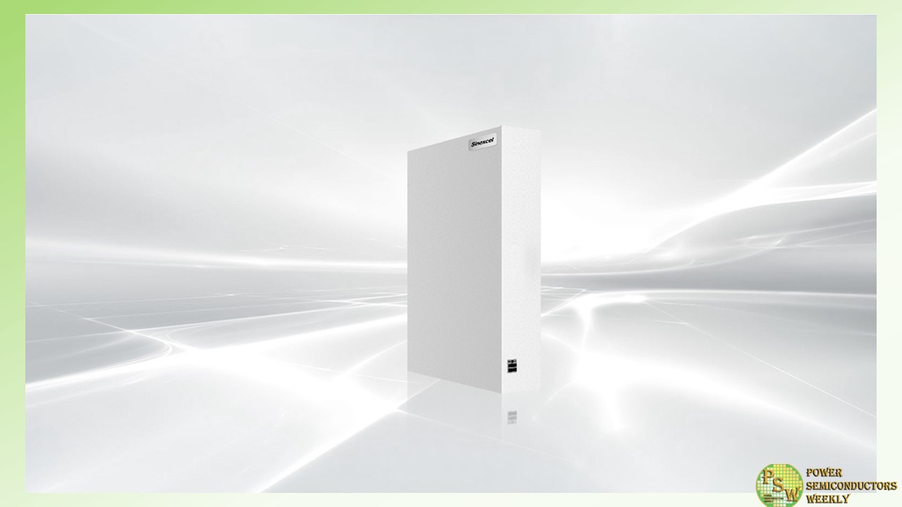
Infineon Technologies AG announced a partnership with Shenzhen based Sinexcel Electric Co., Ltd., a global leader in core power equipment and solutions for the Energy Internet. Infineon will provide Sinexcel with its industry-leading 1200 V CoolSiC™ MOSFET power semiconductor devices in combination with EiceDRIVER™ compact 1200 V single-channel isolated gate drive ICs to further improve the efficiency of energy storage systems.
Driven by the carbon peaking and carbon neutrality strategy and the new energy wave, the domestic energy storage market has maintained sustained and rapid development in recent years. According to the Chinese Ministry of Industry and Information Technology, in the first half of 2023, the newly installed capacity of energy storage reached 8.63 GWh, equivalent to the total installed capacity of previous years.
The efficiency and power density of energy storage systems are important factors of product competitiveness, while the size, weight and cost of energy storage systems are closely related to the energy conversion efficiency and directly affect the product cost. Therefore, power semiconductor components play a crucial role.
“The SiC power solution is an important component for future green energy production and storage applications. Infineon’s cooperation with Sinexcel in the field of energy storage inverters enables energy storage systems to achieve advantages such as high efficiency, small size, and light weight, providing a solid guarantee for high-reliability and high-performance energy storage systems,” said Mr. Yu Daihui, Senior Vice President of Infineon Technologies and Head of Green Industrial Power Division in Greater China.
“By using Infineon’s SiC devices, Sinexcel’s energy storage products are obviously more compact and flexible, with significantly higher efficiency and lower losses, which reduces the heat dissipation cost of systems, is conducive to the long-term efficient and stable operation of products, and helps end users improve their operational stability and shorten their return on investment cycle.
This greatly improves the system competitiveness of our products and enhances the trust of clients in our energy storage products and the brand awareness of Sinexcel. We hope that in the future, Infineon will further provide high-performance and high-stability components to help enhance the competitiveness of Sinexcel’s products on the client side,” said Mr.Wei Xiaoliang, Deputy General Manager of Sinexcel.
With more than 20 years of product development and application experience in the SiC field, Infineon has been working nonstop to develop more sophisticated SiC products. Due to their high power density, Infineon’s 1200 V CoolSiC MOSFETs can reduce losses by 50 percent and provide ~2 percent additional energy without increasing the battery size, which is especially beneficial for high-performance, lightweight and compact energy storage solutions.
By using Infineon’s 1200 V CoolSiC MOSFETs and EiceDRIVER compact 1200 V single-channel isolated gate drive ICs, Sinexcel’s energy storage converters achieve high power density, minimum electromagnetic radiation and interference, high protection performance and high reliability. This allows a system efficiency of up to 98 percent, which is 1 percent higher than that of traditional solutions, reaching the industry-leading level and better meeting the needs of on-grid and off-grid energy storage applications in both domestic and overseas markets.
Original – Infineon Technologies
-

Navitas Semiconductor and SHINRY, global industry leader of on-board power supply and strategic supplier to Honda, Hyundai, BYD, Geely, XPENG, BAIC and many more leading automobile manufacturers, announced the opening of an advanced, joint R&D power laboratory to accelerate the development of New-Energy Vehicle (NEV) power systems enabled by Navitas’ GaNFast™ technology.
Next-gen gallium nitride (GaN) is replacing legacy silicon power chips due to superior high-frequency and high-efficiency characteristics. GaN delivers faster charging, faster acceleration and longer-range, accelerating market adoption of NEVs and the transition from fossil fuels to clean, renewable energy.
On January 16th, 2024, Peter (Jingjun) Chen, COO of SHINRY, along with Navitas’ Gene Sheridan, CEO and Navitas’ Charles (Yingjie) Zha, VP and GM plus other senior executives attended the joint lab’s opening ceremony at SHINRY headquarters in Shenzhen.
The joint lab accelerates development projects, with leading-edge GaN technology combining with innovative system-design skills and engineering talent to enable unprecedented high power density, lightweight, efficient designs that translate to faster charging and extended range, with faster time-to-market.
The joint lab brings together experienced, highly-professional engineers from Navitas and SHINRY to build efficient, collaborative R&D platforms. Navitas’ own dedicated EV system Design Center, located in Shanghai will provide comprehensive technical support for the joint lab.
Navitas will not only supply SHINRY with leading-edge, trusted power devices, but will also engage in system-level R&D from the initial stages of product specification and design, through to test platforms and customized packaging solutions. The result will be more efficient, higher power density, more reliable, and cost-effective power systems for NEVs.
“SHINRY always pursues technological innovation. As early as 2012, SHINRY began applying Silicon Carbide (SiC) MOS, and in 2019, SHINRY initiated research on the application of GaN and has been actively seeking strategic partners.” said Peter (Jingjun) Chen, COO of SHINRY.
“As an advanced supplier in the field, Navitas will assist in creating more advanced, energy-efficient, and higher-efficiency power system products. I believe the establishment of this joint lab will comprehensively accelerate the design and market launch of SHINRY’s products and further enhance the market competitiveness of SHINRY products.”
“We are excited to join with SHINRY to establish a new lab for next-gen power semiconductors, assisting SHINRY in creating advanced power systems.” said Gene Sheridan, Navitas’ co-founder & CEO. “SHINRY’s mission to change the way of travel aligns closely with Navitas’ Electrify Our World™ mission. We believe that through our joint efforts, leading GaN technologies will enter the power systems of NEVs for more end-users, contributing to the vigorous growth of the new energy industry.
Original – Navitas Semiconductor
-
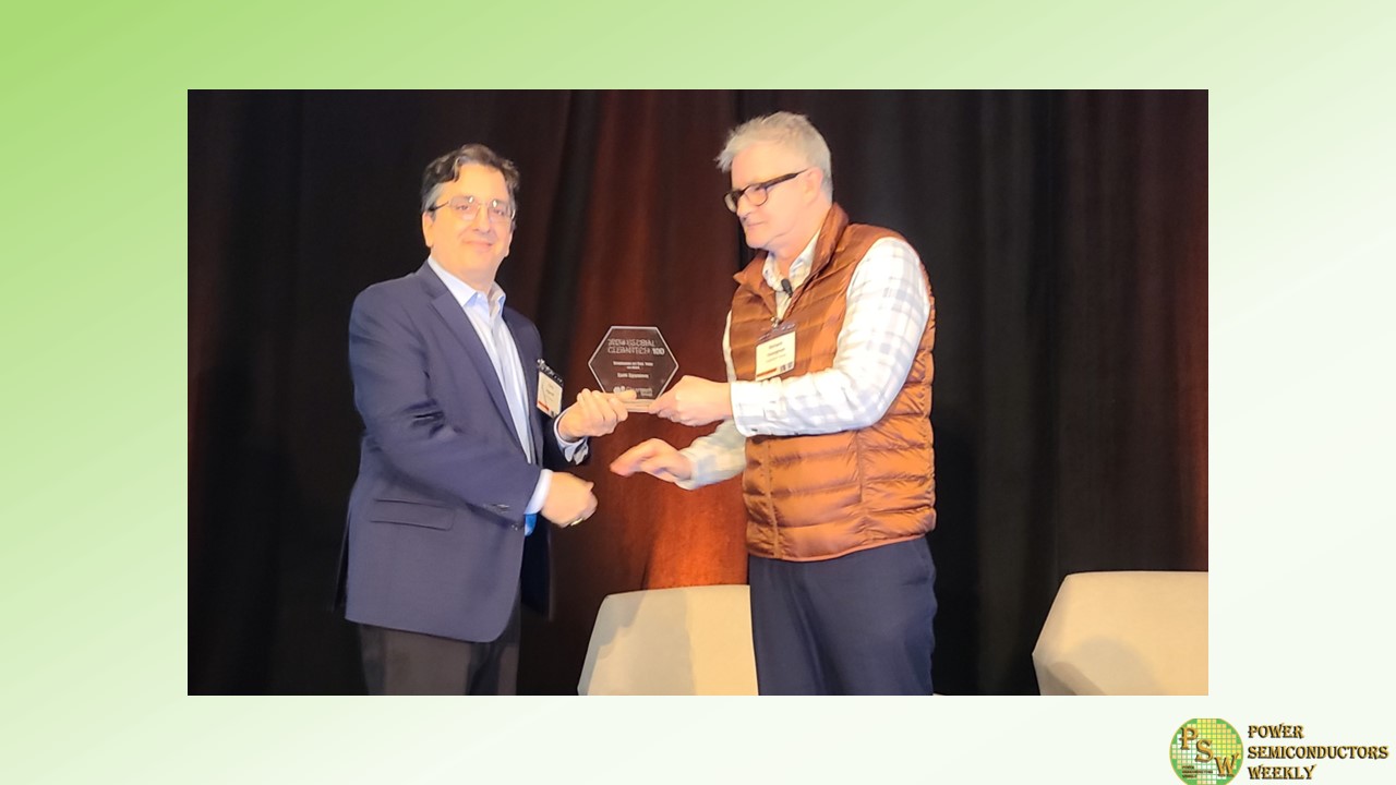
Acquired by Infineon Technologies in October 2023, GaN Systems has been recognized as the “Graduate Of The Year” by The Global Cleantech 100. The announcement was made at Cleantech Forum North America in San Francisco.
The award recognizes the exceptional contribution legacy GaN Systems has made to sustainable innovation and their successful management team as rated by the financial investors on the 80-member Cleantech Group Expert Panel. This 2024 award rounds out several years of recognition in GaN Systems’ sustainability journey which includes entry in to the Global Cleantech 100 Hall of Fame (1 of only 14 companies ever) and the 2023 Global Cleantech 100 winner (1 of only 100 companies globally in 2023).
The acquisition of GaN Systems has significantly accelerated Infineon’s gallium nitride (GaN) roadmap and further strengthens its leadership in power systems by offering a broad product portfolio combined with leading edge application know-how in the development of GaN-based solutions. Infineon’s expertise and in-depth knowledge in GaN paves the way for more energy-efficient and CO 2-saving technology solutions that support decarbonization.
“My congratulations go out to all legacy GaN Systems employees for this recognition and winning multiple Cleantech awards. We are glad to have these smart and curious minds on board at Infineon,” said Adam White, Division President at Power & Sensor Systems at Infineon. “Thanks to unrivalled R&D resources, a comprehensive understanding of applications and a large number of customer projects, Infineon now leverages the full potential of GaN Systems to become a leading GaN Powerhouse fostering the transformation towards green energy.”
Cleantech® Group is a leading global authority on global cleantech innovation. The Global Cleantech 100 program has been running since 2009. This highly anticipated annual report publishes a list of companies with the most promising ideas in cleantech.
Original – Infineon Technologies
-
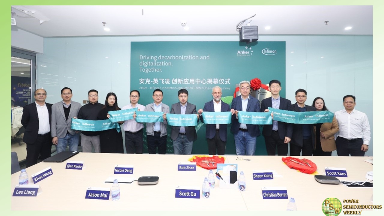
Infineon Technologies AG announced its joint Innovation Application Center in Shenzhen with Anker Innovations, a global leader in charging technology. With the center already fully operating, it is paving the way for more energy-efficient and CO2-saving charging solutions that support decarbonization.
Driven by the growing consumer demand for faster charging solutions due to an increasing usage of mobile devices, laptops and other battery-powered devices, the idea of establishing an Anker-Infineon Innovation Application Center dated back to 2021. After two years of preparation, the joint lab now serves as R&D hub for industry experts to develop power-delivery (PD) fast charging solutions with higher power density, mainly based on Infineon’s next-generation Hybrid Flyback (HFB) controller product family and the CoolGaN™ IPS for fast chargers above 100W.
Anker has already brought several successful products to the market, such as the industry-leading 100W+ fast charger device powered by Infineon’s CoolGaN in 2022. With the Innovation Application Center Anker and Infineon will even shorten the application cycle and accelerate the time to market for future products.
“Anker is an important customer for Infineon,” said Christian Burrer, Vice President of Systems & Application Marketing of Power & Sensor Systems Division at Infineon Technologies. “We have already started a strong cooperation in the charging field, with product and system solutions covering several Infineon product lines. In the field of PD charging, we provide our customers a comprehensive product portfolio, including state-of-the-art power controllers, first-class switching power supplies, leading silicon MOSFET and GaN transistor performance, and more.”
Beyond charging solutions, the joint lab is focusing on a more diversified range of consumer applications, driven by Infineon’s expertise in wide-bandgap materials such as gallium nitride (GaN). The acquisition of GaN Systems in 2023 has significantly accelerated Infineon’s GaN roadmap and further strengthens its leadership in power systems through mastery of all relevant power semiconductor technologies.
“In 2023, Anker achieved success in many markets such as China and Europe. This would not have been possible without Infineon’s GaN technology solutions and the strong collaboration between our companies. We look forward to even intensifying our partnership with Infineon”, said by Kang Xiong, General Manager of the charging business unit at Anker Technologies.
Original – Infineon Technologies
-

Qorvo® unveiled an automotive-qualified silicon carbide (SiC) field effect transistor (FET) offering an industry-best 9mΩ RDS(on) in a compact D2PAK-7L package. This 750V SiC FET is the first in a new family of pin-compatible SiC FETs from Qorvo with RDS(on) options up to 60mΩ, making them well suited for electric vehicle (EV) applications, including on-board chargers, DC/DC converters and positive temperature coefficient (PTC) heater modules.
The UJ4SC075009B7S features a 9mΩ typical RDS(on) at 25°C needed for reducing conduction losses and maximizing efficiency in high voltage, multi-kilowatt automotive applications. Its small, surface-mount package enables automated assembly flows and reduces customer manufacturing costs. This new 750V family complements Qorvo’s existing 1200V and 1700V automotive SiC FETs in D2PAK packaging to form a complete portfolio addressing EV applications that span 400V and 800V battery architectures.
Ramanan Natarajan, director of Product Line Marketing for Qorvo’s Power Products, said, “The launch of this new family of SiC FETs demonstrates our commitment to providing EV powertrain designers the most advanced and efficient solutions for their unique automotive power challenges.”
These fourth generation SiC FETs leverage Qorvo’s unique cascode circuit configuration, in which a SiC JFET is co-packaged with a Si MOSFET to produce a device with the efficiency advantages of wide bandgap switch technology and the simpler gate drive of silicon MOSFETs. Efficiency in SiC FETs is dependent on conduction losses, and Qorvo’s cascode/JFET approach enables reduced conduction losses through industry-best RDS(on) and body diode reverse voltage drop.
The key features of the UJ4SC075009B7S include:
- Threshold voltage VG(th): 4.5V (typical) allowing 0 to 15V drive
- Low body diode VFSD: 1.1V
- Maximum operating temperature: 175°C
- Excellent reverse recovery: Qrr = 338 nC
- Low gate charge: QG = 75 nC
- Automotive Electronics Council (AEC) Q101-qualified
Original – Qorvo
-
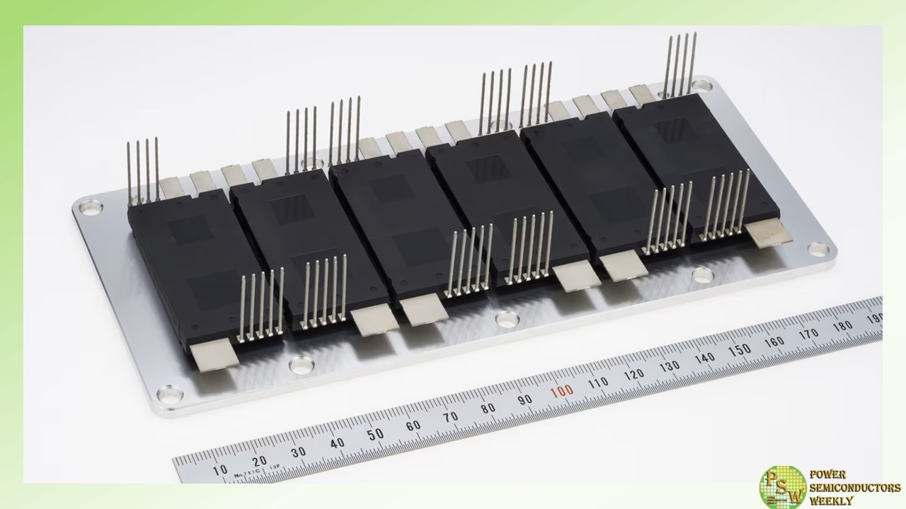
Mitsubishi Electric Corporation announced the coming release of six new J3-Series power semiconductor modules for various electric vehicles (xEVs), featuring either a silicon carbide metal-oxide semiconductor field-effect transistor (SiC-MOSFET) or a RC-IGBT (Si), with compact designs and scalability for use in the inverters of electric vehicles (EVs) and plug-in hybrid electric vehicles (PHEVs). All six J3-Series products will be available for sample shipments from March 25.
The new power modules will be exhibited at the 38th Electronics R&D, Manufacturing and Packaging Technology Expo (NEPCON JAPAN 2024) from January 24 to 26 at Tokyo Big Sight, Japan, as well as other exhibitions in North America, Europe, China and additional locations.
As power semiconductors capable of efficiently converting electricity expand and diversify in response to decarbonization initiatives, the demand is increasing for SiC power semiconductors offering significantly reduced power loss. In the xEV sector, power semiconductor modules are used widely in power conversion devices such as inverters for xEV drive motors.
In addition to extending the cruising range of xEVs, compact, high-power, high-efficiency modules are needed to further downsize batteries and inverters. But due to the high safety standards set for xEVs, power semiconductors used in drive motors must be more reliable than those used in general industrial applications.
Development of these SiC products was partially supported by Japan’s New Energy and Industrial Technology Development Organization (NEDO).
Original – Mitsubishi Electric
-

Infineon Technologies AG and Wolfspeed, Inc. announced the expansion and extension of their existing long-term 150mm silicon carbide wafer supply agreement, originally signed in February 2018. The extended partnership includes a multi-year capacity reservation agreement.
It contributes to Infineon’s general supply chain stability, also with regard to the growing demand for silicon carbide semiconductor products for automotive, solar and EV applications and energy storage systems.
“As the demand for silicon carbide devices continues to increase, we are following a multi-source strategy to secure access to a high-quality, global and long-term supply base of 150mm and 200mm SiC wafers. Our prolonged partnership with Wolfspeed further strengthens Infineon’s supply chain resilience for the coming years,” said Jochen Hanebeck, CEO of Infineon Technologies. “We have been working with Wolfspeed for more than 20 years to bring the promise of silicon carbide to the automotive, industrial and energy markets, and to help customers leverage this energy-efficient technology to foster decarbonization.”
The adoption of silicon carbide-based power solutions is rapidly growing across multiple markets. Silicon carbide solutions enable smaller, lighter and more cost-effective designs, converting energy more efficiently to unlock new clean energy applications. To better support these growing markets, Infineon is continuously diversifying its supplier base to secure access to high-quality silicon carbide substrates.
“Wolfspeed is the world’s leader in silicon carbide production. We are the catalyst in the industry transition to silicon carbide, providing high-quality materials to key customers like Infineon, a leading supplier in both the automotive and industrial markets, while also scaling our capacity footprint,” said Wolfspeed president and CEO Gregg Lowe. “Industry estimates indicate demand for silicon carbide devices, as well as the supporting material, will grow substantially through 2030, representing a $20 billion annual opportunity. We are very pleased to continue our partnership with Infineon and to serve as a major supplier of silicon carbide wafers in the years ahead.”
Original – Infineon Technologies
-
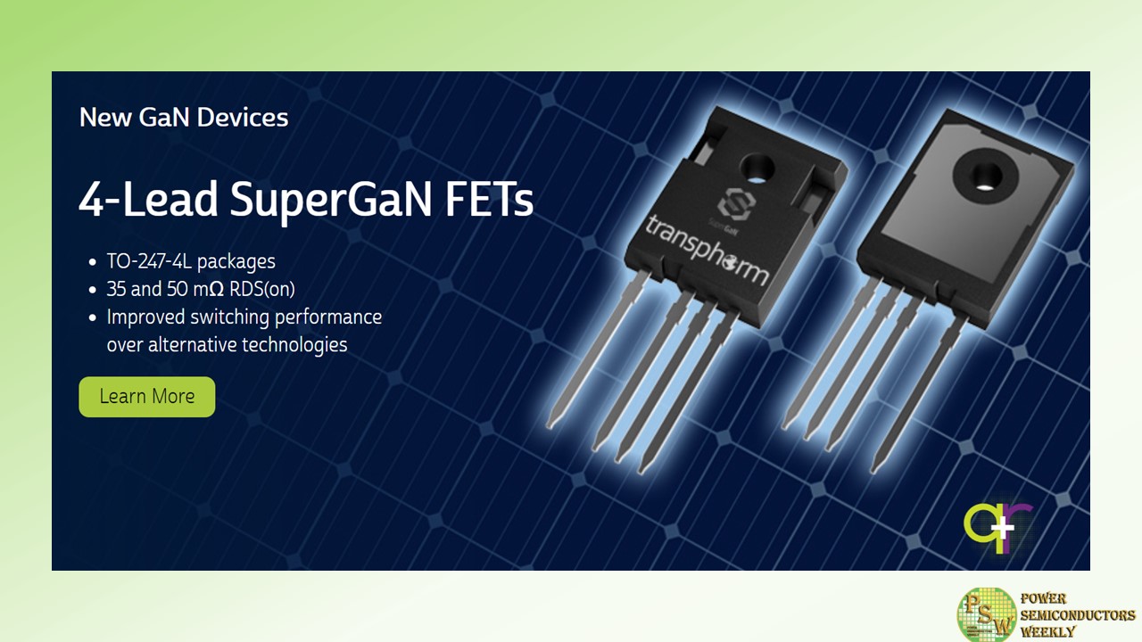
Transphorm, Inc. announced availability of two new SuperGaN® devices in a 4-lead TO-247 package (TO-247-4L). The new TP65H035G4YS and TP65H050G4YS FETs offer a 35 mOhm and 50 mOhm on resistance respectively, complete with a kelvin-source terminal that gives customers versatile switching capabilities with even lower energy losses.
The new products will run on Transphorm’s well-established GaN-on-Silicon substrate manufacturing process that is cost-effective, reliable, and well-suited for high volume manufacturing on silicon production lines. The 50 mOhm TP65H050G4YS FET is currently available while the 35mOhm TP65H035G4YS FET is sampling and slated for release in calendar Q1’2024.
Transphorm’s 4-lead SuperGaN devices can serve as an original design-in option or as a drop-in replacement for 4-lead silicon and SiC solutions supporting power supplies at 1 kilowatt and up in a wide range of data center, renewables, and broad industrial applications. As noted, the 4-lead configuration offers flexibility to users for further improved switching performance.
In a hard-switched synchronous boost converter, the 35 mOhm SuperGaN 4-lead FET reduced losses by 15 percent at 50 kilohertz (kHz) and by 27 percent at 100 kHz when compared to a SiC MOSFET device with a comparable on resistance.
Transphorm’s SuperGaN FETs are known for delivering differentiating advantages such as:
- Industry-leading robustness with a +/- 20 V gate threshold and a 4 V noise immunity.
- Easier designability by reducing the amount of circuitry required around the device.
- Easier drivability as FETs can pair with well-known, off-the shelf drivers common to silicon devices.
The TO-247-4L devices offer the same robustness, designability, and drivability with the following core specifications:
Part Number Vds (V) min Rds(on) (mΩ) typ Vth (V) typ Id (25°C) (A) max Package Variation TP65H035G4YS 650 35 3.6 46.5 Source TP65H050G4YS 650 50 4 35 Source “We continue to expand our product portfolio to bring to market GaN FETs that help customers leverage our SuperGaN platform performance advantages in whatever design requirement they may have,” said Philip Zuk, Senior Vice President, Business Development and Marketing, Transphorm.
“The four-lead TO-247 package provides flexibility for designers and customers seeking even greater power system loss reductions with little to no design modifications on silicon or silicon carbide systems. It’s an important addition to our product line as we ramp into higher power applications.”
Original – Transphorm
