-
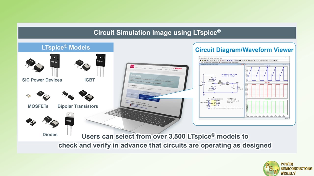
ROHM has expanded the library of SPICE model lineup for LTspice® of its circuit simulator. LTspice® is also equipped with circuit diagram capture and waveform viewer functions that make it possible for designers to check and verify in advance whether the circuit operation has been achieved as designed.
In addition to the existing lineup of bipolar transistors, diodes, and MOSFETs, ROHM has added SiC power devices and IGBTs that increases its number of LTspice® models to more than 3,500 for discretes (which can be downloaded from product pages). This brings the amount of coverage of LTspice® models on ROHM’s website to over 80% of all products – providing greater convenience to designers when using circuit simulators that incorporate discrete products, now including power devices.
In recent years, the increasing use of circuit simulation for circuit design has expanded the number of tools being utilized. Among these, LTspice® is an attractive option for a range of users, from students to even seasoned engineers at well-known companies. To support these and other users, ROHM has expanded its library of LTspice® models for discrete products.
Besides product pages, ROHM has added a Design Models page in October that allows simulation models to be downloaded directly. Documentation on how to add libraries and create symbols (schematic symbols) is also available to facilitate circuit design and simulation execution.
Going forward, ROHM will continue to contribute to solving circuit design issues by expanding the number of models compatible with various simulators while providing web tools such as ROHM Solution Simulator to meet growing customer needs.
Original – ROHM
-

Navitas Semiconductor secured the 49th position on Forbes’ 2024 America’s Successful Small Companies list. The ranking is recognition of the company’s growth based on strong demand for Navitas’ advanced, high-efficiency, wide bandgap (WBG) GaN and SiC power components, across growing and diverse global markets and an expanding customer base.
Forbes evaluated Navitas on earnings growth, sales growth, return on equity, and total stock return over the preceding five years, with a specific focus on the last 12 months, including Navitas’ 115% increase in revenue (Q3’22 to Q3’23).
Looking ahead, Navitas will host an in-person 2023 Investor Day at the company’s new Torrance HQ (with livestream), from 12:30 pm Pacific / 3:30 pm US Eastern on Tuesday 12th December. Highlights include a deep dive into four major new GaN/SiC technology platforms and focus markets, plus customer testimonials and a refresh on the $1B+ customer pipeline, plus 2024 and long-term financial outlook.
“The top 50 ranking is great recognition by Forbes for Navitas’ growth,” said Gene Sheridan, co-founder and CEO. “GaN and SiC are accelerating the transition away from fossil fuels to ‘Electrify Our World™’ with renewable sources and efficient uses of electricity. This disruptive, displacement technology upgrades from legacy silicon chips, to make existing applications more efficient, lighter, faster charging and longer range, with lower system costs.”
Original – Navitas Semiconductor
-

Efficient Energy Technology GmbH (EET), the Austrian-based pioneer in designing and producing innovative balcony power plants, has selected Efficient Power Conversion Corporation’s (EPC) EPC2204 enhancement-mode gallium nitride (eGaN®) power transistor for its latest SolMate® green solar balcony product.
The EPC2204 strikes an optimal compromise between low RDS(on) and low COSS, critical for demanding hard switching application, while featuring a drain-source breakdown voltage of 100 V in a compact package. This compact design significantly reduces PCB size, keeps current loops small, and minimizes electromagnetic interference (EMI) emissions.
EET has realized multiple benefits following the integration of GaN in its SolMate MPPT charging converter. Efficiency loss has been halved, increasing overall efficiency from 96% to 98%. The converter’s volume has decreased by 70%, the BOM and manufacturing costs have been reduced by 20%, all while lowering cooling requirements. Additionally, the increased switching frequency by a factor of 10 eliminates the need for error-prone electrolytic capacitors, thus increasing the converter’s lifespan.
By reducing power loss, EET’s system can more efficiently convert solar energy, allowing the company to generate several megawatts of additional green solar power that would otherwise dissipate as heat on a large scale. The reduced cooling requirements are particularly significant in scenarios without access to fresh air, where a water-resistant case is employed.
EET’s SolMate has won many awards for its technical innovation, for the high technical standards and the innovative design, including the James Dyson Award, Living Standards Austria, the German Sustainability Award (Design), the SolarPower Summit Award, and a finalist in the Intersolar EES Award.
Commenting on the development, Jan Senn, CMO & Sales at EET stated, “Our vision is to make renewable energy simple, safe and reliable for everyone. We accomplish this by enabling individuals to use green energy where it is most crucial – in their own homes.
SolMate combines the highest quality, excellent user experience, and design into one user-friendly lifestyle product for every home. Transitioning to GaN helps us realize this vision, and we are currently exploring the integration of GaN transistors from EPC in other power converters as well.”
Stefan Werkstetter, VP of EMEA Sales at EPC, stated, “We are delighted that EET has chosen our EPC2204 eGaN FET for their SolMate green solar balcony product. Our commitment to delivering high-performance and efficient power conversion solutions aligns perfectly with EET’s mission to make renewable energy accessible and reliable for all. We look forward to continuing our partnership with EET and contributing to the advancement of sustainable energy solutions.”
Original – Efficient Power Conversion
-
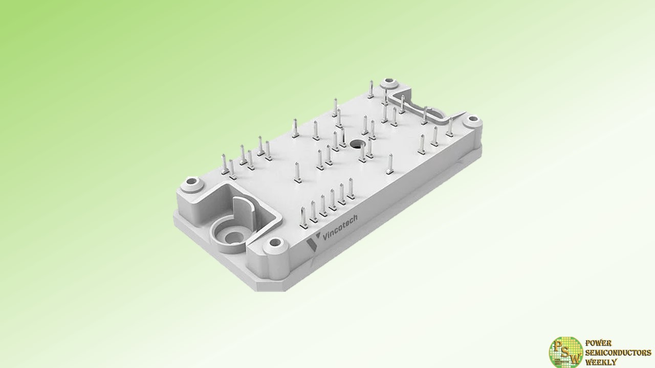
Efficiency is a big deal for heat pumps and HVAC systems that require higher power from a smaller footprint. The new Vincotech power module 1200V PIM+PFC resolves that contradiction by taking efficiency to a whole other level. Featuring a 3-phase ANPFC and an inverter stage, it enables your engineers to design more deeply integrated systems that drive costs down.
Main Benefits
- All-in-one solution: 3-phase PFC with inverter stage in a compact flow1 housing allows for more compact designs and higher power density
- AN-PFC with SiC MOSFETs and SiC diodes for up to 200 kHz: remarkably efficient topology brings down system costs
- Thin Al2O3 substrate facilitates overall thermal design
- Inverter stage featuring SiC MOSFETs for high-frequency switching
- Integrated thermal sensor simplifies temperature measurement
Applications
- Embedded Drives
- HVAC, Heatpumps
Original – Vincotech
-

Coherent Corp. announced that it has closed the $1 billion aggregate investment by DENSO CORPORATION and Mitsubishi Electric Corporation in Coherent’s silicon carbide semiconductor business.
Under the terms of the transaction announced on October 10, 2023, DENSO and Mitsubishi Electric each invested $500 million in exchange for a 12.5% non-controlling ownership interest in the Business, with Coherent owning the remaining 75%. Coherent has separated and contributed the Business to a new subsidiary that will operate the Business. Going forward, all operating and capital expenses of the Business will be funded by the Business. Coherent will control and operate the Business, which will continue to be led by Sohail Khan, Executive Vice President, Wide-Bandgap Electronics.
In connection with the transaction, the Business has entered into arm’s-length long-term supply arrangements with DENSO and Mitsubishi Electric that support their demand for 150 mm and 200 mm silicon carbide (SiC) substrates and epitaxial wafers.
“As I mentioned in October, we are excited to expand our strategic relationships with DENSO and Mitsubishi Electric to capitalize on the significant demand for silicon carbide,” said Dr. Vincent D. Mattera, Jr., Chair and CEO, Coherent.
“I believe that such a close relationship with two leaders in SiC power devices and modules is the best path forward to maximize shareholder value and position the Business for long-term growth. The investments from our strategic partners will be used to accelerate our capacity expansion plans and help sustain our leadership position, while ensuring the development of a robust and scalable supply for the rapidly growing market for SiC-based power electronics, largely driven by the explosive growth of the global electric vehicle market.”
“Through this strategic relationship with Coherent, we will secure a stable procurement of SiC wafers, which are critical for battery electric vehicles, and contribute to the realization of a carbon-neutral society by promoting the widespread adoption of BEVs in all regions around the world,” said Shinnosuke Hayashi, President & COO, Representative Member of the Board at DENSO.
Dr. Masayoshi Takemi, Executive Officer, Group President, Semiconductor & Device for Mitsubishi Electric, said, “We are pleased that this investment has been successfully completed. Going forward, we will further strengthen our collaboration with Coherent, leveraging their capabilities in development and manufacturing of SiC substrates, to achieve solid growth of our SiC power device business and contribute to a more sustainable world through decarbonization.”
When incorporated into electric vehicles and industrial infrastructure, SiC-based power electronics have demonstrated the potential to significantly reduce carbon dioxide emissions and accelerate the transition to a cleaner and more energy-efficient world.
Market estimates indicate that the SiC total addressable market will grow from $3 billion in 2022 to $21 billion in 2030, representing a 28% compound annual growth rate.
The transaction builds on Coherent’s more than two decades of demonstrated leadership in SiC materials. In recent years, the Company has aggressively invested to scale its manufacturing of 150 mm and 200 mm substrates to address this underserved market.
Over the past two years, Coherent has invested aggressively in capital and R&D for SiC. The closing of this $1 billion combined investment into the Business will accelerate the Company’s capital plans in the coming years. Specifically, the investment will fund the manufacturing expansion of the Business and, in combination with the concurrent supply agreements, enhance its position in the market.
The transaction enables Coherent to increase its available free cash flow to provide greater financial and operational flexibility to execute its capital allocation priorities, as it expects the aggregate $1 billion investment will be used to fund future capital expenditure requirements of the Business.
Original – Coherent
-
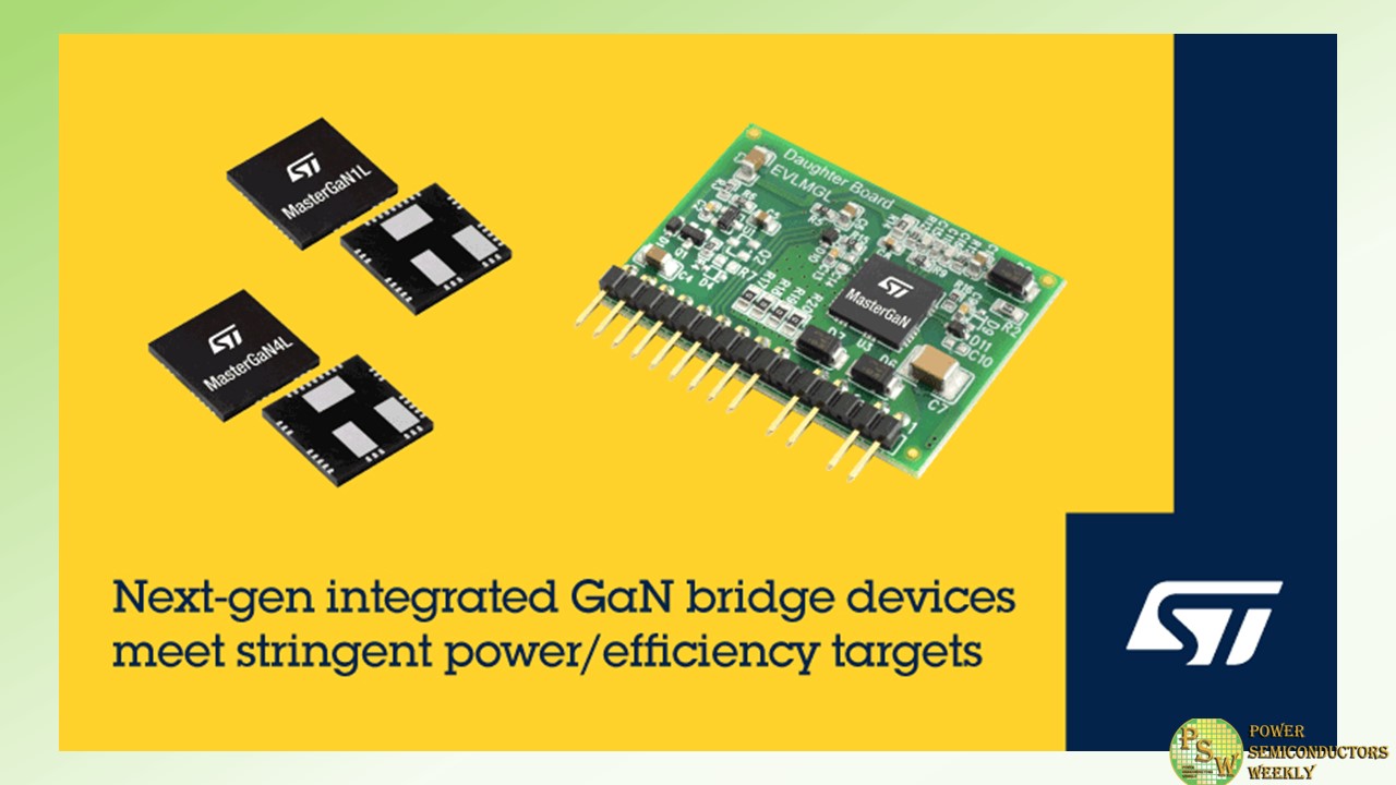
STMicroelectronics’ MasterGaN1L and MasterGaN4L introduce the next generation of integrated gallium-nitride (GaN) bridge devices that simplify power-supply design leveraging wide-bandgap technology to achieve the latest ecodesign targets.
ST’s MasterGaN family combines 650V GaN high electron-mobility transistors (HEMT) with optimized gate drivers, system protection, and an integrated bootstrap diode that helps power the device at startup. Integrating these features saves designers tackling the complex gate-drive requirements of GaN transistors. Housed in a compact power package, the devices also enhance reliability, cut the bill of materials, and ease circuit layout.
The latest devices contain two GaN HEMTs connected in half-bridge configuration. The arrangement is suitable for building switched-mode power supplies, adapters, and chargers with active-clamp flyback, active-clamp forward, and resonant converter topologies.
The MasterGaN1L and MasterGaN4L are pin compatible with MasterGaN1 and MasterGaN4 respectively. Compared to the earlier devices, they have a newly optimized turn-on delay that allows working at higher frequency and higher efficiency with low load, especially in resonant topologies.
The inputs accept signal voltages from 3.3V to 15V, with hysteresis and pull-down that facilitate connecting directly to a controlling device such as a microcontroller, DSP, or Hall-effect sensors. A dedicated shutdown pin helps designers save system power and the two GaN HEMTs have accurately matched timing with an interlocking circuit to prevent cross-conduction conditions.
The MasterGaN1L HEMTs have 150mΩ RDS(on) and 10A rated current, for use in applications up to 500W. Consuming just 20mW no-load power, and enabling high conversion efficiency, they enable designers to meet stringent industry targets for standby power and average efficiency. The MasterGaN4L HEMTs target applications up to 200W, with 225mΩ RDS(on) and rated current of 6.5A.
The EVLMG1LPBRDR1 and EVLMG4LPWRBR1 demonstration boards are available to help evaluate the features of each device. These boards contain a GaN-based half-bridge power module fine-tuned to work in an LLC application. They help quickly create new topologies leveraging the MasterGaN1L and MasterGaN4L devices without needing a complete PCB design.
Original – STMicroelectronics
-

Texas Instruments announced the expansion of its low-power gallium nitride (GaN) portfolio, designed to help improve power density, maximize system efficiency, and shrink the size of AC/DC consumer power electronics and industrial systems. TI’s overall portfolio of GaN field-effect transistors (FETs) with integrated gate drivers addresses common thermal design challenges, keeping adapters cooler while pushing more power in a smaller footprint.
“Today’s consumers want smaller, lighter and more portable power adapters that also provide fast, energy-efficient charging,” said Kannan Soundarapandian, general manager of High Voltage Power at TI.
“With the expansion of our portfolio, designers can bring the power-density benefits of low-power GaN technology to more applications that consumers use every day, such as mobile phone and laptop adapters, TV power-supply units, and USB wall outlets. Additionally, TI’s portfolio also addresses the growing demand for high efficiency and compact designs in industrial systems such as power tools and server auxiliary power supplies.”
The new portfolio of GaN FETs with integrated gate drivers, which includes the LMG3622, LMG3624 and LMG3626, offers the industry’s most accurate integrated current sensing. This functionality helps designers achieve maximum efficiency by eliminating the need for an external shunt resistor and reducing associated power losses by as much as 94% when compared to traditional current-sensing circuits used with discrete GaN and silicon FETs.
TI’s GaN FETs with integrated gate drivers enable faster switching speeds, which helps keep adapters from overheating. Designers can reach up to 94% system efficiency for <75-W AC/DC applications or above 95% system efficiency for >75-W AC/DC applications. The new devices help designers reduce the solution size of a typical 67-W power adapter by as much as 50% compared to silicon-based solutions.
The portfolio is also optimized for the most common topologies in AC/DC power conversion, such as quasi-resonant flyback, asymmetrical half bridge flyback, inductor-inductor-converter, totem-pole power factor correction and active clamp flyback.
To learn more about the benefits of TI GaN for the most common AC/DC topologies, read the technical article, “The benefits of low-power GaN in common AC/DC power topologies.”
TI has a long history of globally owned, regionally diverse internal manufacturing operations, including wafer fabs, assembly and test factories, and bump and probe facilities across 15 worldwide sites. TI has been investing in manufacturing GaN technology for more than 10 years.
With plans to manufacture more than 90% of its products internally by 2030, TI has the ability to provide customers with dependable capacity for decades to come.
Original – Texas Instruments
-

Nexperia announced its first silicon carbide (SiC) MOSFETs with the release of two 1200 V discrete devices in 3-pin TO-247 packaging with RDS(on) values of 40 mΩ and 80 mΩ. NSF040120L3A0 and NSF080120L3A0 are the first in a series of planned releases which will see Nexperia’s SiC MOSFET portfolio quickly expand to include devices with a variety of RDS(on) values in a choice of through-hole and surface mounted packages.
This release addresses the market demand for the increased availability of high performance SiC MOSFETs in industrial applications including electric vehicle (EV) charging piles, uninterruptible power supplies (UPS) and inverters for solar and energy storage systems (ESS).
“With these inaugural products, Nexperia and Mitsubishi Electric wanted to bring true innovation to a market that has been crying out for more wide-bandgap device suppliers”, according to Katrin Feurle, Senior Director & Head of Product Group SiC at Nexperia. “Nexperia can now offer SiC MOSFET devices which offer best-in-class performance across several parameters, including high RDS(on) temperature stability, low body diode voltage drop, tight threshold voltage specification as well as a very well-balanced gate charge ratio making the device safe against parasitic turn on. This is the opening chapter in our commitment to producing the highest quality SiC MOSFETs in our partnership with Mitsubishi Electric. Together we will undoubtedly push the boundaries of SiC device performance over the coming years”.
“Together with Nexperia, we’re thrilled to introduce these new SiC MOSFETs as the first product of our partnership”, says Toru Iwagami, Senior General Manger, Power Device Works, Semiconductor & Device Group in Mitsubishi Electric. “Mitsubishi Electric has accumulated superior expertise of SiC power semiconductors, and our devices deliver a unique balance of characteristics.”RDS(on) is a critical performance parameter for SiC MOSFETs as it impacts conduction power losses. Nexperia identified this as a limiting factor in the performance of many currently available SiC devices and used its innovative process technology to ensure its new SiC MOSFETs offer industry-leading temperature stability, with the nominal value of RDS(on) increasing by only 38% over an operating temperature range from 25°C to 175°C. Unlike other many currently available SiC devices in the market.
Nexperia’s SiC MOSFETs also exhibit the very low total gate charge (QG), which brings the advantage of lower gate drive losses. Furthermore, Nexperia balanced gate charge to have an exceptionally low ratio of QGD to QGS, a characteristic which increases device immunity against parasitic turn-on.
Together with the positive temperature coefficient of SiC MOSFETs, Nexperia’s SiC MOSFETs offers also ultra-low spread in device-to device threshold voltage, VGS(th), which allows very well-balanced current-carrying performance under static and dynamic conditions when devices are operated in parallel. Furthermore, low body diode forward voltage (VSD) is a parameter which increases device robustness and efficiency, while also relaxing the dead-time requirement for asynchronous rectification and free wheel operation.
Nexperia is also planning the future release of automotive grade MOSFETs. The NSF040120L3A0 and NSF080120L3A0 are available in production quantities now. Please contact Nexperia sales representatives for samples of the full SiC MOSFET offering.
Original – Nexperia
-
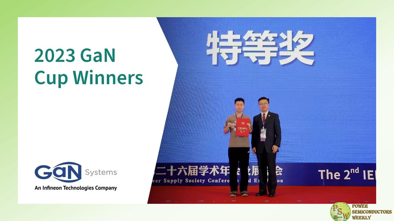
GaN Systems™, an Infineon Technologies Company, announced the winners for the 9th “GaN Systems Cup” Power Electronics Application Design Competition at the 2023 China Power Electronics and Energy Conversion Congress and the 26th China Power Supply Society Annual Conference & Exhibition (CPEEC & CPSSC 2023), taking place on November 10-13, 2023, in Guangzhou, China. The Xi’an Jiaotong University team’s three-phase inverter prototype design was recognized as the Grand Prize for achieving outstanding efficiency and power density with GaN Systems’ high-performance power transistors.
Since 2015, the Power Electronics Application Design Competition has encouraged over a thousand college students to sharpen their knowledge with practical design experience and explore possibilities in power electronics.
Participation was again unprecedented this year, with 68 teams from 48 top universities submitting project proposals. Out of the 24 teams that entered finals, 10 eventually received recognition. The Xi’an Jiaotong University team earned the Grand Prizes for their outstanding high-efficiency, high-power density three-phase inverter design. With an output power of 500W, an input voltage of 350VDC, and an output voltage of 220VAC with frequency increased from 50Hz to 400Hz and eventually 2000Hz, the team’s design delivered an impressive 15W/in3 power density and average 98% efficiency.
“The power industry is constantly looking for novel approaches to create more powerful, smaller, and faster components that increase overall system power density and efficiency,” said Yunsheng Qu, Senior Manager of Infineon’s Power and Sensor Systems Division, at the award ceremony. “GaN adoption is now at the tipping point in many applications, and developing a pipeline of skilled, talented engineers has become ever-crucial to support such massive market growth potential. I am pleased to see many of the winning entries not only meet the design requirements but go well beyond them.”
Co-located with the GaN Systems Cup, CPEEC & CPSSC 2023 drew a record-breaking 2,600 visitors and nearly 100 exhibitors, making it China’s largest academic event in power electronics. Infineon’s GaN Systems business line showcased an array of groundbreaking power system reference designs for automotive, industrial, and consumer applications. The impressively compact and economical 11kW 800V GaN-based onboard charger reference design was the main attraction in the booth. Visitors also showed a high level of interest in the implementation benefits enabled by the new Gen4 platform and responded positively to the closing of the Infineon acquisition.
Original – GaN Systems
-

AIXTRON SE enables the semiconductor foundry BelGaN to expand its business into the growing GaN marketand to accelerate GaN technology innovation. For this important strategic step, BelGaN relies on AIXTRON’s new G10-GaN, which offers best-in-class performance, an all-new compact design, and overall lowest cost per wafer.
Starting with an 8x150mm configuration, the system will be delivered to the BelGaN production site in Oudenaarde (Belgium) before the end of 2023 and will in the future migrate to 5x200mm.
BelGaN, a leading GaN (Gallium Nitride) automotive-qualified semiconductor open foundry in Europe, recently announced the production start of its first generation 650V eGaN technology. The Gen1 platform is designed for the requirements of energy-efficient applications for sustainability and carbon neutrality.
The G10-GaN will be used to further extend the range of power chips with voltage ratings from 40V to 1200V, using GaN-on-Si, GaN on SOI, and novel GaN-on-engineered substrates. It will be applied both on lateral as well as vertical power-GaN products, with a focus on high performance, automotive quality and reliability, high yield, and low costs.
“GaN-epitaxy using MOCVD is a most critical process in any power-GaN technology, both to innovate device architectures, boost performance, yield, and quality, and to cut down the cost of GaN products. This drives a paradigm shift in power electronics, opening up fast-growing markets in e-mobility, datacom, energy conversion, etc., on a road to an electrified, carbon-neutral society.
We have been impressed by the high levels of productivity, uniformity, and low cost of ownership of AIXTRON’s new G10 platform. We highly value AIXTRON’s technological advance, leadership, and continuous innovation. The proximity of AIXTRON, in the midst of the GaN ValleyTM ecosystem, and the collaboration with its team is essential for us to rapidly achieve our innovation and production objectives,” says Dr Marnix Tack, CTO and Vice President Business Development of BelGaN.
“We are very proud that BelGaN chose AIXTRON and our latest innovative powerhouse, the G10-GaN, for the important strategic milestone to add GaN epitaxy to its existing GaN processing line in Oudenaarde (Belgium). Currently, GaN power devices are rapidly adopted in a wide range of applications, and many customers are adding GaN capabilities to their silicon lines. We are excited that technology made by AIXTRON is facilitating this important transition,” says Dr. Felix Grawert, CEO and President of AIXTRON SE.
The all-new G10-GaN cluster solution builds on the fundamentals of AIXTRON’s current tool of record, the G5+ C, while extending each single performance metric:the new platform delivers twice the productivity per cleanroom area while enabling a new level of material uniformities, unlocking new levers of competitiveness for AIXTRON’s customers.
They benefit from more than 25% lowest cost of ownership than with any other equipment on the market today. The G10-GaN also guarantees the highest throughput per m2/cleanroom, and with its full automation end-to-end, it is the only MOCVD system fully designed for silicon fabs.
Original – AIXTRON
