-

Many industrial applications today are moving towards higher power levels with minimized power losses. One way to achieve this is to increase the DC link voltage. Infineon Technologies AG is addressing this market trend with the CoolSiC™ Schottky diode 2000 V G5 product family, the first discrete silicon carbide diodes with a breakdown voltage of 2000 V, introduced in September 2024.
The product portfolio has now been expanded to include a Schottky diode in the TO-247-2 package, which is pin-compatible with most existing TO-247-2 packages. The product family fits perfectly for applications with DC link voltages up to 1500 V DC, making it ideal for solar and EV chargers.
The CoolSiC Schottky diode 2000 V G5 in the TO-247-2 package is available with current ratings ranging from 10 to 80 A. It allows developers to achieve higher power levels in their applications while reducing the component count by half compared to 1200 V solutions. This simplifies the overall design and facilitates a seamless transition from multi-level to two-level topologies.
In addition, the Schottky diode in the TO-247-2 package incorporates .XT interconnection technology, which significantly reduces thermal resistance and impedance, thereby enhancing heat management. Humidity robustness has been validated through HV-H3TRB reliability testing. The diodes exhibit neither reverse recovery nor forward recovery, and feature a low forward voltage, ensuring improved system performance.
The 2000 V diode family is a perfect match for the CoolSiC MOSFETs 2000 V in the TO-247Plus-4 HCC package that Infineon launched in the spring of 2024. In addition to the TO-247-2 package, the CoolSiC Schottky Diode 2000 V is also available in the TO-247PLUS-4 HCC package.
Original – Infineon Technologies
-
NoMIS Power has announced a major breakthrough in improving the short-circuit withstand time (SCWT) of SiC MOSFETs. This innovation addresses one of the key challenges limiting the widespread adoption of SiC technology in high-power applications.
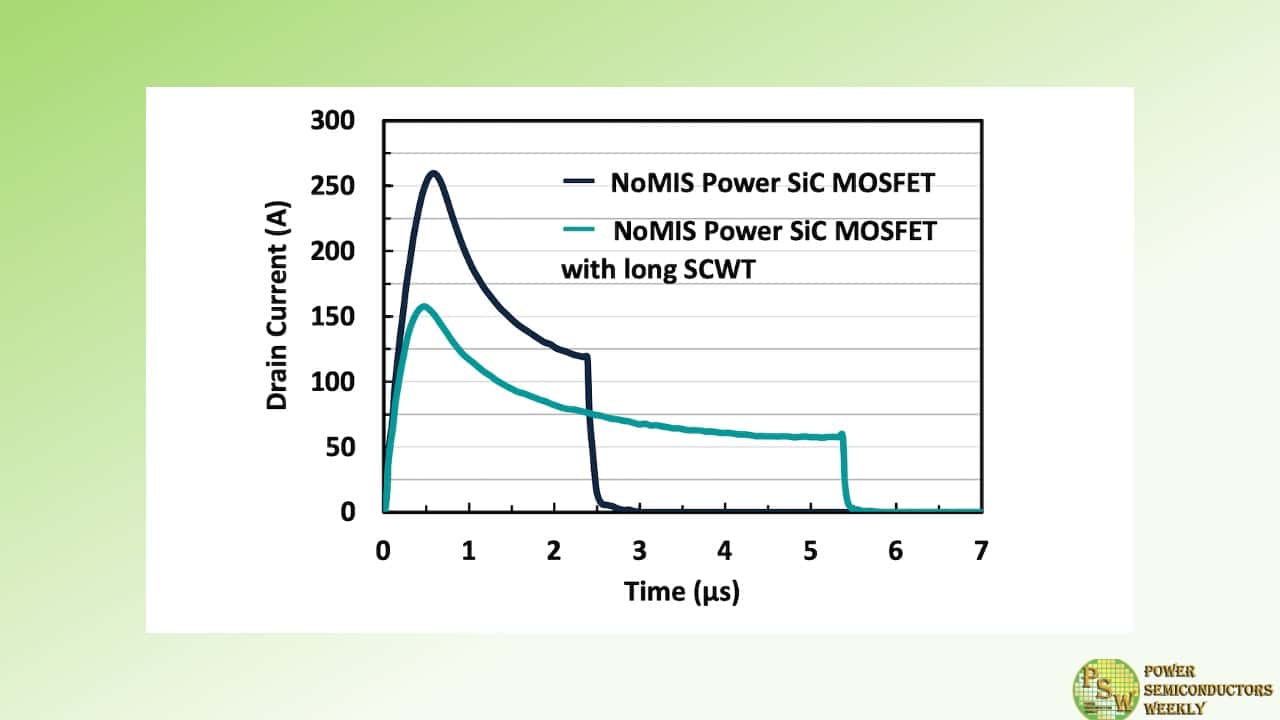
Silicon carbide (SiC) devices have gained prominence in power electronics due to their high efficiency, fast switching, and superior thermal performance. However, their historically lower short-circuit robustness compared to silicon-based IGBTs has posed challenges for their use in high-voltage and high-reliability environments, such as industrial drives, electric vehicles, and grid applications. NoMIS Power’s latest advancement significantly extends the SCWT of SiC MOSFETs to a minimum of 5 µs (Fig. 1), compared to the current industry standard of 2-3 µs, with no deleterious effect on specific on-resistance (Ron,sp) (Fig. 2). This enhancement greatly improves reliability and unlocks new opportunities for system designers seeking to maximize performance while maintaining fault tolerance.
Figure 1: Drain currents of the NoMIS Power SiC MOSFET and NoMIS Power SiC MOSFET with long SCWT under short-circuit conditions right before failure. Drain currents of the 1.2 kV, 80 mΩ SiC MOSFET (dark blue) and the long SCWT 1.2 kV, 80 mΩ SiC MOSFET (light blue) from NoMIS Power are compared. The measurement for short-circuit was conducted under the following conditions: Rg of 20 Ω, Vgs of 20 V, and a Vds of 800 V.
By tuning the trade-off between Ron,sp and SCWT using NoMIS Power’s proprietary SiC MOSFET fabrication design and process flow, the performance shown in Fig. 1 & Fig. 2 was achieved; and can be similarly managed depending on the specific application. Complete optimization of SiC MOSFETs with long SCWT using this approach will allow NoMIS Power to further extend the SCWT while maintaining negligible impact on Ron,sp.
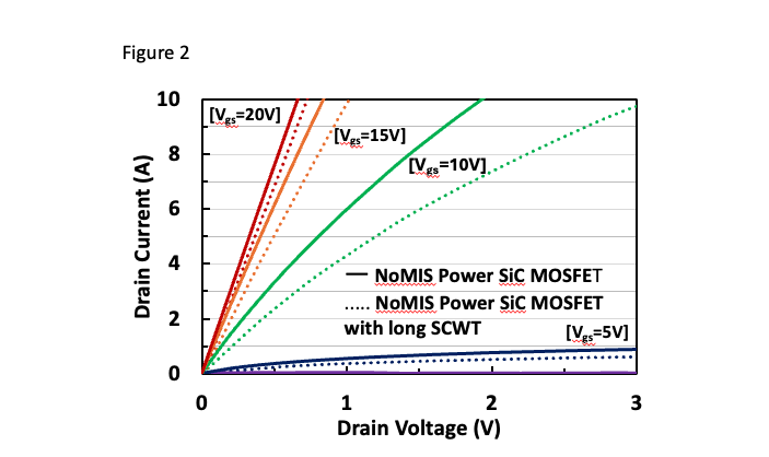
Figure 2: Typical output characteristics of NoMIS Power 1.2 kV, 80 mQ SiC MOSFET and NoMIS Power 1.2 kV, 80 mQ SiC MOSFET with long SCWT showing no significant negative impact on on-resistance.
“At NoMIS Power, we have focused extensively on device architecture engineering, leading to a significant advancement in SiC short-circuit withstand time,” said Woongje Sung, CTO at NoMIS Power. “We believe this achievement provides valuable advantages to the power electronics community, helping engineers integrate SiC solutions with greater confidence in applications where robustness is critical.”
NoMIS Power’s long SCWT devices are well-screened for latent defects and offer easier gate driver desaturation (dSat) design for high di/dt and dv/dt, enabling faster switching frequencies of up to hundreds of kHz. Initial test results demonstrate a 2X to 4X increase in short-circuit withstand time compared to existing SiC devices, positioning NoMIS Power’s technology as a frontrunner in the next generation of power semiconductors. Additionally, when coupled with packaging innovations that impact junction-to-case thermal capacitance, alongside novel thermal management techniques with high heat transfer coefficients, the overall SCWT of the SiC MOSFET can be further improved.
The impact of this innovation extends across multiple industries, including renewable energy, electric transportation, and high-power industrial applications. A longer short-circuit withstand time ensures rugged and reliable performance in critical applications, reinforcing the robustness of SiC-based power systems. For example, built-in redundancy of the SiC MOSFETs inside power converters, which impacts costs as well as power density, can be reduced. Furthermore, applications sensitive to electromagnetic inference, that cannot solely rely on digital control and sensing schemes to detect and act upon short-circuit events, will now be able to effectively utilize SiC MOSFETs with lower risk. As SiC adoption accelerates, NoMIS Power’s breakthrough will play a pivotal role in enhancing the reliability and safety of SiC-based power converters and systems.
NoMIS Power is showcasing this breakthrough technology at APEC 2025, March 16-20, Atlanta, GA, Booth 548 along with its expanded range of SiC discretes and power modules.
Original – NoMIS Power
-

Navitas Semiconductor has announced a latest breakthrough of the world’s first production-released 650 V bi-directional GaNFast ICs and high-speed isolated gate-drivers, creating a paradigm shift in power with single-stage BDS converters, which enables the transition from two-stage to single-stage topologies. Targeted applications range widely and opens up multi-billion dollar market opportunities across EV charging (On-Board Chargers (OBC) and roadside), solar inverters, energy storage and motor drives. The recorded launch event video can be viewed here.
Over 70% of today’s high-voltage power converters use a ‘two-stage’ topology. For example, a typical AC-DC EV OBC implements an initial power-factor-correction (PFC) stage and a follow-on DC-DC stage, with bulky ‘DC-link’ buffering capacitors. The resulting systems are large, lossy, and expensive. Bi-directional GaNFast consolidates the two stages into a single, high-speed, high-efficiency stage and in the process, eliminates the bulky capacitors and input inductors – the ultimate solution in EV OBCs.
A leading EV and solar micro-inverter manufacturer have already begun their implementation of single-stage BDS converters to improve efficiency, size, and cost in their systems. GaNFast-enabled single-stage converters achieve up to 10% cost savings, 20% energy savings, and up to 50% size reductions.
The ultimate power semiconductor switch (transistor) can block voltage and allow current flow in two directions, with the highest efficiency. Navitas’ leadership in GaN innovation has delivered this landmark – the bi-directional GaNFast power IC.
Previously, two discrete, ‘back-to-back’ single switches had to be used, but new bi-directional GaNFast ICs are leading-edge, single-chip designs (monolithic integration) with a merged drain structure, two gate controls, and a patented, integrated, active substrate clamp. One high-speed, high-efficiency bi-directional GaNFast IC replaces up to 4 older switches, increasing system performance while reducing component count, PCB area, and system costs.
The initial 650 V bi-directional GaNFast ICs include NV6427 (100 mΩ RSS(ON) typ.) and NV6428 (50 mΩ RSS(ON) typ) in thermally enhanced, top-side-cooled TOLT-16L (Transistor Outline Leaded Topside-cooled) packaging. The product family will be extended into lower RSS(ON) offerings in the future.
The new, high-speed IsoFast devices are galvanically isolated, high-speed drivers optimized to drive bi-directional GaN. With 4x higher transient immunity than existing drivers (up to 200 V/ns) and no external negative bias supply needed, they deliver reliable, fast, accurate power control in high-voltage systems. Initial parts are the NV1702 (dual, independent-channel, digital, isolated bi-directional GaN gate driver) and NV1701 (half-bridge GaN digital isolator) in SOIC-16N and SOIC-14W packages.
“These ICs are a truly game-changing and disruptive technology both at the semiconductor and at the system level. They not only deliver improved efficiency, power density, simplicity, and system costs but will also transform multiple multi-billion-dollar markets in the most sustainable way possible.” Gene Sheridan, CEO and co-founder of Navitas commented. “The future of our electrified planet is bi-directional energy flow. From all renewable energy sources, the power grid, and all electrified applications, such as ESS, solar and EVs, energy should flow efficiently & bi-directionally, creating a critical new currency for our future planet. Single-stage BDS converters are the key for this inflection”.
Bi-directional GaNFast ICs (NV6427 and NV6428) are fully qualified and immediately available in mass-production quantities. IsoFast (NV1701 and NV1702) samples are available now to qualified customers.
Single-stage evaluation boards and user guide showcasing both IsoFast and bi-directional GaNFast ICs are available for qualified customers.
Navitas will feature bi-directional GaNFast ICs and IsoFast at the APEC 2025 power electronics conference in Atlanta, March 17th-19th, booth 1107.
Original – Navitas Semiconductor
-

Wise-integration will unveil its latest WiseGan® and WiseWare® advancements at APEC 2025 in Atlanta, featuring two technical presentations and demonstration boards, including a new 1.5kW Totem Pole PFC module designed specifically for server and industrial applications.
“GaN technology continues to drive new efficiencies in power electronics, and APEC 2025 is the ideal platform to showcase our latest advancements,” said Thierry Bouchet, CEO of Wise-integration. “Our WiseWare® digital controllers are accelerating the adoption of GaN by enabling higher performance, system simplification, and seamless integration. Beyond efficiency, they lay the foundation for the next generation of intelligent power systems, addressing the growing demands of AI-driven server and industrial applications. These innovations are re-shaping the future of power conversion.”
Presentations
Technical Session (T04.4): “Novel Dual Output LDO Architecture in 650-V GaN Technology for Power ICs”
- Speaker: Plinio Bau, IC Design Engineer
- Date/Time: Tuesday, March 18, 9:30 – 9:50 AM
- Overview: Introduction of a novel dual-output, low-dropout regulator (LDO) architecture designed for 650-V GaN technology to enhance power IC efficiency and performance.
Industrial Session (IS26): “Comparing ZVS Losses Distribution of Similar High-Performance GaN HEMTs”
- Speaker: Theo Simon, Power Electronics Application Engineer
- Date/Time: Thursday, March 20, 11:00 – 11:25 AM
- Overview: Analysis of zero-voltage switching (ZVS) loss distribution in high-performance GaN high-electron-mobility transistors (HEMTs) to optimize power conversion efficiency.
Live Demonstrations at Booth #1238: Wise-integration will showcase four state-of-the-art boards, featuring its latest WiseWare® technologies:
- 1.5kW Single-Phase Totem Pole PFC (CrCM) – Designed for server and industrial applications, powered by WiseWare® digital control, with switching frequencies from 200 kHz to 730 kHz,
- 300W Totem Pole PFC (CrCM) – Highlights GaN’s efficiency in power conversion using the WIW1101 MCU Digital Controller and WiseGan® WI71060A,
- 300W Totem Pole PFC (CrCM)-LLC – Demonstrates improved PFC-LLC performance with WIW1101 MCU Digital Controller, WiseGan® WI71060A (PFC), and WI71120A (LLC), and
- 150W WiseWare® 2 Demo Board – Showcases a patented single-stage architecture that virtualizes power factor correction (PFC), significantly simplifying system designAbout WiseWare® Digital ControllerWiseWare® is a high-frequency digital AC-DC controller portfolio for SMPS applications. Utilizing MCU-based ZVS proprietary firmware, it optimizes GaN transistor power conversion. WiseWare® 1.1 (WIW1101) is a digital controller for Totem Pole PFC in AC-DC converters, enabling CrCM operation with ZVS to maximize efficiency.
Original – Wise-integration
-

Cambridge GaN Devices revealed more details about a solution that will enable the company to address EV powertrain applications over 100kW – a market worth over $10B – with its ICeGaN® gallium nitride (GaN) technology. Combo ICeGaN® combines smart ICeGaN HEMT ICs and IGBTs (Insulated-Gate Bipolar Transistors) in the same module or IPM, maximizing efficiency and offering a cost-effective alternative to expensive silicon carbide (SiC) solutions.
Dr GIORGIA LONGOBARDI | FOUNDER AND CEO, CGD
“Today, inverters for EV powertrains either use IGBTs which are low cost but inefficient at light load conditions, or SiC devices which are very efficient but also expensive. Our new Combo ICeGaN solution will revolutionise the EV industry by intelligently combining the benefits of GaN and silicon technologies, keeping cost low and maintaining the highest levels of efficiency which, of course, means faster charging and longer range. We are already working with Tier One automotive EV manufacturers and their supply chain partners to bring this technology advancement to the market.”The proprietary Combo ICeGaN approach uses the fact that ICeGaN and IGBT devices can be operated in a parallel architecture having similar drive voltage ranges (e.g. 0-20V) and excellent gate robustness. In operation, the ICeGaN switch is very efficient, with low conduction and low switching losses at relatively low currents (light load), while the IGBT is dominant at relatively high currents (towards full load or during surge conditions).
Combo ICeGaN also benefits from the high saturation currents and the avalanche clamping capability of IGBTs and the very efficient switching of ICeGaN. At higher temperatures, the bipolar component of the IGBT will start to conduct at lower on-state voltages, supplementing the loss of current in the ICeGaN. Conversely, at lower temperatures, ICeGaN will take more current. Sensing and protection functions are intelligently managed to optimally drive the Combo ICeGaN and enhance the Safe Operating Area (SOA) of both ICeGaN and IGBT devices.
ICeGaN technology allows EV engineers to enjoy GaN’s benefits in DC-to-DC converters, on-board chargers and potentially traction inverters. Combo ICeGaN further extends the benefits of CGD’s GaN technology into the rich 100kW+ traction inverter market. ICeGaN ICs have been proven to be very robust and IGBTs have a long and proven track record in traction and EV applications. Similar, proprietary parallel combinations of ICeGaN devices with SiC MOSFETs have also been proven by CGD, but Combo ICeGaN – which is now detailed in a published IEDM paper – is a far more economical solution. CGD expects to have working demos of Combo ICeGaN at the end of this year.
Prof. FLORIN UDREA | FOUNDER AND CTO, CGD
“Having worked for three decades in the field of power devices, this is the first time I have encountered such a beautifully complementary technology pairing. ICeGaN is extremely fast and a star performer at light load conditions while the IGBT brings great benefits during full load, surge conditions and at high temperatures. ICeGaN provides on-chip intelligence while the IGBT provides avalanche capability. They both embrace silicon substrates which come with cost, infrastructure and manufacturability advantages.”CGD will be exhibiting at APEC (Applied Power Electronics Conference and Exposition). For more details about Combo ICeGaN, visit Booth 2039 at the Georgia World Congress Center | Atlanta, GA | March 16-20, 2025.
Original – Cambridge GaN Devices
-

ALLOS Semiconductors and Canadian specialty semiconductor and performance materials supplier 5N Plus Inc. have announced the acquisition of the GaN IP portfolio from 5N Plus’ subsidiary AZUR Space Solar Power.
This strategic acquisition includes the buy-back of the GaN-on-Si technology for high power electronics (HPE) applications, which was originally sold to AZUR in 2020, along with several jointly completed innovations and resulting patent applications. With this acquisition, the global IP portfolio has expanded to over 50 granted patents, with more to come, most of them essential for both GaN-on-Si for optoelectronics and HPE applications. The transaction also includes the return of all recipes and other know-how.
This acquisition strengthens ALLOS’ position in the rapidly evolving areas of micro-LED displays and optical interconnect. ALLOS’ GaN-on-Si epiwafers are crucial for the customers to utilize standard silicon fabs for micro-LED manufacturing.
Additionally, this acquisition provides ALLOS’ with the option to re-enter the GaN-on-Si high power electronics (HPE) market. Power GaN has become a global mass market success and is projected to grow to over two billion USD by 2029. The unique features of ALLOS’ 200 mm and 300 mm technology can significantly benefit in scaling up production while reducing unit costs. In addition to standard silicon fab compatibility, these features include highest crystal quality, best wafer uniformity, and award-winning breakdown voltages for undoped GaN. While ALLOS remains focused on micro-LEDs, the company is now open to collaborations with HPE players.
Original – ALLOS Semiconductors
-

Cambridge GaN Devices will demonstrate at APEC that the company’s ICeGaN® GaN ICs can now satisfy a broad range of applications with higher power requirements, such as servers, data centres, inverters, industrial power supplies and, very soon, automotive EVs over100 kW. The company’s new P2 series ICs feature RDS(on) levels down to 25 mΩ, supporting multi kW power levels with the highest efficiency, and a secure supply chain is in place including manufacturing deals with TSMC and ASE, and distribution through Digi-Key.
HENRYK DABROWSKI | SENIOR VICE PRESIDENT OF GLOBAL SALES, CGD
“GaN is now widely accepted as the technology of choice for mobile device chargers and is now set to supersede traditional silicon MOSFETs in higher power applications. The industry is also beginning to realize that GaN may replace SiC in certain high efficiency designs, due to its lower manufacturing cost. At APEC – one of the world’s most important events for the power industry – we are eagerly looking forward to having in-depth discussions with designers of high efficiency power systems and demonstrating the ruggedness, reliability and ease of use of our ICeGaN® GaN IC technology.”
During APEC, CGD will give the following Industry Session and Exhibitor Presentations:
Unlocking the Potential of Multi-level Inverters with Integrated ICeGaN technologies (Session: IS14.7)
As the electric vehicle market develops, there is a continuous drive to look at new and novel approaches to further improve the efficiency of the traction inverter and other electrical subsystems.Multi-level inverters enable the use of much high switching frequencies and break down the total voltage into smaller steps, which in turn allows for improved efficiency and downsizing of other parts of the system. GaN technology optimizes the benefits of multi-level topologies. CGD’s ICeGaN technology brings a higher level of integration, lower cost, best in class robustness and ease of use.
Presenter: Daniel Murphy, Director of Technical Marketing, CGD Date: Wednesday March 19, 2025 Time: 4:30 PM – 4:55 PM ET Location: Level Four, A411
ICeGaN Leads the Industry in GaN Integration
This presentation will demonstrate how ICeGaN technology leads in simplification, cost reduction, robustness, carbon footprint and efficiency of GaN power applications.Presenter: Peter Di Maso, Vice President, Business Development, CGD Date: Wednesday, March 19, 2025 Time: 12:45 PM – 1:15 PM ET Location: A301
On booth 2039, CGD will present demos that highlight the benefits of employing its ICeGaN technology in three application spaces: Motor Drives
- ICeGaN vs discrete GaN circuits comparison in half-bridge (daughter cards) demo board
- High and low power QORVO motor drive evaluation kits utilising ICeGaN and developed in collaboration with CGD
- Half-bridge built using CGD’s ICeGaN ICs in the BHDFN (Bottom Heat-spreader DFN) bottom-side cooled package with wettable flanks for easy inspection
Data Centres
- 3 kW totem-pole PFC evaluation board
- Half-bridge built using CGD’s BHDFN-packaged ICeGaN ICs
- Full-bridge demo showing CGD’s ICeGaN ICs in the DHDFN (Dual Heat-spreader DFN) package which has low thermal resistance (Rth(JC)), and can be operated with bottom-side, top-side and dual-side cooling. This package offers flexibility in design and out-performs the often-used TOLT package in top-side and, especially, dual-side cooled configurations.
- 2.5kW GaN-based CCM totem-pole PFC reference design targetting LED drivers, industrial brick DC/DC and general PSUs with power range of 500W to 1.5kW.
Scalable Power
- New single IC ICeGaN technology platform that delivers over 100kW, enabling CGD to address the $10B+ EV market, currently dominated by SiC, with cost-effective GaN solutions
- Single leg of a 3-phase 800 V automotive inverter demo board, developed in partnership with French public R&I institute, IFP Energies nouvelles (IFPEN)
- Parallel evaluation board demoing ICeGaN’s higher power capabilities
- Full-bridge demo showing CGD’s ICeGaN ICs in the DHDFN package
GIORGIA LONGOBARDI | FOUNDER AND CEO, CGD
“This is an exciting time for our industry as it embraces the disruptive GaN technology. Although this change from silicon has indisputably shown the power density and efficiency benefits of GaN, only CGD is presenting this new technology in an easy-to-use solution, which has been proven to be the most rugged in the industry. With our technology roadmap which details how ICeGaN will be able to address even EV applications over 100kW, we are sure designers will be inspired by the possibilities that ICeGaN has opened up.”
Original – Cambridge GaN Devices
-

ROHM has announced that the EcoGaN™ series of 650V GaN HEMTs in the TOLL package has been adopted for AI server power supplies by Murata Power Solutions, a subsidiary of the Murata Manufacturing Group and a leading supplier of electronic components, batteries and power supplies in Japan. Integrating ROHM’s GaN HEMTs, which combine low loss operation with high-speed switching performance, in Murata Power Solutions’ 5.5kW AI server power supply unit achieves greater efficiency and miniaturization. Mass production of this power supply unit is set to begin in 2025.
Rapid advancements in IoT-related fields such as AI and AR (Augmented Reality) have led to a surge in global data traffic in recent years. Notably, the power consumption for a single AI-generated response is estimated to be several times higher than that of a standard Internet search, highlighting the need for more efficient AI power supplies. Meanwhile, GaN devices, known for low ON resistance and high-speed switching performance, are gaining attention for their ability to enhance power supply efficiency while reducing the size of peripheral components such as inductors used in power circuits.
Dr. Joe Liu, Technical Fellow, Murata Power Solutions
“We are pleased to have successfully designed AI server power supply units featuring higher efficiency and power density by incorporating ROHM’s GaN HEMTs. The high-speed switching capability, low parasitic capacitance, and zero reverse recovery characteristics of GaN HEMTs help minimize switching losses. This allows for higher operating frequencies in switching converters, reducing the size of magnetic components. ROHM’s GaN HEMTs deliver competitive performance and exceptional reliability, yielding excellent results in the development of Murata Power Solutions’ 5.5kW AI server power supply units. Going forward, we will continue our collaboration with ROHM, a leader in power semiconductors, to improve the efficiency of power supplies and address the social issue of increasing power demand.”
Yuhei Yamaguchi, General Manager, Power Stage Product Development Div., LSI Business Unit, ROHM Co., Ltd.
“We are delighted that ROHM’s EcoGaN™ products have been integrated into AI server power supply units from Murata Power Solutions, a global leader in power supplies. The GaN HEMTs used in this application provide industry-leading switching performance in a high heat dissipation TOLL package, enhancing power density and efficiency in Murata Power Solutions’ power supply units. We look forward to strengthening our partnership with Murata Manufacturing, a company that shares the similar vision of contributing to society through electronics – promoting the miniaturization and efficiency of power supplies to enrich people’s lives.”
Original – ROHM
-

Leapers Semiconductor has officially commenced construction of its automotive-grade third-generation power semiconductor module project in Jiangdu District’s development zone. The launch event was part of Jiangdu District’s Major Project Construction Mobilization Conference, where local officials outlined key economic initiatives for the region. District Party Secretary Zhu Lili delivered a speech at the ceremony, emphasizing the urgency of driving economic growth from the start of the year. District Mayor Shen Bohong presided over the event, with key government representatives also in attendance.
During the event, township leaders provided updates on the district’s 2025 major construction projects, reaffirming their commitment to economic development. The first quarter alone saw the initiation of 29 major projects, with a total investment of 8.72 billion yuan ($1.2 billion), spanning sectors such as new materials, renewable energy, high-end equipment, and environmental protection.
Leapers Semiconductor SiC module project, which began construction on March 1, represents a 10 billion yuan ($1.4 billion) investment, covering an area of 32 acres. Once completed, the facility is expected to achieve an annual production capacity of 3 million automotive-grade SiC modules, generate 10 billion yuan ($1.4 billion) in annual revenue, and contribute 500 million yuan ($70 million) in annual tax revenue.
With this new SiC module packaging and testing facility, Leapers Semiconductor is set to enhance production capabilities, accelerate innovation, and drive the adoption of SiC power solutions worldwide.
Original – Leapers Semiconductor
-
 LATEST NEWS / PRODUCT & TECHNOLOGY / PROJECTS / SiC / TOP STORIES / WBG
February 27, 2025
4 Min ReadSilicon carbide (SiC) provides considerable technical advantages for power electronics – however, the costs are still a drawback. In the »ThinSiCPower« research project, a consortium of Fraunhofer Institutes is developing key technologies to reduce material losses and device thickness while increasing the thermomechanical stability of the assembled SiC chips. The savings achieved are expected to help further accelerate the market development of efficient SiC power electronics.
Power electronics based on the wide-bandgap semiconductor silicon carbide (SiC) are a key enabler for energy-efficient, sustainable and high-performance applications in electromobility – from cars and commercial vehicles to trains, ships and airplanes, in the generation, transportation and storage of renewable energies, as well as for IT and industrial infrastructures. It is therefore an important and competitively relevant factor for the current global transformation processes in the areas of mobility, energy and digitalization. The market for SiC power devices is expected to grow at an annual rate of over 30 percent. Compared to conventional silicon technology, the use of SiC power electronics in a standard drive converter saves more energy than is required to manufacture the SiC power electronics themselves.
While the technological advantages of SiC are obvious due to its physical properties, the higher costs compared to the established silicon are still an obstacle to faster market penetration. Chip costs are more than three times higher than for silicon. The initially required SiC wafer is the biggest cost driver here. In the case of a SiC-based metal-oxide semiconductor field-effect transistor (MOSFET), this accounts for more than 40 percent of the manufacturing costs. In addition, due to the unfavorable mechanical material properties and large thickness of the monocrystalline SiC wafer, electronics processed from it only achieve approx. 30 percent of the thermomechanical service life compared to silicon. This disadvantage leads to an approx. 25 percent larger chip area and, in the case of an inverter for example, to around 25 percent higher costs in the application.
In the three-year ThinSiCPower project (2024-2027), funded by the Fraunhofer PREPARE program, researchers are developing an alternative way to produce cost-effective SiC substrates and significantly thinner SiC chips using more resource-efficient processing technologies. Rather than first sawing the expensive, high-quality SiC wafers with the usual material loss and later back-grinding them in device processing, the SiC crystal is separated directly into thinner wafers using a special laser process without any major loss of material, which are then bonded onto an inexpensive carrier substrate based on polycrystalline SiC.
Fraunhofer ISE, ENAS and IWM with the Fraunhofer IISB as project coordinator are pooling their individual competencies in ThinSiCPower. A SiC coating technology developed by Fraunhofer IISB is being adapted for the manufacturing of the poly-SiC carrier substrates, which is more cost- and resource-efficient than the conventional manufacturing method using chemical vapor deposition. The low-loss separation of the thin SiC wafers is carried out using a laser for defined mechanical pre-damage (Fraunhofer ISE) and subsequent separation under well-defined mechanical conditions for controlled crack propagation (Fraunhofer IWM).
The wafer bonding process for the poly-SiC substrate with the split SiC, including the necessary surface preparation before and after the bonding process, will be developed at Fraunhofer ENAS, while the subsequent device processing and qualification will take place at Fraunhofer IISB. The partners are also developing adapted electrical test methods at thin wafer level as well as physics-of-failure simulation models to maximize the market acceptance of this new class of low-cost SiC substrates. With this, a broad applicability in the relevant industries could be achieved.
The aim is to reduce SiC device costs by 25 percent by developing technology for the production of costeffective thin SiC wafers and poly-SiC substrates. In addition, SiC design costs are to be reduced by further 25 percent by increasing the load cycle stability by 300 percent. The target markets are semiconductor and power module manufacturers as well as their process and equipment suppliers through to test equipment suppliers. With this project, the participating partner institutes are also combining their expertise to set up a complete, highly innovative and future-oriented SiC processing line within the Research Fab Microelectronics Germany (FMD). The consortium is receiving consultancy support directly from partners in industry.
The ThinSiCPower project not only accelerates the market penetration of silicon carbide through the targeted cost reduction and conceptual advantages, but also serves to secure an innovative, resilient and industry relevant SiC technology value chain in Germany and Europe.
Original – Fraunhofer IISB
