-

Soitec opened its new plant in Bernin, near Grenoble, in the presence of Thierry Breton, European Commissioner for the Internal Market and Roland Lescure, French Minister Delegate for Industry.
Soitec has developed its SmartSiC™ technology as a response to vehicle electrification challenges.
The technology, based on silicon carbide (SiC), sets a new standard with improved efficiency for energy conversion systems. Thanks to its reduced energy losses, better thermal management and improved power density, the material increases the range and performance of electric vehicles.
Through the application of SmartCut™ technology, each SiC substrate can be used 10 times.
As a result, SmartSiC™ enables electric vehicles to achieve ranges above 500 km, compared with an average 350 km for vehicles using silicon IGBT alternatives – while also reducing CO2 emissions during wafer manufacturing by 70% compared to monocrystalline SiC substrates.
Development of the technology began in 2020 in partnership with CEA-Leti and has received financial support from the French state, the region, local authorities and the European Union.
A new production facility in step with Soitec’s ambition
The new plant will have a 2,500 m2 footprint and a final production capacity of 500,000 SmartSiC™ wafers per year.
It will contribute to Soitec’s strategy of sustainable growth towards a threefold expansion of addressable markets by 2030, reinforcing the company’s leadership position in the strategic semiconductor materials market.
The new plant will lead to the creation of 400 direct jobs, while also reinforcing the attractiveness and dynamism of the “French Silicon Valley” ecosystem.
Pierre Barnabé, Chief Executive Officer of Soitec, stated: “More than ever we are ready to establish our SmartSiC™ technology as a new standard in semiconductor materials for coming generations of electric cars. This plant will enable us to meet growing demand for silicon carbide and achieve a 30% market share by 2030, while helping to make electric mobility more efficient and affordable. Completed in record time, it is the embodiment of our industrial performance and our future-facing strategy, based on the expansion of our product and technology portfolio.
This is also an important day for our region, which is once again showing its dynamic and exemplary approach to industrial innovation, with technologies designed, developed, and manufactured within our ecosystem. We will create jobs and continue to showcase French and European knowhow in global semiconductor markets.”
Original – Soitec
-

GaN Systems announced the introduction of its groundbreaking 4th generation GaN power platform. This state-of-the-art technology sets a new power efficiency and compactness standard, delivering an impressive step-function performance boost and industry-leading figures of merit. For example, with GaN Systems Gen4 in an artificial intelligence (AI) server rack, 3.2kW power supplies at 100W/in3 in 2022 are now achieving 120W/in3 with efficiencies above Titanium levels. Gen4 will revolutionize power markets, including consumer electronics, data centers, solar energy, industrial applications, and automotive.
The Gen4 platform also delivers more total bill of material cost savings compared to traditional Silicon and Silicon Carbide solutions, making GaN Systems’ technology a powerful choice for businesses seeking to enhance their competitive advantage.
“Our lead customers have already realized the benefits of our Gen4 platform,” stated Jim Witham, CEO of GaN Systems. “This platform is a testament to our ongoing commitment to continuously delivering superior performance advantages and next-generation levels of efficiency. GaN Systems, in strategic collaboration with industry leaders like TSMC, has invested significantly to meet the ever-evolving demands of our customers. We are pioneering a transformation in product offerings, packaging innovations, enriched functionalities, and unparalleled performance across our markets.”
A Huge Leap for Power Electronics Technology
The Gen4 power platform boasts the following benefits:
- >20% improvement in input and output figures-of-merit translates into reduced losses, enhanced efficiency, and more cost-effective solutions.
- Increased granularity in device specification, combined with a wide range of packaging options, including PDFN, TOLL, TOLT, and Embedded – allowing the correct Rds resistance and package combination for each application, consequently optimizing electrical and thermal system performance.
- 700V E-mode with the industry’s highest transient voltage rating, 850V, significantly enhancing total system reliability and robustness. This rating enables the semiconductor components to withstand user environment anomalies, such as voltage spikes, ensuring uninterrupted and dependable performance.
- On-state resistance ranges enable power systems from 20W to 25,000W.
For more information, visit https://gansystems.com/gan-transistors/gen-4/
Original – GaN Systems
-

Researchers at the Indian Institute of Science (IISc) have developed a fully indigenous gallium nitride (GaN) power switch that can have potential applications in systems like power converters for electric vehicles and laptops, as well as in wireless communications. The entire process of building the switch – from material growth to device fabrication to packaging – was developed in-house at the Centre for Nano Science and Engineering (CeNSE), IISc.
Due to their high performance and efficiency, GaN transistors are poised to replace traditional silicon-based transistors as the building blocks in many electronic devices, such as ultrafast chargers for electric vehicles, phones and laptops, as well as space and military applications such as radar.
“It is a very promising and disruptive technology,” says Digbijoy Nath, Associate Professor at CeNSE and corresponding author of the study published in Microelectronic Engineering. “But the material and devices are heavily import-restricted … We don’t have gallium nitride wafer production capability at commercial scale in India yet.” The know-how of manufacturing these devices is also a heavily-guarded secret with few studies published on the details of the processes involved, he adds.
Power switches are used to control the flow of power to – essentially turn on or off – electronic devices. To design the GaN power switch, the IISc team used a metal organic chemical vapour deposition technique developed and optimised over a decade by researchers in the lab of Srinivasan Raghavan, Professor and Chair, CeNSE. It involves growing GaN alloy crystals layer by layer on a two-inch silicon wafer to fabricate a multi-layered transistor.
The entire process needs to be carried out carefully in a clean room to ensure that no defects arise due to environmental conditions like humidity or temperature, which can affect device performance. The team also took the help of Kaushik Basu, Associate Professor in the Department of Electrical Engineering (EE), and his lab, to build an electrical circuit using these transistors and test their switching performance.
GaN transistors typically operate in what is called a “depletion mode” – they are on all the time unless a negative voltage is applied to turn them off. But power switches used in chargers and adapters need to work the other way around – they normally need to be off and not carrying current, and should only turn on when a positive voltage is applied (“enhancement mode”). To achieve this operation, the team combined the GaN transistor with a commercially available silicon transistor to keep the device normally off.
“The packaging of the device was also indigenously developed,” explains Rijo Baby, PhD student at CeNSE and first author of the study. After packaging and testing, the team found the device performance to be comparable to state-of-the-art switches available commercially, with a switching time of about 50 nanoseconds between on and off operations.
Going forward, the researchers plan on scaling up the device dimensions so that it can operate at high currents. They also plan to design a power converter that can step up or step down voltages.
“If you look at strategic organisations in India, they have a hard time procuring GaN transistors … It is impossible to import them beyond a certain quantity or power/frequency rating,” says Nath. “This is essentially a demonstration of indigenous GaN technology development.”
Original – Indian Institute of Science (IISc)
-
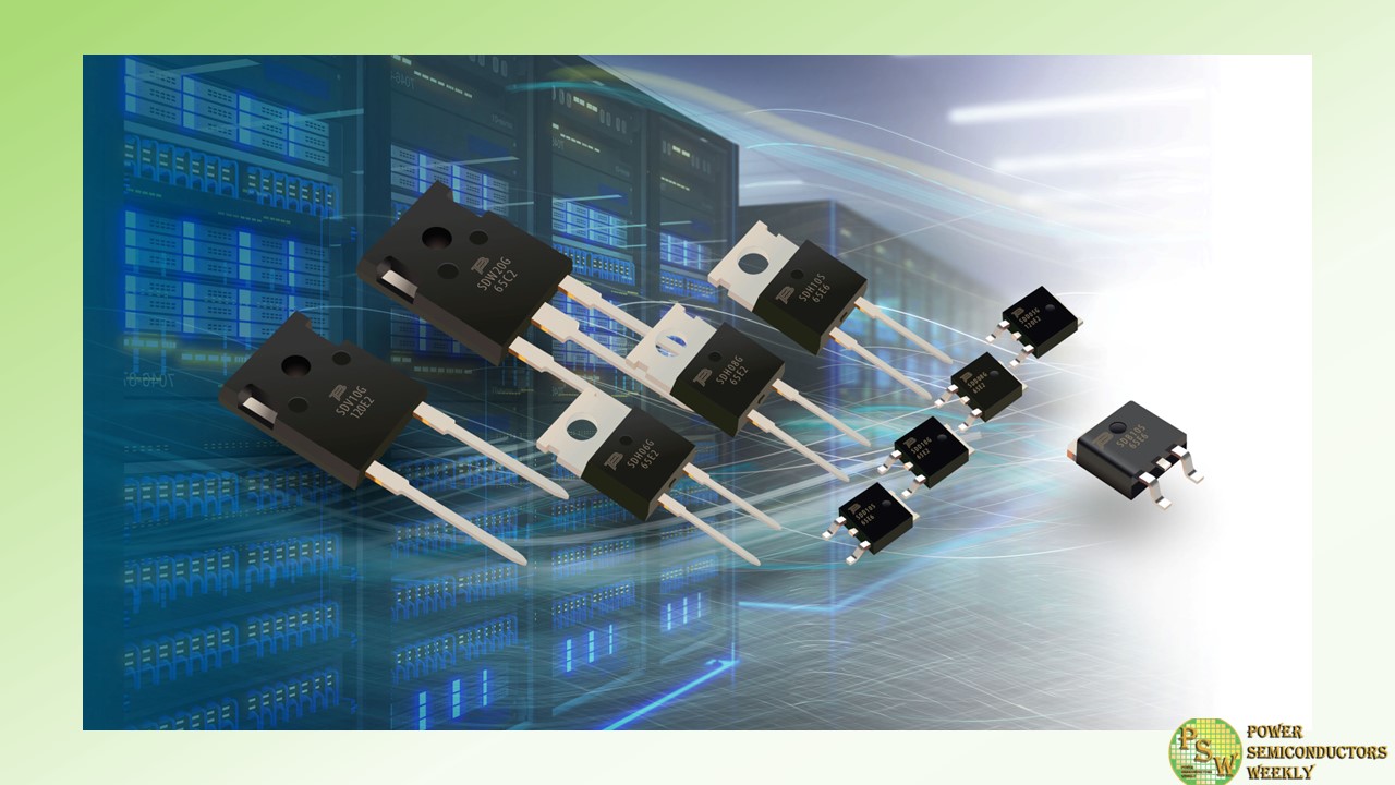
Bourns, Inc. has expanded its 650 and 1200 V Silicon Carbide (SiC) Schottky Barrier Diode (SBD) product family with 10 new models. The 10 new models added to the Bourns® SiC SBD line are designed to address the increasing power density requirements in the latest transportation, renewable energy and industrial systems.
Bourns’ expanded wide band gap diode line delivers the peak forward surge, low forward drop, reduced thermal resistance and low power loss capabilities demanded by today’s high frequency and high current applications. These capabilities also help designers develop smaller, cost-efficient and state-of-the-art power electronics.
As optimal power conversion solutions for DC-DC and AC-DC converters, Switched-Mode Power Supplies (SMPS), photovoltaic inverters, motor drives and other rectification applications, the 10 new models feature currents in the 5-10 A range, with no reverse recovery current to reduce EMI.
This enables them to significantly lower energy losses and further increase efficiency, switching performance and reliability. In addition to providing excellent thermal performance, Bourns’ new SiC SBD models are available in multiple forward voltage, current and package options that include TO220-2, TO247-3, TO252, TO263 and TO247-2.
The 10 new Bourns® BSD SiC SBD models are available now. These models are RoHS compliant, halogen free, Pb free and their epoxy potting compound is flame retardant to the UL 94V-0 standard. For more detailed product information, please see: www.bourns.com/products/diodes/silicon-carbide-sic-schottky-barrier-diodes.
Original – Bourns
-
During the past decade combination “silicon carbide” or more often “SiC” has become very popular in the world of power electronics. Many companies have started to evaluate the possibility of using SiC instead of Si in their projects. As many say, silicon carbide is here to replace silicon, and they might be right considering that SiC MOSFETs used in power semiconductor devices bring numerous advantages compared with their silicon counterparts.
SiC has a higher critical breakdown field and thermal conductivity and, a wider bandgap, which leads to lower energy losses, a lower leakage current at higher temperatures. Besides, SiC can operate at much higher frequencies. On a system level, it means using less additional components, better thermal management, and an overall smaller footprint.
This is one of the reasons why today automotive Tier-1 and OEM companies prefer to use SiC for their new projects in vehicle electrification. With SiC they can get the same efficiency with several times smaller package. For the electric car size and weight of power electronics systems are critical.
Working in the power semiconductors industry for many years, with Si and SiC power devices in particular, I see that the number of companies and end applications adopting silicon carbide is growing fast. Even though SiC is quite a young technology, and the first commercial SiC power MOSFET dates back to 2011, nowadays, we already have over ten SiC power device vendors who deliver high-quality products used in electric vehicles, solar inverters, public transportation, welding equipment, marine, medical and aerospace.
With the number of new SiC fabs and production expansions announced during the past three years it is clear that silicon carbide technology is here to stay, and here to grow further. Many analytical agencies predict that the total SiC market will reach 10 billion USD by 2030 or even earlier. And despite the fact that in volume SiC power semiconductors market still lags behind silicon. It grows faster, quite faster than expected several years ago.
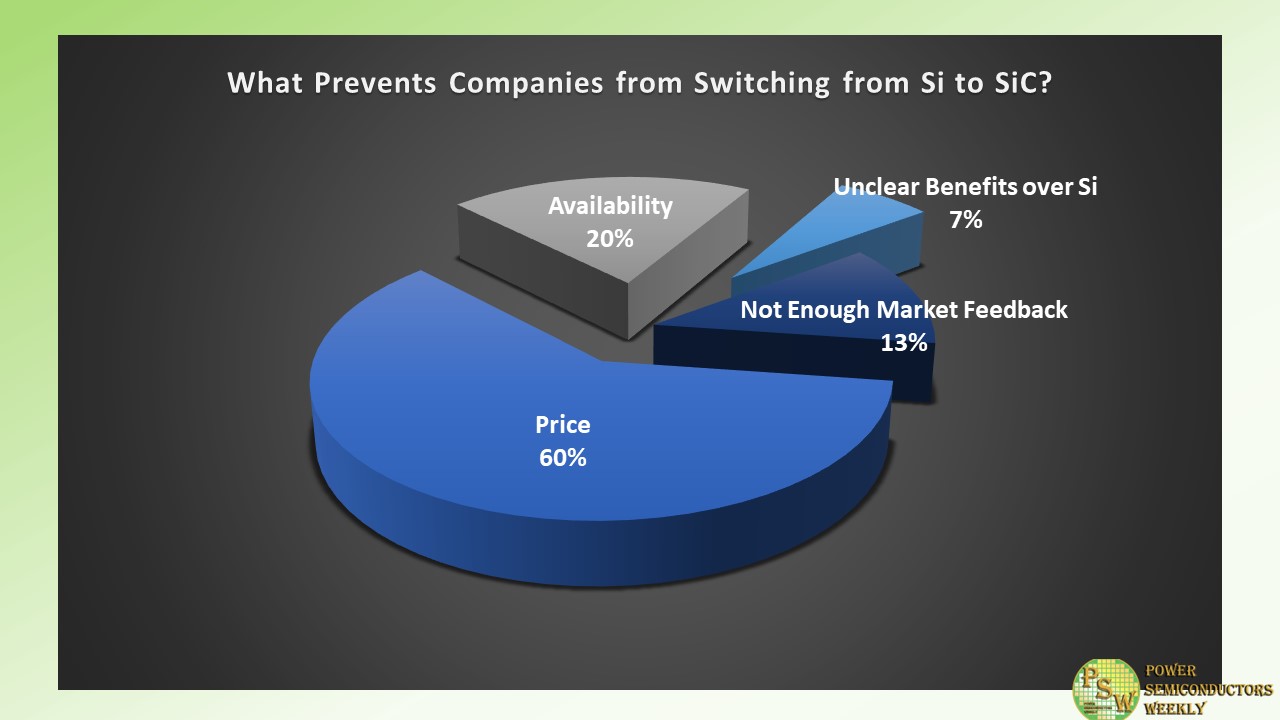
Despite the fast growth and penetration into the power electronics market, many companies still feel uncomfortable when they hear about silicon carbide and the benefits it has. During numerous negotiations and talks with the companies using power semiconductor devices, I shortlisted the most common barriers preventing them from switching from silicon to silicon carbide, or from increasing the number of SiC-based projects they already have.
To further scale this data, recently I had a poll on LinkedIn within the power electronics community. A similar poll I ran during the latest EPE’23 ECCE Europe Conference, which was held in Aalborg, Denmark. Both polls’ participants come from power semiconductors companies or from companies using power semiconductors.
Combined poll results look like this:
- Price – 60%
- Availability – 20%
- Unclear benefits over Si – 7%
- Not enough market feedback – 13%
It is clear that price is still the major concern and barrier. Even though the price has tremendously decreased during the past ten years, it remains one of the key factors why many companies prefer to use Si-based semiconductors.
The availability of SiC wafers or SiC-based devices accounts for another 20% of doubts coming from the end users. The lead time of SiC has been discussed many times, and the situation for many stays unclear. And it is the same for the remaining 20% of poll results coming from unclear benefits of SiC and lack of market feedback. Silicon power devices have been in use for decades, while SiC is just at the beginning of its road. That is why many engineers prefer to work with the technology they know, the technology they have been very familiar with since their school.
From the first look the answers and results of the poll seem to be right and they correspond to the current market situation. However, working with Si and SiC, I know that each and every one of the answers listed are just the barriers and not the final verdict.
Semiconductor companies should pay more attention to those 20% of the answers referring to lack of market data. With the right approach SiC will bring the power semiconductors industry to a new level.
-
Power semiconductors based on silicon carbide (SiC) offer several advantages, like high efficiency, power density, voltage resistance, and reliability. This creates opportunities for new applications and improved charging station technology innovations. Infineon Technologies announced a collaboration with Infypower, a Chinese market leader in new energy vehicle charging. Infineon will provide INFY with the industry-leading 1200 V CoolSiC™ MOSFET power semiconductor devices to improve the efficiency of electric vehicle charging stations.
“The collaboration between Infineon and Infypower in the field of charging solutions for electric vehicles (EV) provides an excellent system-level technology solution for the local EV charging station industry,” said Dr. Peter Wawer, Division President of Infineon’s Green Industrial Power Division. “It will significantly improve charging efficiency, accelerate charging speed, and create a better user experience for owners of electric cars.”
“With Infineon’s more than 20 years of continuous advancement in SiC product offering and the strength of integrated technology, Infypower can consolidate and maintain its technological outstanding position in the industry by adopting state-of-the-art product processes and design solutions“, said Qiu Tianquan, President of Infypower China. “We can also set a new standard for charging efficiency of DC chargers for new energy vehicles. As a result, customers can enjoy more convenience and unique value, promoting the healthy development of the EV charging industry.”
SiC’s high power density enables the development of high-performance, lightweight, and compact chargers, especially for supercharging stations and ultra-compact wall-mounted DC charging stations. Compared to traditional silicon-based solutions, SiC technology in EV charging stations can increase efficiency by 1 percent, reducing energy losses and operating costs. In a 100 kW charging station, this translates to 1 kWh of electricity savings, saving 270 Euros annually and reducing carbon emissions by 3.5 tons. This drives the increasing adoption of SiC power devices in EV charging modules.
As one of the first SiC power semiconductor manufacturers to use trench gate technology for transistors, Infineon has introduced an advanced design that provides high reliability for chargers. The devices offer a high threshold voltage and simplified gate driving . The CoolSiC MOSFET technology has been subjected to marathon stress tests and gate voltage jump stress tests before commercial release and regularly afterwards in form of monitoring to ensure highest gate reliability.
By integrating Infineon’s 1200 V CoolSiC MOSFETs, Infypower’s 30 kW DC charging module offers a wide constant power range, high power density, minimal electromagnetic radiation and interference, high protection performance and high reliability. In this way, it is well suited for the fast charging demand of most EVs while possessing a higher efficiency of 1 percent compared with other solutions on the market. Consequently, significant energy savings and carbon dioxide emission reduction are achieved, which are leading at a global level.
Original – Infineon Technologies
-
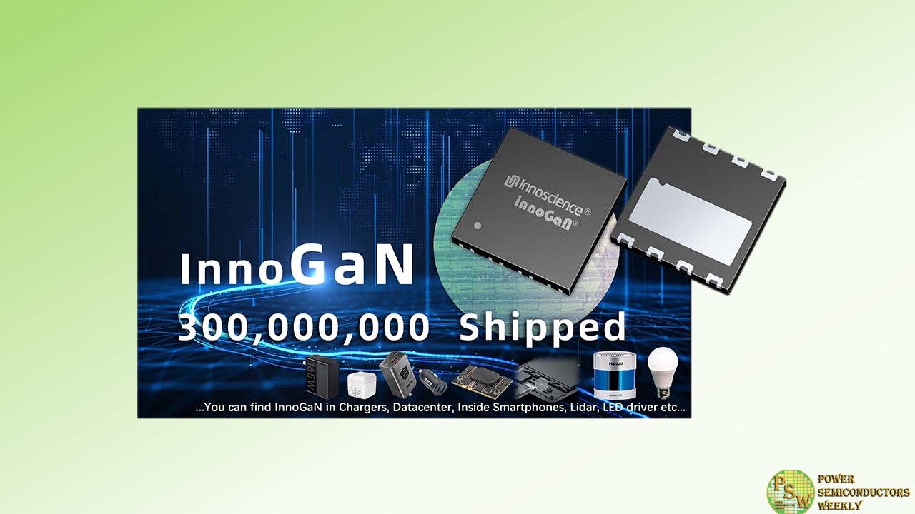
Innoscience Technology has shipped more than 300 million pieces of its InnoGan gallium nitride chips as of August 2023, helping customers achieve small size, high energy efficiency, and low loss product design.
This is in response to phenomenal market demand across multiple sectors multiple applications in the consumer category – fast charging, mobile phones, LEDs – as well as automotive LIDAR, data centres, and renewable energy and energy storage systems, which has seen analysts such as TrendForce’s in its 2023 GaN Power Semiconductor Market Analysis Report, state that “the global GaN power device market will grow from US$180 million in 2022 to US$1.33 billion in 2026, with compound growth rate of 65%”.
In November 2017, Innoscience began the world’s first 8-inch GaN-on-Si mass production line, adopting the Integrated Device Manufacturer (IDM) whole industry chain model, and launched its first low-voltage GaN power device in May 2018. By June 2019, Innoscience’s 650V high-voltage GaN device had passed JEDEC approval, and subsequently, Innoscience has been the only semiconductor company in the world that simultaneously mass-produces high-voltage and low-voltage GaN.
Market acceptance of Innoscience’s high quality, high performance GaN devices has been swift. Following its 2019 entry into the fast charging market, Innoscience’s 650V parts have been adopted in 30W-120W designs by leading brands including ASUS, Anker, Nubia, Baseus, Greenlink, and Flash.
In 2020, Innoscience’s 100V low-voltage GaN was successfully used by Hesai in mass-production LIDAR designs, allowing lasers to achieve image transmission in a shorter time.
In March 2021, the Tencent×Nubia Red Magic mobile phone 6Pro was released. It comes equipped as standard with industry’s first 120W Black Rubik’s Cube GaN fast charge, which is based on Innoscience’s 650V chip. With the successive adoption by Oppo, Vivo, Lenovo and other manufacturers, it has become an industry trend for mobile phones to be equipped with GaN fast charging as standard.
March 2021 saw the mass-production of Innoscience’s bi-directional conduction chip V-GaN officially begin; this device is the only GaN chip in the world that can be applied to high-voltage side load switches, smartphone USB/wireless charging ports with built-in OVP protection, multi-power supply system switch circuits, and other scenarios:one V-GaN replaces two Si MOSFETs in load switching applications resulting in a smaller and more efficient solution.
In October of the same year, Innoscience scored another industry first, as OPPO used the company’s self-developed bi-directional conduction VGaN IC as the internal power switch in its latest smart phone. Other mobile phone makers such as Realme, OnePlus, Lenovo, and Motorola have also successively adopted VGaN for charging protection.
In May 2022, Shounuo released the world’s smallest 45W/65W PD car charger, using Innoscience’s 40V low-voltage INN040FQ043A.
Then in July, Anker and Innoscience jointly released the world’s first 65W full-GaN fast charger. This design uses GaN power chips at both the AC and DC ends for the first time, taking system power density and efficiency to a whole new level.
Later, in October 2022, Innoscience achieved mass production of GaN products targeting industrial power supplies – again an industry first – comprehensively improving energy conversion efficiency and reducing system energy consumption.
In November 2022, Innoscience’s INN100W032A won the IIC World Electronics Achievement Award. The gate charge of this product is only 20% of a traditional silicon MOSFET, and its Ciss is only 40% of its silicon counterpart. It can be widely applied in motor drive, Class D, data centre, motor-driver, communication base station and other product fields. In January 2023, Innoscience launched the SolidGaN ISG3201, a 100V highly-integrated half-bridge drive packaged solution, further improving the overall system performance of 48V power supply of data centre module power supplies, motor drives, class D power amplifiers, photovoltaic inverters and light hybrid electric vehicles.
The move to GaN as the premium power semiconductor technology is driven both by new GaN products and market demands. As an example, in April this year, Innoscience’s IATF 16949 automotive-grade low-voltage parts successfully expanded from industrial to automotive applications, with use in autonomous vehicle LIDAR systems.
Then in July 2023, Innoscience began to apply GaN in the field of renewable energy, reducing the size and improving the efficiency of photovoltaic modules.
By the end of August 2023, Innoscience had successfully mass-produced 54 different types of high-voltage GaN chips (650V-700V) and 20 types of medium-low voltage GaN chips (30V-150V). Products span three chip categories: wafers, discrete devices and integrated solutions.
Commented Dr Denis Marcon, Innoscience’s General Manager, Europe: “We are just at the start of the GaN story. The first applications were all in consumer, but GaN is undoubtedly the key to reducing costs and increasing efficiency in the industrial field as well. And according to automotive industry forecasts, GaN may enter automotive market already this year penetrating applications such as low-power OBC and DC-DC applications in 2025.
With such rapid growth in market demand, the reliability of devices, price competitiveness and stable supply in large quantities are now the major concerns of users. Based on an advanced Innoscience’s 8-inch GaN-on-Si IDM manufacturing platform, Innoscience’s current production capacity has reached 15,000 wafers per month, providing tremendous advantages in scale, reliability and cost.”
Original – Innoscience Technology
-

IQE plc, the leading supplier of compound semiconductor wafer products and advanced material solutions to the global semiconductor industry, announced a strategic collaboration with VisIC Technologies, a global leader in the provision of GaN (Gallium Nitride) power solutions to the automotive sector, to develop the highest reliability gallium nitride D-Mode (D-Mode GaN) power products for use in electric vehicles inverters.
IQE and VisIC Technologies will collaborate to develop 200mm (8”) D-Mode GaN power epiwafers that will be developed at IQE’s UK facilities, leveraging IQE’s well-established expertise in GaN technology.
VisIC Technologies, with its ground-breaking D3GaN technology (Direct Drive D-Mode GaN), brings the future of EV inverters into focus. This technology promises to reduce power consumption, increase reliability and enhance performance in electric vehicles. By combining VisIC Technologies’ innovative Power Electronics solutions with IQE’s epitaxy excellence, this partnership aims to accelerate the adoption of GaN-on-Silicon technology in EVs, significantly contributing to the evolution of sustainable transportation.
The collaboration marks another important milestone in IQE’s strategy of diversification into the high-growth Power market, first announced at its 2022 Capital Markets Day. IQE sees significant opportunities in the GaN Power epiwafer market in particular, which is forecast to reach a $632m value by 2027.
Original – VisIC Technologies
-

Aehr Test Systems announced it has received an initial customer order for a FOX-NP™ wafer level test and burn-in system, multiple WaferPak™ Contactors, and a FOX WaferPak Aligner to be used for engineering, qualification, and small lot production wafer level test and burn-in of their silicon carbide devices. The customer is a US-based multibillion-dollar semiconductor supplier serving several markets including automotive, computing, consumer, energy, industrial, and medical. The FOX-NP system, including the FOX WaferPak Aligner and initial WaferPaks are scheduled per the customer’s requested accelerated schedule to ship by the end of the calendar year 2023.
The FOX-NP system is configured with the new Bipolar Voltage Channel Module (BVCM) and Very High Voltage Channel Module (VHVCM) options that enable new advanced test and burn-in capabilities for silicon carbide power semiconductors using Aehr’s proprietary WaferPak full wafer Contactors. This new order highlights Aehr’s continued progression within the growing silicon carbide global power market.
Gayn Erickson, President and CEO of Aehr Test Systems, commented, “We are very excited that after conducting a detailed financial evaluation and multiple onsite visits to Aehr’s application lab, this new customer selected our FOX-P solution for engineering, qualification, and production of their silicon carbide power devices.
This evaluation included cost of ownership and system throughput, as well as device test, burn-in, and stabilization coverage. As their production capacity increases, they told us that they will quickly move to our FOX-XP multi-wafer test and burn-in systems for high-volume production. In addition to the automotive electric vehicle device opportunity, this customer in particular sees the enormous opportunity for silicon carbide power devices in industrial, solar, and other power applications.
“William Blair forecasts that in addition to the 4.5 million six-inch equivalent wafers that will be needed to meet the demand for electric vehicle related silicon carbide devices in 2030, another 2.8 million wafers are needed to address industrial, solar, electric trains, energy conversion and other applications in 2030. The interesting part of this is that most of these applications will be served with discrete MOSFETS in single die packages.
The cost of ownership of our solution proved to be more cost-effective and efficient for these devices than package part burn-in after the die are packaged in packages such as TO-247 or other discrete packages. This is a strong testimony of the advantage of wafer level burn-in as a better alternative to package part burn-in. This expands our silicon carbide test and burn-in market even more and this new customer helps expand Aehr’s presence in this market as our total addressable market (TAM) continues to grow.
“Aehr’s FOX-P systems and proprietary WaferPak full wafer Contactors enable our customers to do economical production volume test and reliability burn-in with processes such as High Temperature Gate Bias (HTGB) and High Temperature Reverse Bias (HTRB) very cost-effectively and ensure extremely high device quality. Our systems are typically used for long burn-in times lasting up to 24 hours or more.
We can do this for under $5.00 per hour per wafer capital depreciation cost while testing and burning-in up to several thousand devices at a time per wafer. This is also in a test system footprint that is up to 94% less than a typical test system on a standard semiconductor wafer prober, which in a precious clean room wafer facility is extremely important and saves a great deal of cost.
“The FOX family of compatible systems including the FOX-NP and FOX-XP multi-wafer test and burn-in systems and Aehr’s proprietary WaferPak full wafer contactors provide a uniquely cost-effective solution for burning in multiple wafers of devices at a single time to remove early life failures of silicon carbide devices, which is critical to meeting the initial quality and long-term reliability of the automotive, industrial, and electrification infrastructure industry needs.”
The FOX-XP and FOX-NP systems, available with multiple WaferPak Contactors (full wafer test) or multiple DiePakTM Carriers (singulated die/module test) configurations, are capable of functional test and burn-in/cycling of devices such as silicon carbide and gallium nitride power semiconductors, silicon photonics as well as other optical devices, 2D and 3D sensors, flash memories, magnetic sensors, microcontrollers, and other leading-edge ICs in either wafer form factor, before they are assembled into single or multi-die stacked packages, or in singulated die or module form factor.
Original – Aehr Test Systems
-
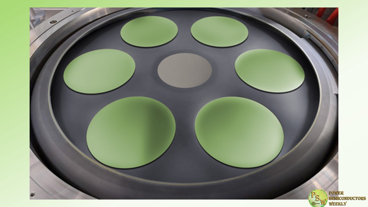
AIXTRON SE supports GlobiTech Inc., one of the world’s largest silicon-epitaxy foundries, to expand their business into silicon carbide (SiC) epitaxy. AIXTRON’s new G10-SiC has enabled this global leader to quickly ramp its SiC epitaxy production into high volume to address the world’s increasing demand for power epi-wafers. GlobiTech’s selection of the G10-SiC means a future-proof investment based on dual wafer size configuration of 9×150 & 6×200 mm and the highest throughput per fab space available in the SiC industry today.
The G10-SiC was officially introduced in September 2022. And it has quickly become the tool of record for both 150mm and 200mm SiC device makers as well as foundries like GlobiTech, the wholly owned subsidiary of GlobalWafers Co., Ltd., which manufactures silicon carbide and silicon epitaxial wafers focused on power and electric vehicle (EV) market segments.
“When one of the largest manufacturers and foundries like GlobiTech diversifies its business, it is a clear signal of a long-lasting trend in the semiconductor industry: conventional silicon is being replaced by silicon carbide in an ever-increasing number of applications. And it makes us proud when a leading company such as GlobiTech chooses AIXTRON and our new G10-SiC as an enabler of its transition intothis emerging SiC market. It confirms our overall strategy and the prospects for further growth”, says Dr. Felix Grawert, CEO and President of AIXTRON SE.
GlobiTech, located in Sherman, TX, is already in high-volume production using both G5WW C and G10-SiC AIXTRON systems, with continued installation capacity over the next years.Modeled after the silicon business, GlobiTech supplies both SiC substrates and SiC epitaxy to the market.
“In AIXTRON, we have found a strong partner supporting us in our vision and plans to expand our business into the SiC epitaxy market – an important step as SiC technology is one of the fastest-growing semiconductor sectors. AIXTRON tools allow us to get the most wafers out of our current fab. And AIXTRON’s team understands what it takes to compete against silicon to grow this market while offering great customer support and service”, says Mark England, President of GlobalWafers.
The G10-SiC is the first SiC epitaxy tool on the market that truly enables high-volume production of SiC epi-wafers. Since the G10-SiC offers both 9×150 mm and 6×200 mm batch configurations, it is an instrumental tool for a market rapidly transitioning from 6-inch (150mm) to 8-inch (200 mm) wafer diameters. The new platform is built around AIXTRON’s proven automated wafer cassette-to-cassette loading solution with high-temperature wafer transfer.
Combined with high growth rate process capabilities, the G10-SiC provides best-in-class wafer throughput, an excellent epi wafer performance in terms of quality and uniformity, and the best throughput per square meter of fab space. All this leads to the lowest cost of ownership in the market. It is estimated that in 2023, the new G10-SiC will become AIXTRON’s top-selling product.
The wide-bandgap material SiC is set to become mainstream technology for efficient power electronics. Driven by the growing adoption of SiC-based power semiconductors within e-mobility solutions and the overall acceleration of the charging infrastructure, the global demand for SiC wafers is growing rapidly.And with its superior characteristics, SiC semiconductors offer higher energy efficiency than conventional power electronics based on silicon. Therefore, SiC significantly contributes to reducing the global CO2 footprint.
Original – AIXTRON
