-
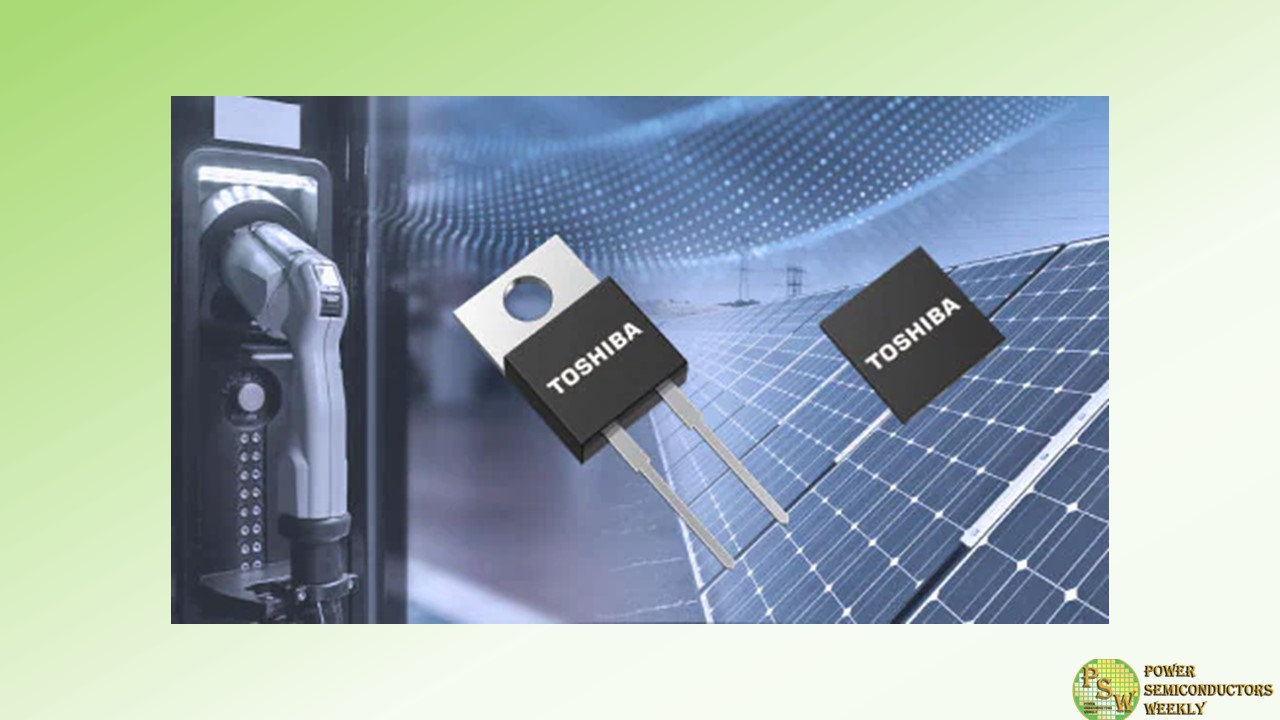
Toshiba Electronic Devices & Storage Corporation has launched the “TRSxxx65H series,” the company’s third and latest generation of silicon carbide (SiC) Schottky barrier diodes (SBDs) for industrial equipment. Volume shipments of the first 12 products, all 650V, start today, with seven products housed in TO-220-2L packages and five in DFN8×8 packages.
The new products use a new metal in a third generation SiC SBD chip that optimizes the junction barrier Schottky (JBS) structure of the second generation products. They achieve industry-leading low forward voltage of 1.2V (Typ.), 17% lower than the 1.45V (Typ.) of the previous generation.
They also improve the trade-offs between forward voltage and total capacitive charge, and between forward voltage and reverse current, which reduces power dissipation and contributes to high efficiency of equipment.
Applications
- Switching power supplies
- EV charging stations
- Photovoltaic inverters
Features
- Industry-leading low forward voltage: VF=1.2V (Typ.) (IF=IF(DC))
- Low reverse current:
TRS6E65H IR=1.1μA (Typ.) (VR=650V) - Low total capacitive charge:
TRS6E65H QC=17nC (Typ.) (VR=400V, f=1MHz)
Original – Toshiba
-
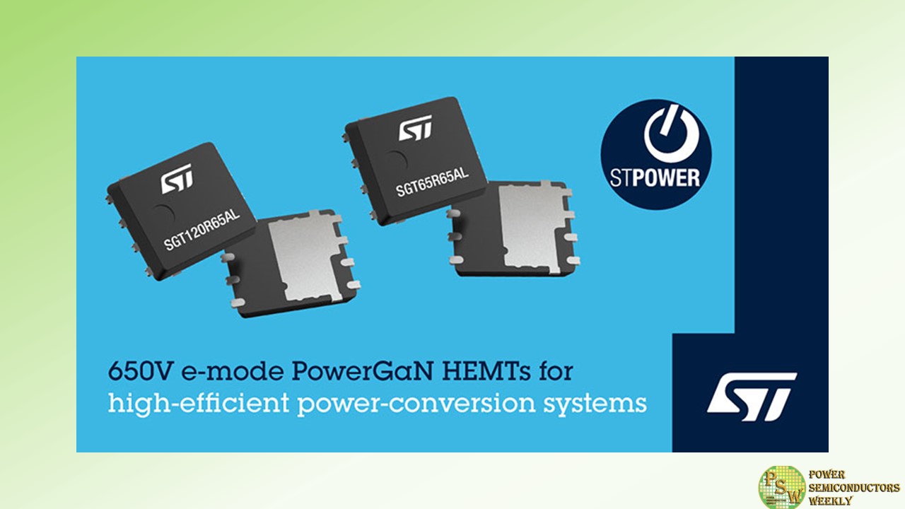
STMicroelectronics has begun volume production of e-mode PowerGaN HEMT (high-electron-mobility transistor) devices that simplify the design of high-efficiency power-conversion systems. The STPOWER™ GaN transistors raise performance in applications such as wall adapters, chargers, lighting systems, industrial power supplies, renewable energy applications, and in automotive electrification.
The first two products in the family, the SGT120R65AL and SGT65R65AL, are industrial-qualified 650V normally-off G-HEMT™ in a PowerFLAT 5×6 HV surface-mount package. They have current ratings of 15A and 25A, respectively, with typical on-resistance (RDS(on)) of 75mΩ and 49mΩ at 25°C.
Also, 3nC and 5.4nC total gate charge and low parasitic capacitances ensure minimal turn-on/turn-off energy losses. A Kelvin source connection allows optimized gate driving. In addition to the reduced size and weight of the power supplies and adapters, the two new GaN transistors provide higher efficiency, lower operating temperature, and extended life time.
In the coming months, ST will introduce new PowerGaN variants, i.e. automotive-qualified devices, as well as additional power-package options including PowerFLAT 8×8 DSC and LFPAK 12×12 for high power applications.
ST’s G-HEMT devices facilitate the transition to GaN wide-bandgap technology in power conversion. GaN transistors with the same breakdown voltage and RDS(on) as silicon alternatives can achieve lower total gate charge and parasitic capacitances, with zero reverse-recovery charge.
These properties raise efficiency and enhance switching performance, allowing higher switching frequency that permits smaller passive components thereby increasing power density. Applications can therefore become smaller with higher performance. In the future, GaN is also expected to enable new power-conversion topologies that will further improve efficiency and decrease power losses.
Original – STMicroelectronics
-

ROHM has reached a basic agreement with Solar Frontier K.K. to acquire the assets of Solar Frontier’s former Kunitomi Plant, located in Japan. The acquisition is scheduled to take place in October 2023 and will belong to the ROHM Group’s main production bases.
The role of semiconductors, one of ROHM’s core business fields is becoming increasingly important to achieving a decarbonized society.
In particular, the automotive and industrial equipment markets are undergoing technological innovation such as electrification in order to reduce environmental impact and achieve carbon neutrality. With this, the demand is increasing – especially for power and analog semiconductors.
As further expansion of the semiconductor market is expected, the ROHM Group intends to expand its production capacity continuously, particularly for silicon carbide (SiC) power devices, and ensure a stable supply to ROHM’s customers.
Original – ROHM
-
AdvanSiC has officially launched their project website. The objective of AdvanSiC is to develop, produce, test, and validate cost-effective HV SiC MOSFET semiconductors in MVDC grid applications, a full-scale wind converter, a full-scale solar inverter, and a solid-state circuit breaker for DC converter stations.
The aim is to minimize HV SiC device cost by advancing novel design structures and process optimization. Beyond this, we shall assure an immune and reliable environment to handle SiC fast transients, as well as optimize passives and cooling system to provide cost reduction not only at device level but also at system level.
The goal of AdvanSiC is to provide industrial leadership in key and emerging technologies to SMEs, start-ups, and industry from Europe to Europe, specifically in a technology that will be key to provide clean and affordable energy.
Original – AdvanSiC
-
Transphorm, Inc. responded to the recent news regarding China export restrictions. Late Monday, July 3, 2023, China’s Ministry of Commerce stated that it will restrict the exports of materials related to two metals used in semiconductor manufacturing: gallium and germanium. Gallium nitride (GaN) wafer materials are listed as being affected by these regulations.
Transphorm manufactures high voltage GaN power semiconductors. Trimethylgallium (TMGa) is used to produce the GaN. The company confirmed that its primary TMGa suppliers are not based in China and that suppliers have confirmed to be well-positioned to meet forecasted demand. Transphorm is therefore securely positioned to continue manufacturing and supplying its GaN devices without interruption.
Transphorm also explained gallium is generally a byproduct resulting from refinement processes used to produce popular metals such as aluminum from bauxite ore. Aluminum is produced in numerous countries such as Australia, Brazil, India, Jamaica, and the United States among others.
Transphorm will continue to the monitor the situation as necessary but sees no direct impact on its current operations. Nor does the company see long-term sourcing issues.
Original – Transphorm
-
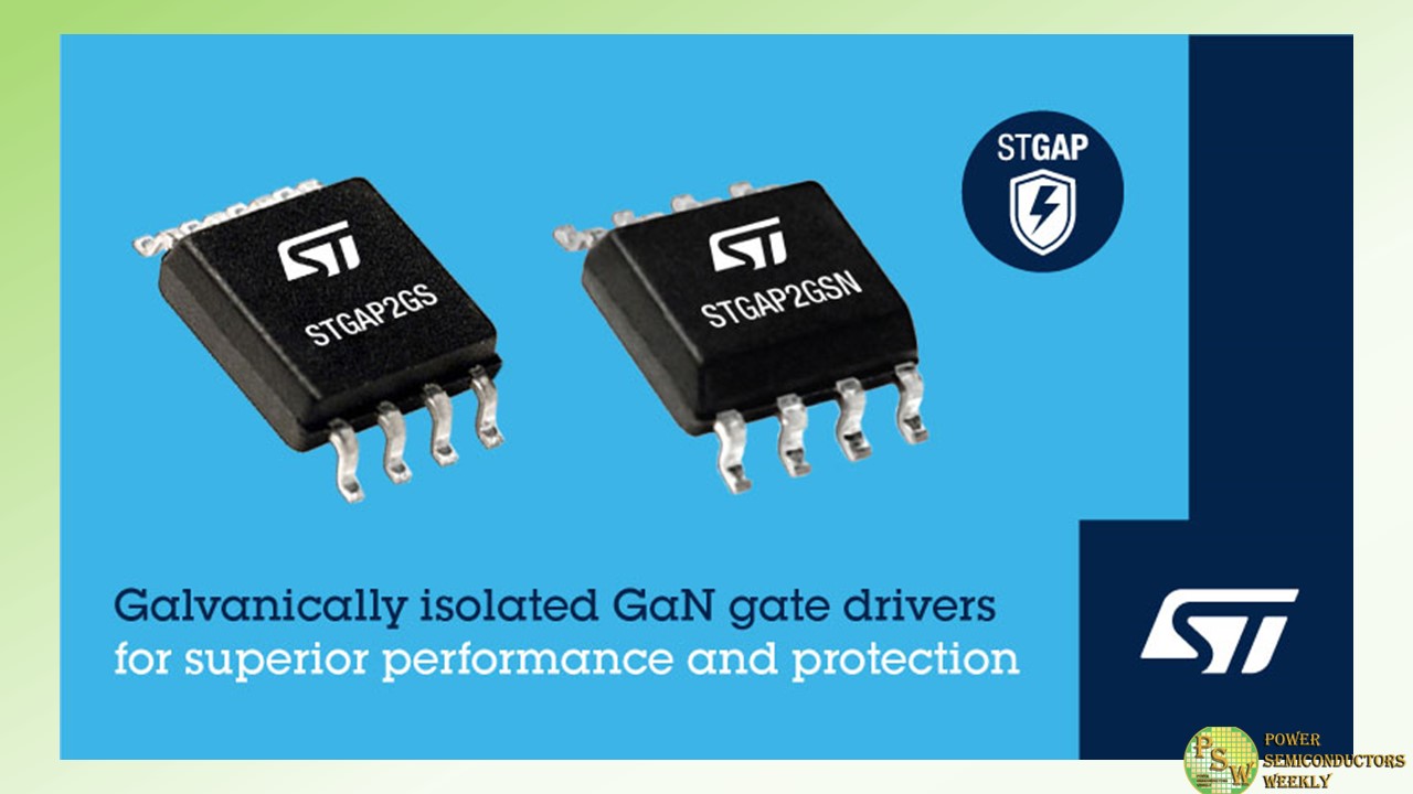
STMicroelectronics’ first galvanically isolated gate driver for gallium-nitride (GaN) transistors, the STGAP2GS, trims dimensions and bill-of-materials costs in applications that demand superior wide-bandgap efficiency with robust safety and electrical protection.
The single-channel driver can be connected to a high-voltage rail up to 1200V, or 1700V with the STGAP2GSN narrow-body version, and provides gate-driving voltage up to 15V. Capable of sinking and sourcing up to 3A gate current to the connected GaN transistor, the driver ensures tightly controlled switching transitions up to high operating frequencies.
With minimal propagation delay across the isolation barrier, at just 45ns, the STGAP2GS ensures fast dynamic response. In addition, dV/dt transient immunity of ±100V/ns over the full temperature range guards against unwanted transistor gate change. The STGAP2GS is available with separate sink and source pins for easy tuning of the gate-driving operation and performance.
Saving the need for discrete components to provide optical isolation, the STGAP2GS driver eases the adoption of efficient and robust GaN technology in various consumer and industrial applications. These include power supplies in computer servers, factory-automation equipment, motor drivers, solar and wind power systems, home appliances, domestic fans, and wireless chargers.
In addition to integrating galvanic isolation, the driver also features built-in system protection including thermal shutdown and under-voltage lockout (UVLO) optimized for GaN technology, to ensure reliability and ruggedness.
Two demonstration boards, the EVSTGAP2GS and EVSTGAP2GSN, combine the standard STGAP2GS and narrow STGAP2GSN with ST’s SGT120R65AL 75mΩ, 650V enhancement-Mode GaN transistors to help users evaluate the drivers’ capabilities.
The STGAP2GS in SO-8 widebody package, and the STGAP2GSN SO-8 narrow version, are available now, priced from $1.42 for orders of 1000 pieces.
Please visit www.st.com/stgap2gs for more information.
Original – STMicroelectronics
-

Navitas Semiconductor has confirmed continued supply of leading-edge gallium nitride (GaN) power ICs. On July 3rd, 2023, China’s Ministry of Commerce announced it would put in place certain restrictions on the exporting of gallium and germanium, among other materials, starting in August. Navitas’ wafer technology is ‘GaN-on-Si’. The wafer subcontract manufacturer has verified that their production remains unaffected by the export restrictions, given multiple sources of gallium world-wide.
As a result, Navitas does not expect customer deliveries to be impacted or its business to be adversely affected by the export restrictions.
Significant sources of gallium are available worldwide, as it is a natural by-product in the production of other metals such as aluminum. Navitas does not use germanium in any product.
Original – Navitas Semiconductor
-
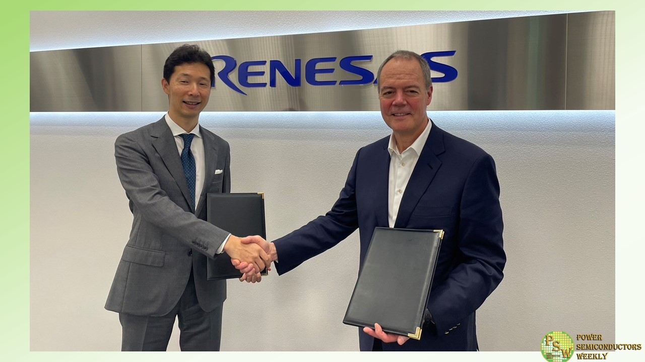
Renesas Electronics Corporation and Wolfspeed, Inc. announced the execution of a wafer supply agreement and $2 billion (USD) deposit by Renesas to secure a 10 year supply commitment of silicon carbide bare and epitaxial wafers from Wolfspeed. The supply of high-quality silicon carbide wafers from Wolfspeed will pave the way for Renesas to scale production of silicon carbide power semiconductors starting in 2025. The signing ceremony of the agreement was held at Renesas’ headquarters in Tokyo between Hidetoshi Shibata, President and CEO of Renesas, and Gregg Lowe, President and CEO of Wolfspeed.
The decade-long supply agreement calls for Wolfspeed to provide Renesas with 150mm silicon carbide bare and epitaxial wafers scaling in CY2025, reinforcing the companies’ vision for an industry-wide transition from silicon to silicon carbide semiconductor power devices. The agreement also anticipates supplying Renesas with 200mm silicon carbide bare and epitaxial wafers after the recently announced John Palmour Manufacturing Center for Silicon Carbide (the “JP”) is fully operational.
The need for more efficient power semiconductors, which supply and manage electricity, is dramatically increasing throughout automotive and industrial applications, spurred by the growth of electric vehicles (EVs) and renewable energy. Renesas is moving quickly to address the growing demand for power semiconductors by expanding its in-house manufacturing capacity. The company recently announced the restart of its Kofu Factory to produce IGBTs, and establishment of a silicon carbide production line at its Takasaki Factory.
Compared to conventional silicon power semiconductors, silicon carbide devices enable higher energy efficiency, greater power density and a lower system cost. In an increasingly energy-conscious world, the adoption of silicon carbide is becoming ever more pervasive across multiple high-volume applications spanning EVs, renewable energy and storage, charging infrastructure, industrial power supplies, traction and variable speed drives.
“The wafer supply agreement with Wolfspeed will provide Renesas with a stable, long-term supply base of high-quality silicon carbide wafers. This empowers Renesas to scale our power semiconductor offerings to better serve customers’ vast array of applications,” said Hidetoshi Shibata, President and CEO of Renesas. “We are now poised to elevate ourselves as a key player in the accelerating silicon carbide market.”
“With the steepening demand for silicon carbide across the automotive, industrial and energy sectors, it’s critically important we have best-in-class power semiconductor customers like Renesas to help lead the global transition from silicon to silicon carbide,” said Gregg Lowe, President and CEO of Wolfspeed. “For more than 35 years, Wolfspeed has focused on producing silicon carbide wafers and high-quality power devices, and this relationship marks an important step in our mission to save the world energy.”
The Renesas $2 billion deposit will help support Wolfspeed’s ongoing capacity construction projects including the JP, the world’s largest silicon carbide materials factory in Chatham County, North Carolina. The state-of-the-art, multi-billion-dollar facility is targeted to generate a more than 10-fold increase from Wolfspeed’s current silicon carbide production capacity on its Durham, North Carolina campus. The facility will produce primarily 200mm silicon carbide wafers, which are 1.7x larger than 150mm wafers, translating into more chips per wafer and ultimately, lower device costs.
Original – Renesas Electronics
-
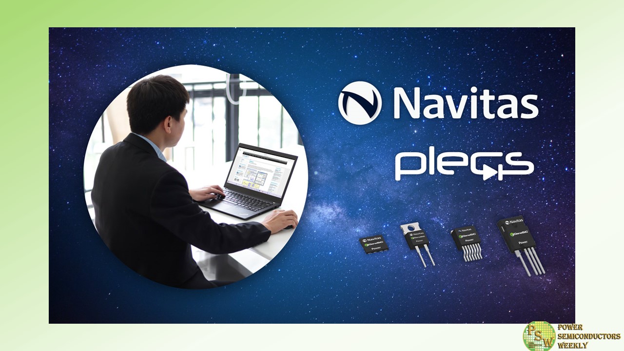
Navitas Semiconductor and Plexim GmbH announced a partnership to release GeneSiC G3™ SiC MOSFET and Gen 5 MPS diode PLECS thermal loss models for highly-accurate simulations of complete power electronics systems.
Power designers can simulate power and thermal losses in various soft- and hard-switching applications. Proprietary GeneSiC trench-assisted planar-gate MOSFET technology delivers the lowest RDS(ON) at high temperature and the highest efficiency at high speeds, and new MPS diodes with ‘low-knee’ characteristics drive unprecedented, industry-leading levels of performance, robustness and quality.
“Accurate, empirically-based simulation models maximize the chance of first-time-accurate designs, accelerating time-to-market and time-to-revenue,” noted Dr. Ranbir Singh, Navitas EVP for the GeneSiC business line. “For the power designer, understanding the leading-edge performance of GeneSiC MOSFETs and MPS diodes with detailed device characteristics, plus power, efficiency and thermal analysis is a critical competitive advantage.”
“The intuitive and highly-efficient PLECS lookup-table based approach to simulating thermal semiconductor losses in complex power electronic circuits is key,” said Kristofer Eberle, Plexim, North America. “Unlike legacy modeling approaches that are not well-suited to new wide bandgap materials, PLECS uses a simplified, but accurate behavioral description to highlight the superior performance of the GeneSiC MOSFETs.”
PLECS models for GeneSiC MOSFETs and MPS diodes are available via genesicsemi.com.
Original – Navitas Semiconductor
-

Kulicke and Soffa Industries, Inc. announced the launch of several new systems and capabilities serving high-volume semiconductor and fast-growing power-semiconductor applications.
POWERCOMM™ and POWERNEXX™ represent the next evolution in advanced wire bonding systems and are designed with a new generation of intuitive advanced process capabilities which deliver maximum levels of performance, efficiency, and productivity. Additionally, both systems deliver enhanced mean time between assists (MTBA), with automated recovery features that improve the machine to operator ratio and better support localization of semiconductor assembly.
The POWERCOMM™ advanced wire bonding solution is designed to support high-volume discrete and low-pin count devices commonly used in applications such as data centers, automotive, industrial automation, smartphones, wearables and connected devices.
The POWERNEXX™ advanced wire bonding solution is optimized for higher density QFN packages with widths of up to 100mm. The improved illumination design on POWERNEXX™ allows faster alignment time through its Pattern Recognition System (PRS). Faster alignment and advanced process capabilities deliver the industry leading UPH and lowest Cost-of-Ownership.
In addition to the new POWERCOMM™ and POWERNEXX™ systems, K&S extends its leadership in wedge bond applications with new High-Power-Interconnect (HPI) capabilities addressing the emerging needs of power devices. HPI capabilities are becoming increasingly necessary to assemble applications such as inverters, battery assembly and charging infrastructure which support the growth and increasing efficiency requirements of sustainable energy and electric vehicle applications. The need for more efficient and higher-current applications are driving rapid changes to the power semiconductor market by increasing demand in emerging compound semiconductors, such as Silicon Carbide (SiC) and Gallium Nitride (GaN), but are also demanding new capabilities to support next-generation battery assembly and are accelerating the transition from aluminum wire and ribbon, to copper wire and ribbon. Next generation HPI capabilities are being introduced across Kulicke & Soffa’s leading wedge bonder portfolio today.
“Our rich history of innovation and ongoing development priorities are enabling us to provide additional value to the increasingly critical assembly process. This recent set of new wire bonding systems and capabilities will better enable customers to optimize productivity, improve material handling capabilities and significantly lower cost-of-ownership,” said Shawn Sarbacker, Kulicke and Soffa’s Vice President of Ball Bonder Business Unit.
Original – Kulicke and Soffa Industries
