-

DENSO Corporation and Fuji Electric Co., Ltd. announced that a semiconductor supply plan submitted jointly by the companies has been approved by the Ministry of Economy, Trade and Industry. Under this plan, the companies will take part in joint investment and production of silicon carbide (SiC) power semiconductors to develop and strengthen frameworks for the supply of said semiconductors.
Power semiconductors are vital to the efficient supply of electric power. Demand for power semiconductors has been rising rapidly given that they are used in electrified vehicles, which are being adopted at an accelerated pace amid the push for the decarbonization of society. In comparison to prior silicon semiconductors, SiC power semiconductors are able to deliver superior performance under high temperature, high-frequency, and high-voltage conditions.
These devices are therefore anticipated to make large contributions to reductions in power loses as well as to more compact and lighter-weight designs for battery electric vehicle systems and other power electronics. Accordingly, growth in demand is projected for SiC power semiconductors.
In response to electrification trends, DENSO has advanced SiC technology development projects targeting increased quality and efficiency in relation to everything from wafers and element devices to modules and inverters. Meanwhile, Fuji Electric has constructed extensive frameworks encompassing all tasks spanning from the development of SiC power semiconductor elements that enable increased efficiency and more compact designs for power electronics equipment to mass production of the related modules.
Based on the approved plan, these companies will combine their respective automotive product development and production technology capabilities in a joint effort to expand their capacity for the efficient and stable supply of SiC power semiconductors throughout Japan.
Through this partnership, the companies will contribute to the development of semiconductor supply frameworks within Japan and to the improvement of the international competitiveness of Japan’s domestic semiconductor and automotive industries. In addition, this partnership is anticipated to help advance the decarbonization of society.
Original – Fuji Electric
-

Valeo, a leading automotive technology company, and ROHM Semiconductor collaborate to propose and optimize the next generation of power modules for electric motor inverters using their combined expertise in power electronics management. As a first step, ROHM will provide its 2-in-1 Silicon Carbide (SiC) molded module TRCDRIVE pack™ to Valeo for future powertrain solutions.
Valeo is broadening access to efficient, electrified mobility across various vehicle types and markets from the smallest one (ebikes), through the mainstream (passenger cars) to the biggest one (eTrucks). By combining Valeo’s expertise in mechatronics, thermal management and software development with ROHM’s power modules, Valeo drives the power electronics solution forward, contributing to the performance, efficiency, and decarbonization of automotive systems worldwide.
Valeo and ROHM have been collaborating since 2022, initially focusing on technical exchanges aimed at improving the performance and efficiency of the motor inverter – a key component in the propulsion systems of electric vehicles (EVs) and plug-in hybrids (PHEVs). By refining power electronics, both companies aim to offer optimized cost/performance by delivering higher energy efficiency, reducing heat generation thanks to an optimized cooling and mechatronic integration, and increasing overall reliability with a SiC packaging.
“This partnership marks, for Valeo Power Division, a significant step forward in delivering advanced and high-efficient power electronics,” says Xavier DUPONT, Valeo Power Division CEO. “Together, we aim to set new industry standards for high voltage inverters and accelerate the transition towards more efficient and affordable electric mobility.”
“We are pleased to support Valeo, a renowned automotive supplier, with our power semiconductors. ROHM’s TRCDRIVE pack™ provides high power density, leading to an improved power efficiency. Together, we contribute to the development of highly efficient powertrains by fostering the collaboration with Valeo,” says Wolfram HARNACK, President ROHM Semiconductor GmbH.
These evolutions are all essential to supporting the growing demand for longer range, faster charging capabilities, and, overall a high-performance and an affordable inverter for BEVs and PHEVs.
Valeo will start supplying a first series project in early 2026. Valeo and ROHM will contribute to the improvement of efficiency and downsizing of Valeo’s next generation of xEV inverters.
Original – ROHM
-
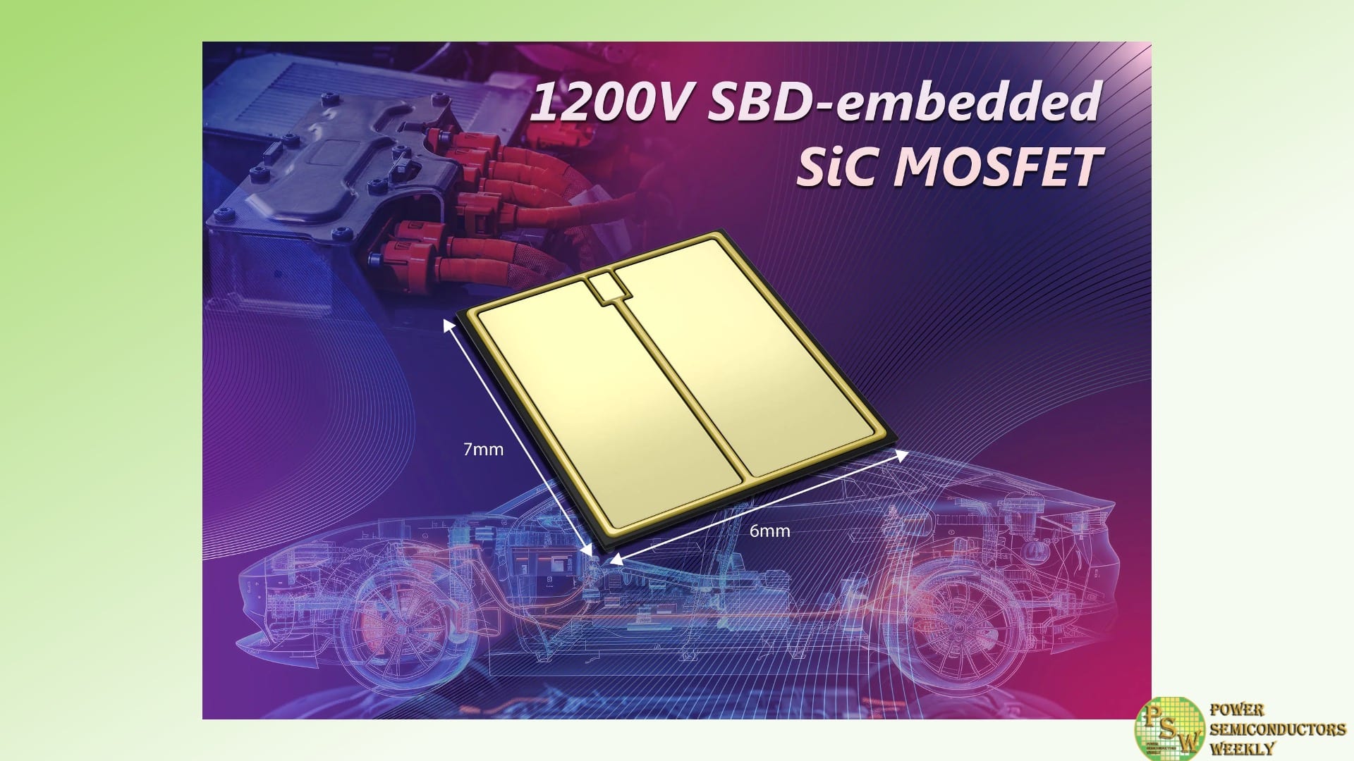
Toshiba Electronics Europe GmbH has developed new 1200V silicon carbide (SiC) MOSFETs with low on-resistance (RDS(ON)) and high levels of reliability. The devices are particularly suited to applications within automotive traction inverters. They are now available and shipping as early test samples in bare die format – allowing customers to customise them to meet the needs of their applications.
The new X5M007E120 uses a manufacturing process that reduces on-resistance per unit area by up to 30%. Unlike existing methods that utilise a striped-pattern construction, the new devices arrange the embedded Schottky barrier diodes (SBDs) in a check-pattern to achieve lower on-resistance.
Many SiC MOSFETs increase on-resistance as body diodes are energised during reverse conduction, which can lead to reliability issues. Toshiba SiC MOSFETs alleviate this issue by preventing body diodes from operating as SBDs are embedded into the MOSFETs. This approach maintains the reduction in on-resistance while ensuring reliability during reverse conduction.
With electric motors consuming over 40% of the world’s electrical energy, efficient operation is essential to sustainability. The re-arrangement of SBDs in this device has suppressed body diode energisation, and the upper limit of unipolar operation has increased to around double without increasing the SBD mounting area. Additionally, channel density is improved. These enhancements contribute to energy efficiency in applications, including motor control inverters.
Reducing RDS(ON) within a SiC MOSFET can cause excess current flow during short-circuit operations. By adopting a deep barrier structure, the X5M007E120 reduces excessive current within the MOSFET section and leakage current in the SBDs section during short-circuit operation. This enables durability during short-circuit conditions while maintaining high levels of reliability against reverse conduction operation.
The new X5M007E120 has a VDSS of 1200V and is rated for a drain current (ID) of 229A continuously, with 458A for pulsed operation (ID Pulse). RDS(ON) is as low as 7.2mΩ, and the device can operate with channel temperatures (Tch) as high as 175°C. The devices are AEC-Q100 qualified for automotive applications.
Engineering samples of the new X5M007E120 are expected to ship during 2025, with mass production samples scheduled to start in 2026.
Toshiba will continue to seek ways to further improve the characteristics of its products. The company will contribute to realising a decarbonised society by providing customers with power semiconductors for applications where energy efficiency is essential, such as inverters for motor control and power control systems for electrical vehicles.
Original – Toshiba
-
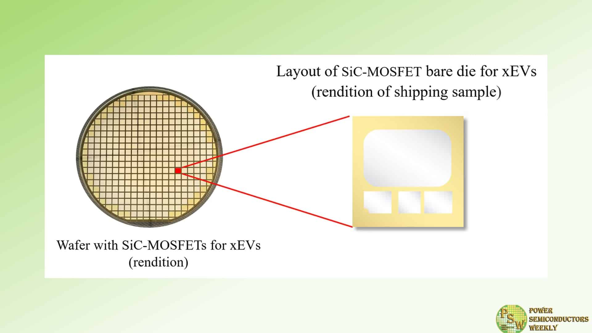
Mitsubishi Electric Corporation announced that it will begin shipping samples of a silicon carbide (SiC) metal-oxide-semiconductor field-effect transistor (MOSFET) bare die for use in drive-motor inverters of electric vehicles (EVs), plug-in hybrid vehicles (PHEVs) and other electric vehicles (xEVs) on November 14.
Mitsubishi Electric’s first standard-specification SiC-MOSFET power semiconductor chip will enable the company to respond to the diversification of inverters for xEVs and contribute to the growing popularity of these vehicles. The new SiC-MOSFET bare die for xEVs combines a proprietary chip structure and manufacturing technologies to contribute to decarbonization by enhancing inverter performance, extending driving range and improving energy efficiency in xEVs.
Mitsubishi Electric’s new power semiconductor chip is a proprietary trench SiC-MOSFET that reduces power loss by about 50% compared to conventional planar SiC-MOSFETs. Thanks to proprietary manufacturing technologies, such as a gate oxide film process that suppresses fluctuations in power loss and on-resistance, the new chip achieves long-term stability to contribute to inverter durability and xEV performance.
Original – Mitsubishi Electric
-

Cambridge GaN Devices (CGD) and IFP Energies nouvelles (IFPEN), a major French public research and training organization in the fields of energy, transport and the environment, have developed a demo which confirms the suitability of CGD’s ICeGaN®650 V GaN ICs in a multi-level, 800 VDC inverter.
The demo delivers super-high power density – 30 kW/l – which is greater than can be achieved by more expensive, state-of-the-art silicon-carbide (SiC)-based devices. The inverter realization also demonstrates the ease of paralleling that ICeGaN technology enables; each inverter node has three 25mΩ / 650V ICeGaN ICs – 36 devices in total – in parallel.
ANDREA BRICCONI | CHIEF MARKETING OFFICER, CGD
“We are super excited at this first result of our partnership with IFPEN. 800 VDC supports the 800 V bus which is being increasingly adopted by the EV industry. By addressing automotive and other high voltage inverter applications with energy-efficient ICeGaN-based solutions we are delivering on CGD’s key commitment – sustainability.”This multi-level GaN Inverters can power electric motors to over 100 kW peak, 75 kW continuous power. The CGD/IFPEN demo features: a high voltage input of up to 800Vdc; 3-phase output; a peak current of 125 Arms (10s) (180 Apk); and a continuous current of 85 Arms continuous (120 Apk).
The ICeGaN multi-level design proposed by IFPEN reveals several compelling benefits:
- Increased Efficiency: the improvement in the efficiency of the traction inverter leads to an increase in battery range and a reduction in charging cycles. It also leads to a reduction in battery cost if the initial range (iso-range) is maintained
- Higher switching frequencies: GaN transistors can operate at much higher frequencies than silicon transistors. This reduces iron losses in the motor, particularly in the case of machines with low inductances
- Reduced Electromagnetic Interferences: 3-level topology minimizes EMI and enhances the reliability of the system
- Enhanced thermal management: insulated metallized substrate boards featuring an aluminium core facilitate superior thermal dissipation, ensuring optimal operating temperatures and extending the lifespan of the system and associated GaN devices
- Modular design: this facilitates scalability and adaptability for varying system requirements.
GAETANO DE PAOLA | PROGRAM MANAGER, IFPEN
“Following the implementation of this inverter reference using CGD’s enabling ICeGaN ICs coupled with innovative topologies, such as multi-level solutions, IFPEN now strongly believes that GaN is a breakthrough technology in terms of performance and cost for high-voltage traction inverters.”Original – Cambridge GaN Devices
-

ROHM has developed surface mount SiC Schottky barrier diodes (SBDs) that improve insulation resistance by increasing the creepage distance between terminals. The initial lineup includes eight models – SCS2xxxNHR – for automotive applications such as onboard chargers (OBCs), with plans to deploy eight models – SCS2xxxN – for industrial equipment such as FA devices and PV inverters in December 2024.
The rapidly expanding xEV market is driving the demand for power semiconductors, among them SiC SBDs, that provide low heat generation along with high-speed switching and high-voltage capabilities in applications such as onboard chargers. Additionally, manufacturers increasingly rely on compact surface mount devices (SMDs) compatible with automated assembly equipment to boost manufacturing efficiency. Compact SMDs tend to typically feature smaller creepage distances, fact that makes high-voltage tracking prevention a critical design challenge.
As leading SiC supplier, ROHM has been working to develop high-performance SiC SBDs that offer breakdown voltages suitable for high-voltage applications with ease of mounting. Adopting an optimized package shape, it achieves a minimum creepage distance of 5.1mm, improving insulation performance when contrasted with standard products.
The new products utilize an original design that removes the center pin previously located at the bottom of the package, extending the creepage distance to a minimum of 5.1mm, approx. 1.3 times greater than standard products. This minimizes the possibility of tracking (creepage discharge) between terminals, eliminating the need for insulation treatment through resin potting when surface mounting the device on circuit boards in high voltage applications. Additionally, the devices can be mounted on the same land pattern as standard and conventional TO-263 package products, allowing an easy replacement on existing circuit boards.
Two voltage ratings are offered, 650V and 1200V, supporting 400V systems commonly used in xEVs as well as higher voltage systems expected to gain wider adoption in the future. The automotive-grade SCS2xxxNHR are AEC-Q101 qualified, ensuring they meet the high reliability standards this application sector demands.
Going forward, ROHM will continue to develop high-voltage SBDs using SiC, contributing to low energy consumption and high efficiency requirements in automotive and industrial equipment by providing optimal power devices that meet market needs.
Original – ROHM
-

Cambridge GaN Devices (CGD) and Qorvo® have partnered to bring together industry-leading motor control and power efficiency technologies in the PAC5556A + ICeGaN® evaluation kit (EVK). This collaboration combines Qorvo’s high-performance BLDC/PMSM motor controller/driver and CGD’s easy-to-use ICeGaN ICs in a board that significantly improves motor control applications.
ANDREA BRICCONI | CHIEF MARKETING OFFICER, CGD
“By combining industry-leading solutions from our two technology-strong companies in this EVK, we are enabling the development of compact, energy-efficient systems with high power density. Unlike other GaN implementations, ICeGaN technology easily interfaces with Qorvo’s PAC5556A motor control IC for seamless high performance in BLDC and PMSM applications.”JEFF STRANG | GENERAL MANAGER, POWER MANAGEMENT BUSINESS UNIT, QORVO
“Wide-bandgap semiconductors like GaN and SiC are being integrated into motor control applications for the power density and efficiency advantages they offer. CGD’s ICeGaN technology delivers ease of use and reliability – two critical factors for motor control and drive designers. Customers are responding enthusiastically when they experience the power of GaN combined with our highly integrated PAC5556A 600V BLDC motor control solution.”By employing CGD’s latest-generation P2 ICs, the PAC5556AEVK2 evaluation kit with 240 mΩ ICeGaN achieves up to 400W peak performance without a heatsink, whilst the PAC5556AEVK3 with 55 mΩ ICeGaN hits 800W peak with minimal airflow cooling.
ICeGaN’s efficiency gains result in reduced power loss, increased power availability, and minimized heat dissipation, enabling smaller and more reliable systems. Because ICeGaN integrates essential current sense and Miller clamp elements, gate driver design is simplified and BOM costs are reduced. This makes the solution easy to implement and price-competitive, as well as high performance.
The PAC5556A + CGD GaN EVKs offer higher torque at low speeds and precise control, making them ideal for white goods, ceiling fans, refrigerators, compressors and pumps. Target markets include industrial and home automation, especially where compact, high-efficiency motor control systems are required. PAC5556AEVK2 and PAC5556AEVK3 are now available to order at Qorvo’s website.
Original – Cambridge GaN Devices
-

Efficient Power Conversion (EPC) announced that the Full Commission of the U.S. International Trade Commission (ITC) has affirmed the ITC’s initial determination that Innoscience infringed EPC’s foundational patent for GaN technology, which is core to applications involving artificial intelligence, satellites, rapid chargers, humanoid robots, and autonomous driving, among others. The decision imposes a ban on Innoscience (Zhuhai) Technology Co., Ltd. and its affiliates (Innoscience) from importing GaN-related products into the United States without a license from EPC.
This milestone decision marks the first successfully litigated U.S. patent dispute involving GaN-based wide bandgap semiconductors and solidifies EPC’s position as a leading developer of these next-generation devices, which are significantly more efficient, faster, and smaller than traditional, silicon-based technology. The decision also paves the way for EPC to expand access to its IP through licensing agreements with potential partners and customers around the world.
“After pouring nearly two decades and immense resources into developing our uniquely valuable intellectual property portfolio, this is a tremendous victory for EPC and a major win for fair competition globally, which is critical to the success of next-generation technological advances. We are grateful to the ITC for their diligent work in recognizing the validity of our patents and Innoscience’s infringement,” said Alex Lidow, CEO and Co-Founder of EPC. “EPC will continue to vigorously defend our IP against unfair use to ensure that we can continue to innovate and provide our customers with the cutting-edge technologies needed to help power our future.”
The ITC’s most recent decision is the fourth time that EPC’s IP rights have been affirmed against Innoscience in the past six months. EPC initially filed the infringement claim against Innoscience in the ITC in May 2023. In response, Innoscience challenged the validity of the EPC patents at issue in the U.S., as well as EPC’s counterpart patents in China.
The China National Intellectual Property Administration upheld the validity of EPC’s counterpart patents in April and May 2024. The ITC’s initial determination in July 2024 similarly confirmed the validity of the challenged patents, and also found that Innoscience infringed EPC’s foundational patent, U.S. Patent No. 8,350,294. The ITC’s final determination is subject to a 60-day Presidential review period, expiring on January 6, 2025.
Original – Efficient Power Conversion
-

Stellantis N.V. and Infineon Technologies AG will work jointly on the power architecture for Stellantis’ electric vehicles to support Stellantis’ ambition of offering clean, safe and affordable mobility to all.
To support this, the companies have signed major supply and capacity agreements that will serve as the foundation for the planned collaboration to develop the next generation of power architecture, including:
- Infineon’s PROFET™ smart power switches, which will replace traditional fuses, reduce wiring and enable Stellantis to become one of the first automakers to implement intelligent power network management.
- Silicon carbide (SiC) semiconductors, which will support Stellantis in its efforts to standardize its power modules, improve the performance and efficiency of EVs while also reducing costs.
- AURIX TM microcontrollers, which target the first generation of the STLA Brain zonal architecture.
Stellantis and Infineon are also in the process of extending their cooperation with the implementation of a Joint Power Lab to define the next-generation scalable and intelligent power architecture enabling Stellantis’ software-defined vehicle.
“As outlined in our strategic plan, Dare Forward 2030, we are securing the supply of crucial semiconductor solutions required to continue our transition to an electrified future leveraging innovative E/E architectures for our next-generation platforms,” said Maxime Picat, Stellantis Chief Purchasing and Supplier Quality Officer.
“Infineon is now entering a collaboration and innovation partnership with Stellantis,” said Peter Schiefer, President of Infineon’s Automotive Division. “As the world’s leading automotive semiconductor vendor, we bring our product-to-system expertise and dependable electronics to the table. Our semiconductors drive the decarbonization and digitalization of mobility. They increase the efficiency of cars and enable software-defined architectures that will significantly improve the user experience.”
With the world`s most cost-competitive SiC fab in Kulim, Malaysia, the upcoming 300-millimeter ”Smart Power Fab” in Dresden, Germany, and the joint venture with TSMC and partners (ESMC) as well as accompanying supply agreements with foundry partners, Infineon is ready to fully meet market demand for automotive semiconductor solutions. According to the market research company TechInsights, Infineon is the global number one supplier of automotive microcontrollers with a market share of about 29 percent of the global automotive microcontroller market.
Original – Infineon Technologies
-
 LATEST NEWS / PRODUCT & TECHNOLOGY / SiC / WBG
STMicroelectronics Released an Advanced Galvanically Isolated Gate Drivers for IGBTs and SiC MOSFETs
November 7, 2024
2 Min ReadSTMicroelectronics’ STGAP3S family of gate drivers for silicon-carbide (SiC) and IGBT power switches combines ST’s latest robust galvanic isolation technology with optimized desaturation protection and flexible Miller-clamp architecture.
Featuring reinforced capacitive galvanic isolation between the gate-driving channel and the low-voltage control and interface circuitry, the STGAP3S withstands 9.6kV transient isolation voltage (VIOTM) with 200V/ns common-mode transient immunity (CMTI). With its state-of-the-art isolation, the STGAP3S enhances reliability in motor drives for industrial applications such as air conditioning, factory automation, and home appliances. The new drivers are also used in power and energy applications including charging stations, energy storage systems, power-factor correction (PFC), DC/DC converters, and solar inverters.
The STGAP3S product family includes different options with 10A and 6A current capability, each of them available with differentiated Under Voltage Lock-Out (UVLO) and desaturation intervention thresholds. This helps designers select the best device to match the performance of their chosen SiC MOSFET or IGBT power switches.
The Desaturation protection implements an overload and short-circuit protection for the external power switch providing the possibility to adjust the turn-off strategy using an external resistor to maximize the protection turn-off speed while avoiding excessive overvoltage spikes. The undervoltage-lockout protection prevents turn-on with insufficient drive voltage.
The driver’s integrated Miller Clamp architecture provides a pre-driver for an external N-channel MOSFET. Designers can thus leverage flexibility to select a suitable intervention speed that prevents induced turn-on and avoids cross conduction.
The available device variants allow a choice of 10A sink/source and 6A sink/source drive-current capability for optimum performance with the chosen power switch with desaturation-detection and UVLO thresholds optimized for IGBT or SiC technology. The fault conditions of desaturation, UVLO and overtemperature protection are notified with two dedicated open drain diagnostic pins.
Original – STMicroelectronics
