-

Navitas Semiconductor has announced the world’s first 8.5 kW power supply unit (PSU), powered by GaN and SiC technologies to achieve 98% efficiency, for next-generation AI and hyperscale data centers.
The AI-optimized 54V output PSU complies with Open Compute Project (OCP) and Open Rack v3 (ORv3) specifications and utilizes high-power GaNSafe and Gen-3 Fast SiC MOSFETs configured in 3-phase interleaved PFC and LLC topologies, to ensure the highest efficiency and performance, with lowest component count. The PSU’s shift to a 3-phase topology for both the PFC and LLC (vs. 2-phase topologies used by competing PSUs) enables the industry’s lowest ripple current and EMI.
Furthermore, the PSU reduces the number of GaN and SiC devices by 25% compared with the nearest competing system, which reduces the overall cost. The PSU has an input voltage range of 180 to 264 Vac, a standby output voltage of 12 V, and an operating temperature range of -5oC to 45oC. Its hold-up time at 8.5 kW is 10 ms, with 20 ms possible through an extender.
The 3-Phase LLC topology is enabled by high-power GaNSafe, which is specifically created for demanding, high-power applications, such as AI data centers and industrial markets. Navitas’ 4th generation integrates control, drive, sensing, and critical protection features that enable unprecedented reliability and robustness. GaNSafe is the world’s safest GaN with short-circuit protection (350ns max latency), 2kV ESD protection on all pins, elimination of negative gate drive, and programmable slew rate control. All these features are controlled with 4-pins, allowing the package to be treated like a discrete GaN FET, requiring no VCC pin. Suitable for applications from 1 kW to 22 kW, 650 V GaNSafe in TOLL and TOLT packages are available with a range of RDS(ON)MAX from 25 to 98 mΩ.
The 3-Phase interleaved CCM TP-PFC is powered by Gen-3 Fast SiC MOSFETs with ‘trench-assisted planar’ technology, which has been enabled by over 20 years of SiC innovation leadership and offers world-leading performance over temperature, delivering cool-running, fast-switching, and superior robustness to support faster charging EVs and up to 3x more powerful AI data centers.
“This complete wide bandgap solution of GaN and SiC enables the continuation of Navitas’ AI power roadmap which enables this 8.5kW and plans to drive to 12kW & higher in the near-term”, said Gene Sheridan, CEO and co-founder of Navitas. “As many as 95% of the world’s data centers cannot support the power demands of servers running NVIDIA’s latest Blackwell GPUs, highlighting a readiness gap in the ecosystem. This PSU design directly addresses these challenges for AI and hyperscale data centers.”
The PSU will be on display for the first time at Electronica 2024 (Hall C 3, booth 129, November 12th– 15th).
Original – Navitas Semiconductor
-

SemiQ will exhibit its latest SiC power solutions for high-voltage applications at electronica 2024, the world’s leading electronics trade fair and conference, in Munich from November 12-15.
Visitors to SemiQ will be able to explore the company’s latest advancements in high-voltage technology. This includes the debut of the next generation of 1200V SiC MOSFETs and SemiQ’s QSiC portfolio of ultra-efficient modules, supporting innovations in EVs, renewable energy, motor drives, medical power supplies and high-power solar applications.
Engineered with high-performance ceramics, QSiC™ MOSFET modules offer industry-leading reliability in a compact form factor and have been designed to specifically meet the stringent demands for high-power, high-frequency applications. Each module undergoes wafer-level gate burn-in testing to ensure high-quality gate oxide and stable gate threshold voltage.
Dr. Timothy Han, President of SemiQ said: “Our solutions significantly enhance the performance and efficiencies necessary to propel the industry forward, unlocking yet more high-power applications. We look forward to demonstrating how these innovative technologies will pave the way for fresh designs and advancements in the industry.”
Electronica will take place at the Messe München in Munich, Germany, from November 12-15, 2024. SemiQ’s stand is at Alfatec’s booth in Hall A5, Booth 421.
Original – SemiQ
-
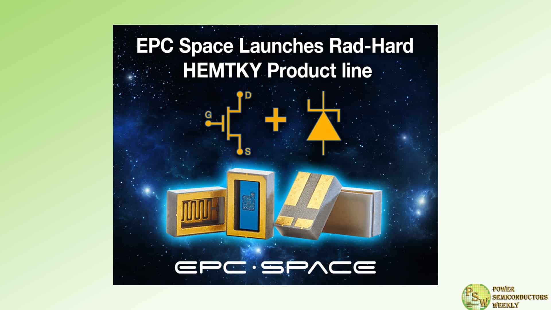
EPC Space announced the launch of HEMTKY product line.
A HEMTKY is a HEMT, High Electron Mobility Transistor, with an embedded Schottky diode. The presence of an antiparallel Schottky diode in the HEMTKY structure minimizes third quadrant conduction losses absent GaN HEMT synchronous drive. Notable advantages are:
- Predictable conduction losses, no reverse recovery charge
- Reduced system sensitivity to half-bridge deadtime variance
- Reduced negative voltage stress on gate drivers
For 500-unit quantities, engineering models are priced at $212 USD each, while space level units are priced at $315 USD each.
EPC Space provides revolutionary high-reliability radiation-hardened enhancement-mode gallium nitride power management solutions for space and other harsh environments. Radiation hardened GaN-based power devices address critical spaceborne environments for applications such as power supplies, motor drives, ion thrusters, and more. eGaN is a registered trademark of Efficient Power Conversion Corporation, Inc.
Original – EPC Space
-

Nexperia announced that it has entered into a strategic partnership with KOSTAL, a leading automotive supplier, which will enable it to produce wide bandgap (WBG) devices that more closely match the exacting requirements of automotive applications. Under the terms of this partnership, Nexperia will supply, develop, and manufacture WBG power electronics devices which will be designed-in and validated by Kostal. The collaboration will initially focus on the development of SiC MOSFETs in topside cooled (TSC) QDPAK packaging for onboard chargers (OBC) in electric vehicles (EV).
KOSTAL Automobil Elektrik, with over a century of experience, is a key player in the global automotive industry. Nearly one in every two cars worldwide is equipped with KOSTAL’s products, including more than 4.5 million onboard chargers, contributing to advancements in electromobility. Ranked among the top 100 automotive suppliers globally, KOSTAL is recognized for its innovative, reliable, and cost-optimized solutions. Its long-standing partnerships with customers and employees reflect the company’s commitment to quality and collaboration.
“Nexperia has been a trusted supplier of silicon components to KOSTAL for many years and is delighted to enter into this strategic partnership that will now extend to wide bandgap devices”, according to Katrin Feurle, Senior Director and Head of SiC Discretes & Modules. “KOSTAL will assist in validating our devices in its charging applications, thereby providing us with the type of invaluable ‘real-world’ data that will allow us to further enhance their performance”.
“KOSTAL is extending its’ strategic SiC supply portfolio to support our growth path towards 2030 with a special dedication on E-Mobility applications for onroad and offroad applications” states Dr. Georg Mohr, Executive VP Purchasing & Supply Chain of the KOSTAL Group. “Under this strategic partnership, which reinforces our long- standing customer-supplier relationship, KOSTAL will leverage Nexperia’s expertise in wide bandgap technology, particularly their SiC MOSFETs, which we believe are among the best in the market. By sharing our insights from real-world EV charging applications, we aim to contribute to the development of even more optimized and tailored SiC devices that meet the specific demands of our next-generation solutions.”
Nexperia is among the few companies that is offering a comprehensive range of WBG semiconductor technologies, including SiC diodes and MOSFETs, as well as GaN e-mode and d-mode devices, alongside its established silicon portfolio. With a strong commitment to expanding its commercial WBG offerings, Nexperia is focused on delivering the most suitable products to meet the needs of an increasing range of applications. The company’s focus is to support the responsible use of electrical energy through innovative solutions. Nexperia continues to develop technologies that address the growing demand for efficiency and sustainability in power management.
Original – Nexperia
-

Cambridge GaN Devices (CGD) will exhibit at Electronica which runs from November 12-15, 2024 at the Messe München, Munich, Germany. This will be the second time that the company has exhibited at the world’s leading trade fair and conference for electronics, marking the company’s position as a leader in delivering gallium-nitride power ICs which are easy to use and very reliable.
ANDREA BRICCONI | CHIEF MARKETING OFFICER, CGD
“Since our first appearance at Electronica, CGD has made remarkable steps. We have introduced our P2 series ICeGaN® ICs that feature RDS(on) levels down to 25 mΩ, supporting multi kW power levels with the highest efficiency. We have announced a deal with TSMC, the leading IC fabrication house in the world which ensures quality and supply of our innovative power devices. Also, studies by leading academic research establishment, Virginia Tech University, have demonstrated that our ICeGaN GaN technology is more reliable and robust than other GaN platforms. GaN is now available for use at higher power levels, and at Electronica we are expecting to meet with designers who are eager to take advantage of the efficiency and power density benefits that GaN can bring to their latest designs.”During the show, CGD will make two presentations:
- November 12, 13:20 – 14:10, Booth A5.351: SiC & GaN Technologies – Exploring Advancements, Addressing Challenges CGD’s CTO and co-founder, Professor Florin Udrea will join a panel of GaN experts for a Panel Discussion moderated by Maurizio Di Paolo Emilio, Editor-in-Chief, Power Electronics News.
- November 12, 16:10-16:35, Power Electronics Forum: ICeGaN as a smart high voltage platform for high power industrial and automotive applications presented by Professor Florin Udrea.
The power devices field has undergone significant change due to the emergence of Wide Band Gap semiconductors, particularly Gallium Nitride (GaN) and Silicon Carbide (SiC). Traditionally, GaN has been used for lower power consumer applications (e.g., power supplies), while SiC dominated the medium to high power markets, such as industrial (e.g., motor drives) and automotive applications (e.g., traction inverters).
SiC’s superior scaling of on-state resistance at high voltages gives it an edge above 1.2 kV, but GaN is now competing with SiC at 650V for all power levels. ICeGaN®, featuring sensing and protection functions, surpasses discrete SiC in terms of robustness and ease of paralleling, offering notable advantages for 650V high-power applications. Additionally, with the rise of multi-level topologies for traction inverters, GaN may challenge SiC’s 1.2 kV market. Ultimately, both technologies have a bright future, with overlap expected in high-power (10-500 kW) applications.
At Electronica, CGD will show a number of demos that employ ICeGaN, including:
- 3 kW totem-pole PFC evaluation board;
- High and low power QORVO motor drive evaluation kits developed in collaboration with CGD and utilising ICeGaN
- Half-bridge and full-bridge evaluation boards, plus an ICeGaN in parallel evaluation board;
- Single leg of a 3-phase 800 V automotive inverter demo board, developed in partnership with French public R&I institute, IFP Energies nouvelles (IFPEN);
- ICeGaN vs discrete GaN circuits comparison in half bridge (daughter cards) demo board.
- High-density USB-PD adaptor developed with Industrial Technology Research Institute (ITRI) of Taiwan
Original – Cambridge GaN Devices
-

Infineon Technologies AG announced the launch of a new family of high-voltage discretes, the CoolGaN™ Transistors 650 V G5, further strengthening its Gallium Nitride (GaN) portfolio. Target applications for this new product family range from consumer and industrial switched-mode power supply (SMPS) such as USB-C adapters and chargers, lighting, TV, data center and telecom rectifiers to renewable energy and motor drives in home appliances.
The latest CoolGaN generation is designed as a drop-in replacement for the CoolGaN Transistors 600 V G1, enabling rapid redesign of existing platforms. The new devices provide improved figures of merit to ensure competitive switching performance in focus applications.
Compared to key competitors and previous product families from Infineon, the CoolGaN Transistors 650 V G5 offer up to 50 percent lower energy stored in the output capacitance (E oss), up to 60 percent improved drain-source charge (Q oss) and up to 60 percent lower gate charge (Q g). Combined, these features result in excellent efficiencies in both hard- and soft-switching applications. This leads to a significant reduction in power loss compared to traditional silicon technology, ranging from 20 to 60 percent depending on the specific use case.
These benefits allow the devices to operate at high frequencies with minimal power loss, resulting in superior power density. The CoolGaN Transitors 650 V G5 enable SMPS applications to be smaller and lighter or to increase the output power range in a given form factor.
The new high-voltage transistor product family offers a wide range of R DS(on) package combinations. Ten R DS(on) classes are available in various SMD packages, such as ThinPAK 5×6, DFN 8×8 , TOLL and TOLT. All products are manufactured on high-performance 8-inch production lines in Villach (Austria) and Kulim (Malaysia). In the future, CoolGaN will transition to 12-inch production. This will enable Infineon to further expand its CoolGaN capacity and ensure a robust supply chain in the GaN power market, which is expected to reach $2 billion by 2029, according to Yole Group.
A demo featuring the CoolGaN Transistors 650 V G5 will be showcased at electronica 2024 in Munich from November 12 to 15 (hall C3, booth 502).
Original – Infineon Technologies
-
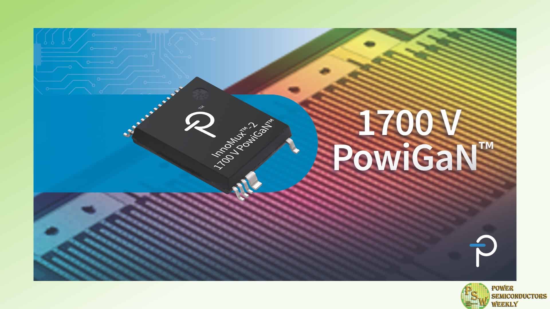
Power Integrations introduced a new member of its InnoMux™-2 family of single-stage, independently regulated multi-output offline power supply ICs. The new device features the industry’s first 1700 V gallium nitride switch, fabricated using the company’s proprietary PowiGaN™ technology.
The 1700 V rating further advances the state-of-the-art for GaN power devices, previously set by Power Integrations’ own 900 V and 1250 V devices, both launched in 2023. The 1700 V InnoMux-2 IC easily supports 1000 VDC nominal input voltage in a flyback configuration and achieves over 90 percent efficiency in applications requiring one, two or three supply voltages.
Each output is regulated within one percent accuracy, eliminating post regulators and further improving system efficiency by approximately ten percent. The new device replaces expensive silicon carbide (SiC) transistors in power supply applications such as automotive chargers, solar inverters, three-phase meters and a wide variety of industrial power systems.
Radu Barsan, vice president of technology at Power Integrations, said, “Our rapid pace of GaN development has delivered three world-first voltage ratings in a span of less than two years: 900 V, 1250 V and now 1700 V. Our new InnoMux-2 ICs combine 1700 V GaN and three other recent innovations: independent, accurate, multi-output regulation; FluxLink™, our secondary-side regulation (SSR) digital isolation communications technology; and zero voltage switching (ZVS) without an active-clamp, which all but eliminates switching losses.”
Original – Power Integrations
-

Navitas Semiconductor will showcase its latest innovations at the 2024 China Power Electronics and Energy Conversion Conference and the 27th Annual Academic Conference and Exhibition of the China Power Supply Society (CPEEC & CPSSC 2024), held in Xi’an from November 8th – 11th, 2024.
At ‘Planet Navitas’ (Booth 3-011), visitors can discover the AI Power Roadmap, which showcases the world’s first 8.5 kW OCP AI data center power supply implementing GaNSafe and Gen-3 Fast SiC MOSFETs, alongside the highest power density 4.5 kW AI data center power supply on the planet. Navitas also developed the ‘IntelliWeave’ patented digital control combined with high-power GaNSafe™ and Gen 3-Fast SiC MOSFETs, optimized for AI data center power supplies, enabling PFC peak efficiencies to 99.3% and reducing power losses by 30% compared to existing solutions.
Additionally, industry-leading solutions include a 6.6kW 2-in-1 EV on-board charger (OBC) utilizing a hybrid GaNSafe and GeneSiC design and fast-charging solutions for consumer electronics with the latest GaNSlim family.
The new GaNSlim family offers a highly integrated GaN solution with autonomous EMI control and loss-less sensing that enables the industry’s fastest, smallest, and most efficient solution in an optimized DPAK-4L package, ideal for mobile, consumer, and home appliance applications up to 500 W.
Enabled by over 20 years of SiC innovation leadership, GeneSiC technology leads on performance with the Gen-3 Fast SiC MOSFETs with ‘trench-assisted planar’ technology. This proprietary technology provides world-leading performance over temperature, delivering cool-running, fast-switching, and superior robustness to support up to 3x more powerful AI data centers and faster charging EVs.
As China’s premier power electronics event, CPSSC gathers industry leaders, researchers, and enterprises to explore breakthrough technologies shaping the future of power electronics. This year’s focus is on high-efficiency, high-power density solutions. “CPSSC is a key platform to showcase Navitas’ role in advancing power electronics,” said Charles Zha, VP & GM of Navitas China. “Our GaNSafe, GaNSlim, and Gen-3 Fast SiC technologies highlight our commitment to enabling higher efficiency, faster charging, and more powerful applications, aligning with CPSSC’s vision of powering the future.”
Navitas will also present technical papers and host industrial sessions, sharing insights into GaN and SiC technologies and their real-world applications.
Navitas’ CPSSC 2024 Program Highlights:
- November 10
- Paper Presentation:
Research on Parasitic False Turn-On Behaviour of SiC MOSFETs with 0V Turn-Off Gate Voltage
13:20-13:40 | Xiangyang Zhou, Bin Li, Xiucheng Huang, Jason Zhang - Industrial Session:
Bi-Directional GaN for Improving Efficiency in Micro-Inverters
14:30-15:00 | Simon Qin, Sr. Staff Application Engineer
- November 11
- Technical Presentation:
Achieving 99.4% Efficiency in GaN-based Interleaving CrM TTP PFC
08:30-09:00 | Wenhao Yu, Sr. Application Engineer - Technology Showcase:
GaNSlim IC: Redefining Efficiency in Cost-Effective Power Supplies
10:20-10:50 | Ye Hu, Technical Marketing Manager - Industry Insights:
Opportunities and Challenges of Single-Stage Converters for On-Board Chargers
13:00-13:30 | Justin Zhu, Sr. Technical Marketing Manager
Original – Navitas Semiconductor
-

Texas Instruments (TI) announced it has begun production of gallium nitride (GaN)-based power semiconductors at its factory in Aizu, Japan. Coupled with its existing GaN manufacturing in Dallas, Texas, TI will now internally manufacture four times more GaN-based power semiconductors, as Aizu ramps to production.
“Building on more than a decade of expertise in GaN chip design and manufacturing, we have successfully qualified our 200mm GaN technology – the most scalable and cost-competitive way to manufacture GaN today – to start mass production in Aizu,” said Mohammad Yunus, TI’s senior vice president of Technology and Manufacturing. “This milestone enables us to manufacture more of our GaN chips internally as we grow our internal manufacturing to more than 95% by 2030, while also sourcing from multiple TI locations, ensuring a reliable supply of our entire GaN portfolio of high-power, energy-efficient semiconductors.”
An alternative to silicon, GaN is a semiconductor material that offers benefits in energy-efficiency, switching speed, power solution size and weight, overall system cost, and performance under high temperatures and high-voltage conditions. GaN chips provide more power density, or power in smaller spaces, enabling applications such as power adapters for laptops and mobile phones, or smaller, more energy-efficient motors for heating and air conditioning systems and home appliances.
Today, TI offers the widest portfolio of integrated GaN-based power semiconductors, ranging from low- to high-voltage, to enable the most energy-efficient, reliable and power-dense electronics.
“With GaN, TI can deliver more power, more efficiently in a compact space, which is the primary market need driving innovation for many of our customers,” said Kannan Soundarapandian, vice president of High-Voltage Power at TI. “As designers of systems such as server power, solar energy generation and AC/DC adapters face challenges to reduce power consumption and enhance energy efficiency, they are increasingly demanding a reliable supply of TI’s high-performance GaN-based chips. TI’s product portfolio of integrated GaN power stages enables customers to achieve higher power density, improved ease of use and lower system cost.”
Further, with the company’s proprietary GaN-on-silicon process, more than 80 million hours of reliability testing, and integrated protection features, TI GaN chips are designed to keep high-voltage systems safe.
Using the most advanced equipment available for GaN chip manufacturing today, TI’s new capacity enables increased product performance and manufacturing process efficiency, as well as a cost advantage. Also, the more advanced, efficient tools used in TI’s expanded GaN manufacturing can produce smaller chips, packing even more power. This design innovation can be manufactured using less water, energy and raw materials, and end products that use GaN chips enjoy these same environmental benefits.
The performance benefits of TI’s added GaN manufacturing also enable the company to scale its GaN chips to higher voltages, starting with 900V and increasing to higher voltages over time, furthering power-efficiency and size innovations for applications like robotics, renewable energy and server power supplies.
In addition, TI’s expanded investment includes a successful pilot earlier this year for development of GaN manufacturing processes on 300mm wafers. Further, TI’s expanded GaN manufacturing processes are fully transferable to 300mm technology, positioning the company to readily scale to customer needs and move to 300mm in the future.
Expanding supply and innovation in GaN technology is the latest example of TI’s commitment to responsible, sustainable manufacturing. TI has committed to use 100% renewable electricity in its U.S. operations by 2027, and worldwide by 2030.
Original – Texas Instruments
-

Many industrial applications today are transitioning to higher power levels with minimized power losses, which can be achieved through increased DC link voltage. Infineon Technologies AG addresses this challenge by introducing the CoolSiC™ Schottky diode 2000 V G5, the first discrete silicon carbide diode on the market with a breakdown voltage of 2000 V. The product family is suitable for applications with DC link voltages up to 1500 VDC and offers current ratings from 10 to 80 A. This makes it ideal for higher DC link voltage applications such as in solar and EV charging applications.
The product family comes in a TO-247PLUS-4-HCC package, with 14 mm creepage and 5.4 mm clearance distance. This, together with a current rating of up to 80 A, enables a significantly higher power density. It allows developers to achieve higher power levels in their applications with only half the component count of 1200 V solutions. This simplifies the overall design and enables a smooth transition from multi-level topologies to 2-level topologies.
In addition, the CoolSiC Schottky diode 2000V G5 utilizes the .XT interconnection technology that leads to significantly lower thermal resistance and impedance, enabling better heat management. Furthermore, the robustness against humidity has been demonstrated in HV-H3TRB reliability tests. The diodes exhibit neither reverse recovery current nor forward recovery and feature a low forward voltage, ensuring enhanced system performance.
The 2000 V diode family is a perfect match for the CoolSiC MOSFETs 2000 V in the TO-247Plus-4 HCC package that Infineon introduced in spring 2024. The CoolSiC diodes 2000 V portfolio will be extended by offering them in the TO-247-2 package, which will be available in December 2024. A matching gate driver portfolio is also available for the CoolSiC MOSFETs 2000 V.
Original – Infineon Technologies
