-
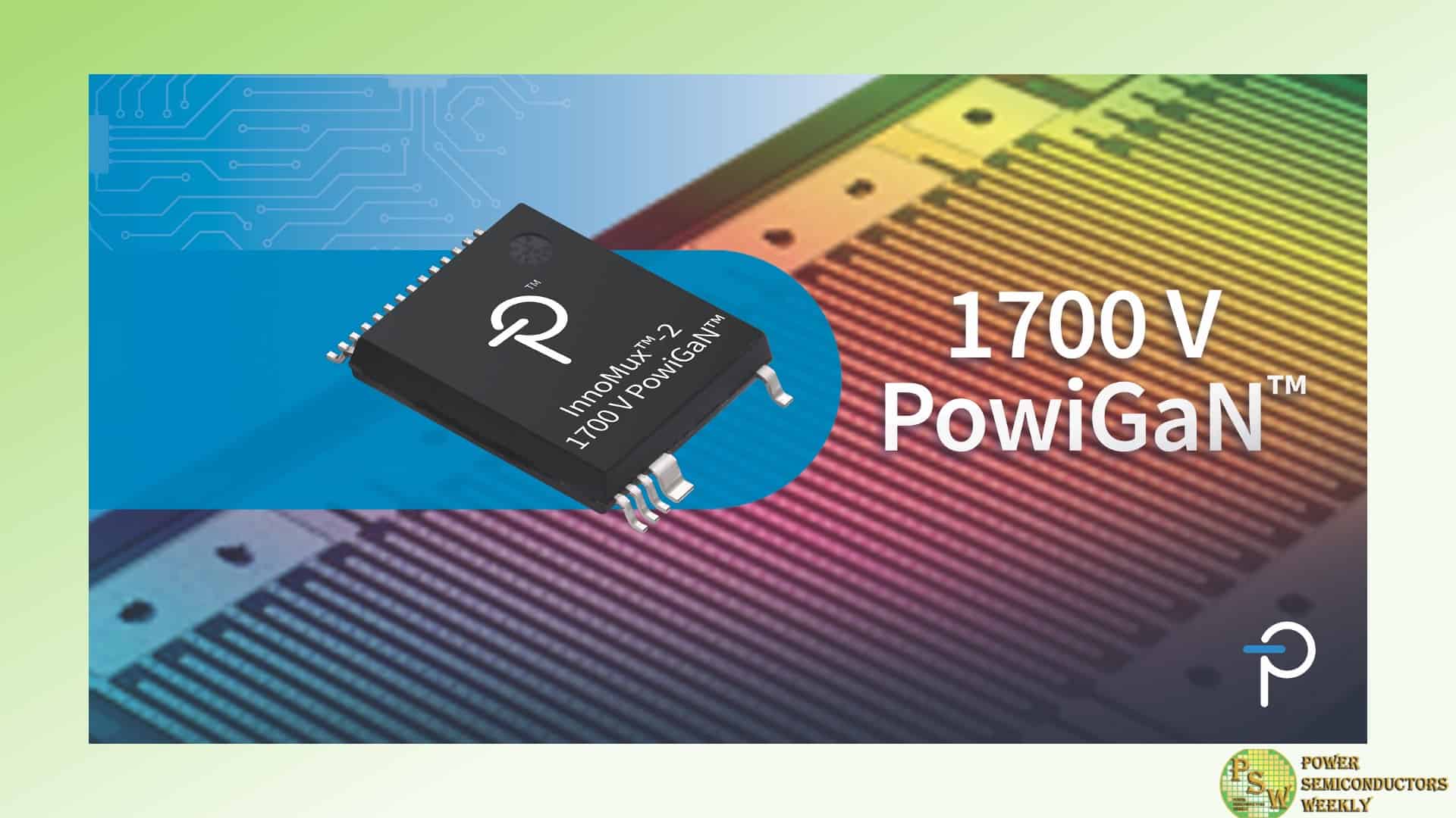
Power Integrations introduced a new member of its InnoMux™-2 family of single-stage, independently regulated multi-output offline power supply ICs. The new device features the industry’s first 1700 V gallium nitride switch, fabricated using the company’s proprietary PowiGaN™ technology.
The 1700 V rating further advances the state-of-the-art for GaN power devices, previously set by Power Integrations’ own 900 V and 1250 V devices, both launched in 2023. The 1700 V InnoMux-2 IC easily supports 1000 VDC nominal input voltage in a flyback configuration and achieves over 90 percent efficiency in applications requiring one, two or three supply voltages.
Each output is regulated within one percent accuracy, eliminating post regulators and further improving system efficiency by approximately ten percent. The new device replaces expensive silicon carbide (SiC) transistors in power supply applications such as automotive chargers, solar inverters, three-phase meters and a wide variety of industrial power systems.
Radu Barsan, vice president of technology at Power Integrations, said, “Our rapid pace of GaN development has delivered three world-first voltage ratings in a span of less than two years: 900 V, 1250 V and now 1700 V. Our new InnoMux-2 ICs combine 1700 V GaN and three other recent innovations: independent, accurate, multi-output regulation; FluxLink™, our secondary-side regulation (SSR) digital isolation communications technology; and zero voltage switching (ZVS) without an active-clamp, which all but eliminates switching losses.”
Original – Power Integrations
-

Navitas Semiconductor will showcase its latest innovations at the 2024 China Power Electronics and Energy Conversion Conference and the 27th Annual Academic Conference and Exhibition of the China Power Supply Society (CPEEC & CPSSC 2024), held in Xi’an from November 8th – 11th, 2024.
At ‘Planet Navitas’ (Booth 3-011), visitors can discover the AI Power Roadmap, which showcases the world’s first 8.5 kW OCP AI data center power supply implementing GaNSafe and Gen-3 Fast SiC MOSFETs, alongside the highest power density 4.5 kW AI data center power supply on the planet. Navitas also developed the ‘IntelliWeave’ patented digital control combined with high-power GaNSafe™ and Gen 3-Fast SiC MOSFETs, optimized for AI data center power supplies, enabling PFC peak efficiencies to 99.3% and reducing power losses by 30% compared to existing solutions.
Additionally, industry-leading solutions include a 6.6kW 2-in-1 EV on-board charger (OBC) utilizing a hybrid GaNSafe and GeneSiC design and fast-charging solutions for consumer electronics with the latest GaNSlim family.
The new GaNSlim family offers a highly integrated GaN solution with autonomous EMI control and loss-less sensing that enables the industry’s fastest, smallest, and most efficient solution in an optimized DPAK-4L package, ideal for mobile, consumer, and home appliance applications up to 500 W.
Enabled by over 20 years of SiC innovation leadership, GeneSiC technology leads on performance with the Gen-3 Fast SiC MOSFETs with ‘trench-assisted planar’ technology. This proprietary technology provides world-leading performance over temperature, delivering cool-running, fast-switching, and superior robustness to support up to 3x more powerful AI data centers and faster charging EVs.
As China’s premier power electronics event, CPSSC gathers industry leaders, researchers, and enterprises to explore breakthrough technologies shaping the future of power electronics. This year’s focus is on high-efficiency, high-power density solutions. “CPSSC is a key platform to showcase Navitas’ role in advancing power electronics,” said Charles Zha, VP & GM of Navitas China. “Our GaNSafe, GaNSlim, and Gen-3 Fast SiC technologies highlight our commitment to enabling higher efficiency, faster charging, and more powerful applications, aligning with CPSSC’s vision of powering the future.”
Navitas will also present technical papers and host industrial sessions, sharing insights into GaN and SiC technologies and their real-world applications.
Navitas’ CPSSC 2024 Program Highlights:
- November 10
- Paper Presentation:
Research on Parasitic False Turn-On Behaviour of SiC MOSFETs with 0V Turn-Off Gate Voltage
13:20-13:40 | Xiangyang Zhou, Bin Li, Xiucheng Huang, Jason Zhang - Industrial Session:
Bi-Directional GaN for Improving Efficiency in Micro-Inverters
14:30-15:00 | Simon Qin, Sr. Staff Application Engineer
- November 11
- Technical Presentation:
Achieving 99.4% Efficiency in GaN-based Interleaving CrM TTP PFC
08:30-09:00 | Wenhao Yu, Sr. Application Engineer - Technology Showcase:
GaNSlim IC: Redefining Efficiency in Cost-Effective Power Supplies
10:20-10:50 | Ye Hu, Technical Marketing Manager - Industry Insights:
Opportunities and Challenges of Single-Stage Converters for On-Board Chargers
13:00-13:30 | Justin Zhu, Sr. Technical Marketing Manager
Original – Navitas Semiconductor
-

Texas Instruments (TI) announced it has begun production of gallium nitride (GaN)-based power semiconductors at its factory in Aizu, Japan. Coupled with its existing GaN manufacturing in Dallas, Texas, TI will now internally manufacture four times more GaN-based power semiconductors, as Aizu ramps to production.
“Building on more than a decade of expertise in GaN chip design and manufacturing, we have successfully qualified our 200mm GaN technology – the most scalable and cost-competitive way to manufacture GaN today – to start mass production in Aizu,” said Mohammad Yunus, TI’s senior vice president of Technology and Manufacturing. “This milestone enables us to manufacture more of our GaN chips internally as we grow our internal manufacturing to more than 95% by 2030, while also sourcing from multiple TI locations, ensuring a reliable supply of our entire GaN portfolio of high-power, energy-efficient semiconductors.”
An alternative to silicon, GaN is a semiconductor material that offers benefits in energy-efficiency, switching speed, power solution size and weight, overall system cost, and performance under high temperatures and high-voltage conditions. GaN chips provide more power density, or power in smaller spaces, enabling applications such as power adapters for laptops and mobile phones, or smaller, more energy-efficient motors for heating and air conditioning systems and home appliances.
Today, TI offers the widest portfolio of integrated GaN-based power semiconductors, ranging from low- to high-voltage, to enable the most energy-efficient, reliable and power-dense electronics.
“With GaN, TI can deliver more power, more efficiently in a compact space, which is the primary market need driving innovation for many of our customers,” said Kannan Soundarapandian, vice president of High-Voltage Power at TI. “As designers of systems such as server power, solar energy generation and AC/DC adapters face challenges to reduce power consumption and enhance energy efficiency, they are increasingly demanding a reliable supply of TI’s high-performance GaN-based chips. TI’s product portfolio of integrated GaN power stages enables customers to achieve higher power density, improved ease of use and lower system cost.”
Further, with the company’s proprietary GaN-on-silicon process, more than 80 million hours of reliability testing, and integrated protection features, TI GaN chips are designed to keep high-voltage systems safe.
Using the most advanced equipment available for GaN chip manufacturing today, TI’s new capacity enables increased product performance and manufacturing process efficiency, as well as a cost advantage. Also, the more advanced, efficient tools used in TI’s expanded GaN manufacturing can produce smaller chips, packing even more power. This design innovation can be manufactured using less water, energy and raw materials, and end products that use GaN chips enjoy these same environmental benefits.
The performance benefits of TI’s added GaN manufacturing also enable the company to scale its GaN chips to higher voltages, starting with 900V and increasing to higher voltages over time, furthering power-efficiency and size innovations for applications like robotics, renewable energy and server power supplies.
In addition, TI’s expanded investment includes a successful pilot earlier this year for development of GaN manufacturing processes on 300mm wafers. Further, TI’s expanded GaN manufacturing processes are fully transferable to 300mm technology, positioning the company to readily scale to customer needs and move to 300mm in the future.
Expanding supply and innovation in GaN technology is the latest example of TI’s commitment to responsible, sustainable manufacturing. TI has committed to use 100% renewable electricity in its U.S. operations by 2027, and worldwide by 2030.
Original – Texas Instruments
-

Many industrial applications today are transitioning to higher power levels with minimized power losses, which can be achieved through increased DC link voltage. Infineon Technologies AG addresses this challenge by introducing the CoolSiC™ Schottky diode 2000 V G5, the first discrete silicon carbide diode on the market with a breakdown voltage of 2000 V. The product family is suitable for applications with DC link voltages up to 1500 VDC and offers current ratings from 10 to 80 A. This makes it ideal for higher DC link voltage applications such as in solar and EV charging applications.
The product family comes in a TO-247PLUS-4-HCC package, with 14 mm creepage and 5.4 mm clearance distance. This, together with a current rating of up to 80 A, enables a significantly higher power density. It allows developers to achieve higher power levels in their applications with only half the component count of 1200 V solutions. This simplifies the overall design and enables a smooth transition from multi-level topologies to 2-level topologies.
In addition, the CoolSiC Schottky diode 2000V G5 utilizes the .XT interconnection technology that leads to significantly lower thermal resistance and impedance, enabling better heat management. Furthermore, the robustness against humidity has been demonstrated in HV-H3TRB reliability tests. The diodes exhibit neither reverse recovery current nor forward recovery and feature a low forward voltage, ensuring enhanced system performance.
The 2000 V diode family is a perfect match for the CoolSiC MOSFETs 2000 V in the TO-247Plus-4 HCC package that Infineon introduced in spring 2024. The CoolSiC diodes 2000 V portfolio will be extended by offering them in the TO-247-2 package, which will be available in December 2024. A matching gate driver portfolio is also available for the CoolSiC MOSFETs 2000 V.
Original – Infineon Technologies
-

Electric drives are becoming increasingly prevalent in the boat and ship sector. At METSTRADE, Bosch Engineering is unveiling a newly developed, high-performance electrification solution for electrical systems with voltages of up to 800 volts, which further extends the potential use cases of electric drives in maritime applications while also raising system efficiency.
“With the latest generation of our electric motor and inverter with silicon carbide power modules, we offer a complete system that allows not only recreational boats but also larger sailing yachts and working boats to be operated with an efficient, quiet, yet still very powerful electric drive,” states Philip Kurek, who is responsible for off-highway and maritime solutions at Bosch Engineering.
The new electric motor SMG 230 is designed for system voltages of 400 to 800 volts. In an ideal voltage and temperature range, it offers a continuous power output of up to 200 kilowatts and around 250 newton meters of torque. Thanks to the 800-volt technology, the power density has also been increased significantly. The SMG 230 delivers 80 kilowatts more power than a comparable 400-volt machine with identical weight or, with the same level of performance, boasts more compact dimensions and a much lower weight.
The inverter with silicon carbide semiconductors, which is also designed for electrical voltages of up to 800 volts, is characterized by its impressive efficiency of more than 99 percent. The silicon carbide semiconductors in the power modules enable faster switching operations, meaning that significantly less energy is lost in the form of heat.
Bosch’s complete kit for the electrification of boat drives comprises electronic control units, inverters, electric motors, and transmissions for both 400- and 800-volt applications. This gives shipyards and system integrators maximum flexibility when adapting the electrification strategy to the respective requirements and allows them to integrate the relevant components quickly and easily into their ships. The system components are based on modern automotive technology and combine high robustness with utmost reliability. With its comprehensive kit for the electrification of ship drives, Bosch is making a crucial contribution to the ongoing reduction of greenhouse gas and noise emissions.
Original – Bosch
-

At this month’s IEEE Energy Conversion Congress and Expo (ECCE), Navitas Semiconductor introduced conference attendees to ‘IntelliWeave’ – an innovative patented new digital control technique for improving next generation AI data center power supply (PSU) efficiency.
In a world where ever-more energy is needed for the processing of artificial intelligence (AI) and cloud-based applications, minimizing power consumption has become a priority for data center architects and operators. Combining next-generation GaN and SiC semiconductors with new control technique strategies to power conversion plays a key role in achieving this goal.
IntelliWeave’s novel digital control enables highest system efficiencies with precision current sharing, ultra-fast dynamic response and minimal phase error. A patented dual-loop and dual-feed-forward interleaving control achieves absolute zero voltage switching (ZVS) across the full-load range to enable highest efficiencies.
The digital control for Critical Conduction Mode (CRM) interleaving Totem Pole Power Factor Control (PFC) enables 30% reduction in power losses compared to existing Continuous Conduction Mode (CCM) solutions. The digital control combined with high-power GaNSafe power ICs has been proven on a 500 kHz GaN-based interleaving 3.2 kW CrM PFC PSU operating at 99.3% peak efficiency including EMI filter loss.
Taking place in Phoenix, Arizona from October 20th to 24th, IEEE ECCE 2024 features both industry-driven and application-oriented technical sessions and brings together practicing engineers, researchers and other professionals for interactive and multidisciplinary discussions on the latest advances in various areas related to energy conversion.
On October 21st Tao Wei presented “Novel digital control for a GaN-based CrM interleaved TP PFC”.
Original – Navitas Semiconductor
-

Affordability combined with high performance and efficiency is the key to making electric mobility accessible to a broader market. That’s why Infineon Technologies AG is introducing the HybridPACK™ Drive G2 Fusion, establishing a new power module standard for traction inverters in the e-mobility sector.
The HybridPACK Drive G2 Fusion is the first plug’n’play power module that implements a combination of Infineon’s silicon and silicon carbide (SiC) technologies. This cutting-edge solution provides an ideal balance between performance and cost efficiency, giving more choice in the optimization of inverters.
One of the main differences between silicon and SiC in power modules is that SiC has a higher thermal conductivity, breakdown voltage and switching speed, making it more efficient, but also more expensive than silicon-based power modules. With the new module, the SiC content per vehicle can be reduced, while maintaining vehicle performance and efficiency at a lower system cost. For example, system suppliers can realize nearly the system efficiency of a full SiC solution with only 30 percent SiC and 70 percent silicon area.
“Our new HybridPACK Drive G2 Fusion module underlines Infineon’s innovation leadership in the automotive semiconductor industry,” said Negar Soufi-Amlashi, Senior Vice President & General Manager High Voltage at Infineon’s Automotive division. “Addressing the demand for greater e-mobility range, this technological breakthrough smartly combines silicon carbide and silicon. Integrated in a well-introduced module package footprint it offers compelling cost-performance ratio over pure silicon carbide modules without adding system complexity for automotive system suppliers and vehicle manufacturers.”
HybridPACK Drive G2 Fusion expands Infineon’s HybridPACK Drive power module portfolio and can be quickly and easily integrated in vehicle components or modules without requiring complex adjustments or configurations. The HybridPACK Drive G2 Fusion module features up to 220 kW in the 750 V class. It ensures high reliability over the entire temperature range from -40 °C to +175 °C and improved thermal conductivity.
The unique properties of Infineon’s CoolSiC™ technology and its silicon IGBT EDT3 technology with very fast turn-on enable the use of a single gate driver or dual gate drivers. This allows easy re-design from full silicon or full SiC based inverters to a fusion inverter. Generally, Infineon’s holistic expertise in SiC MOSFET and silicon IGBT technology, power module packaging, gate drivers as well as sensors enables premium products with cost savings at system level. One example is the integration of Swoboda or XENSIV™ Hall sensors in the HybridPACK Drive package for more precise and efficient motor control.
Infineon will showcase the new HybridPACK Drive G2 Fusion at electronica 2024 in Munich from November 12 to 15 (hall C3, booth 502).
Original – Infineon Technologies
-

The U.S. Department of Commerce and Wolfspeed announced they have signed a non-binding preliminary memorandum of terms (PMT) for up to $750 million in proposed direct funding under the CHIPS and Science Act. In addition, a consortium of investment funds led by Apollo, The Baupost Group, Fidelity Management & Research Company and Capital Group have agreed to provide Wolfspeed an additional $750 million of new financing.
Together these investments support Wolfspeed’s long-term growth plans and bolster domestic production of silicon carbide to power clean energy systems underpinning electric vehicles (EVs), artificial intelligence (AI) data centers, battery storage and more. In addition, Wolfspeed expects to receive $1 billion of cash tax refunds from the advanced manufacturing tax credit under the CHIPS and Science Act (section 48D), giving the company, in total, access to up to $2.5 billion of expected capital to support the expansion of silicon carbide manufacturing in the United States.
Wolfspeed is the world’s largest producer of silicon carbide technology, pioneering the technology more than 35 years ago on the campus of North Carolina State University. Since that time, Wolfspeed has become the global leader in silicon carbide technology, one of the fastest growing components of the broader semiconductor industry.
- Silicon carbide is a superior alternative to silicon for high power applications – such as EV powertrains, e-mobility, renewable energy systems, battery energy storage systems, and AI and cryptocurrency data centers – that unlocks improved performance and lower system costs.
- Notably, the importance of bolstering the domestic production of silicon carbide has been recognized across multiple federal agencies; the Department of Energy denoted it as one of 17 “critical materials” with a high risk of supply disruption that are integral to clean energy technologies, while the Department of Commerce recognizes silicon carbide semiconductors as important to national security.
- As the U.S. and the world pursue more efficient and environmentally friendly solutions to meet the world’s ever-increasing need for high-voltage energy products, it is crucial that the U.S. continue to make strategic investments to cement its technological leadership position, while continuing to spur American innovation in critical technologies.
Wolfspeed CEO, Gregg Lowe, said, “To reach this milestone under the U.S. CHIPS and Science Act is an incredible achievement in Wolfspeed’s long-term growth strategy, and we believe today’s announcement is a testament to the market-leading quality of Wolfspeed products and significance of Wolfspeed to broader U.S. economic and national security interests. This support galvanizes our ability to expand domestic manufacturing, accelerate innovation in next-generation semiconductor technology, and meet the increasing global demand for silicon carbide. As a key player in the semiconductor industry, this proposed investment will enable us to solidify our leadership position with a first-of-its-kind 200mm silicon carbide manufacturing footprint in upstate New York and central North Carolina, while contributing to the resilience and competitiveness of the U.S. supply chain. It’s not just about growth for Wolfspeed—it’s about driving technological advancement that powers the future.
“Silicon carbide is already enabling superior energy efficiency across mission-critical industries of the future like electric vehicles, e-mobility, solar and wind energy, industrial power applications, and AI data centers. While EVs have been the driver of silicon carbide adoption thus far, we believe the use cases for our technology are expansive and will only continue to grow as more and more industries find themselves needing to solve for the same power loss, system size, and system cost challenges as automakers,” concluded Lowe.
“Artificial intelligence, electric vehicles, and clean energy are all technologies that will define the 21st century, and thanks to proposed investments in companies like Wolfspeed, the Biden-Harris Administration is taking a meaningful step towards reigniting U.S. manufacturing of the chips that underpin these important technologies,” said U.S. Secretary of Commerce Gina Raimondo. “Because of the Biden-Harris Administration’s CHIPS and Science Act, the United States is building and fortifying our semiconductor manufacturing capabilities to serve our economic and national security interests while creating jobs and economic opportunities for communities across the country.”
“Wolfspeed is leading the pack in bringing semiconductor manufacturing back to America. This major multibillion dollar investment powered by my CHIPS & Science Law will accelerate the ongoing expansion in the Mohawk Valley, helping speed up hiring of hundreds of new good-paying jobs that Wolfspeed is creating in the Mohawk Valley and providing long term work for the Marcy fab to succeed well into the future, further establishing Upstate NY as a global hub for chip manufacturing,” said Senator Chuck Schumer. “From electric vehicles to artificial intelligence, this critical technology relies on the silicon carbide chips that Wolfspeed will manufacture and perfect in the Mohawk Valley. Today’s massive investment will make America’s economy and our national security stronger as Wolfspeed helps us write the next chapter of America’s resurgence as the leader in the semiconductor industry, with the Mohawk Valley as the beating heart.”
“Wolfspeed is a homegrown semiconductor innovator and manufacturer creating great jobs in North Carolina, and it’s important they received this major grant under the CHIPS and Science Act,” said North Carolina Governor Roy Cooper. “Thanks to this landmark legislation from the Biden-Harris Administration and our great workforce, we will continue to see good paying jobs coming to North Carolina.”
“This $750 million federal investment is a testament to Wolfspeed’s unique leadership in silicon carbide semiconductor manufacturing, and I applaud Wolfspeed’s continued commitment to North Carolina,” said Senator Thom Tillis. “I was proud to vote for the CHIPS and Science Act to provide the funding for this investment in North Carolina and to support our economic and national security.”
“North Carolina continues to be a leader in cutting-edge manufacturing that is vital to our country’s national and economic security,” said Senator Ted Budd. “This new Wolfspeed site in Siler City will bring good-paying jobs to the area and is an important first step in making sure America has secure supply chains for critical semi-conductors.”
“We are pleased to expand our investment in Wolfspeed by providing additional capital in support of the company’s build out of its leading silicon carbide capabilities,” said Apollo Partner Joseph Jackson. “We believe Wolfspeed is at the forefront of a critical transformation in sustainable transportation and ensuring that the company has durable capital access to complete its expansion plans will help solidify its leadership in this space. Along with our lending consortium, which includes multiple funds that also own substantial equity stakes in the company, we believe this strategic investment will drive significant long-term value while advancing key tenets of the CHIPS and Science Act.”
These proposed funds, which are expected to be received upon milestone achievements in the coming years, would enable Wolfspeed to complete its multi-billion-dollar greenfield U.S. capacity expansion plan, which consists of the largest and most advanced 200mm silicon carbide footprint in the world. In addition to the proposed direct funding, Wolfspeed intends to benefit from the U.S. Treasury Department Investment Tax Credit of up to 25% of the qualified capital expenditures primarily related to its construction and installation of equipment at The John Palmour Manufacturing Center for Silicon Carbide in Siler City, NC and completion of the Mohawk Valley Fab M-Line West Expansion in Utica, NY.
This multi-billion-dollar investment will bolster Wolfspeed’s balance sheet and will help to fuel significant growth through cash generation and accelerate its long-term profitability goals.
Summary of the PMT
The PMT outlines key terms for a CHIPS incentive award, including the proposed amount and form of the award, and provides that the disbursement of funds will be conditioned upon the achievement of certain operational and construction milestones and other requirements.
The PMT includes an obligation for Wolfspeed to raise an aggregate of $750 million in debt financing over three tranches through the issuance of senior notes under an amended and restated indenture. Wolfspeed and its lenders, led by Apollo funds, have reached an agreement for this additional financing, including $250 million to be available within 10 business days, and have agreed to certain intercreditor terms with the CHIPS Program Office as described in the PMT.
Together, the PMT and the agreement with lenders also requires:
- Wolfspeed to undertake further actions with respect to its capital structure, including (a) restructuring or refinancing its outstanding 2026, 2028 and 2029 convertible notes at specified intervals prior to their respective maturity dates, (b) deferring a total of $120 million in cash interest payments due prior to June 30, 2025 under an unsecured customer refundable deposit agreement, and (c) raising up to $300 million of additional capital from non-debt sources over the next 12 months.
- In addition, Wolfspeed has agreed with its lenders to certain revisions in the terms of the senior notes, including revisions to the interest rate applicable to the senior notes, as described in the Form 8-K filed today with Securities and Exchange Commission (SEC).
The PMT provides that the award is subject to due diligence and the negotiation and signing of a definitive direct funding agreement with the Department of Commerce and the negotiation and signing of an intercreditor agreement between the Department of Commerce and the Company’s lenders, which may contain different or additional conditions not contained in the PMT. Additional terms of the PMT were not disclosed.
Original – Wolfspeed
-

Navitas Semiconductor announced GaNSlim™, a new generation of highly-integrated GaN power ICs that will further simplify and speed the development of small form factor, high-power-density applications by offering the highest level of integration and thermal performance.
GaNSlim enables the simplest, fastest, and smallest system design by integrating drive, control, and protection, with integrated EMI control and loss-less current sensing, all within a high thermal performance proprietary DPAK-4L package. Additionally, with an ultra-low startup current below 10 µA, GaNSlim devices are compatible with industry-standard SOT23-6 controllers and eliminate HV startup.
Integrated features such as loss-less current sensing eliminate external current sensing resistors and optimize system efficiency and reliability. Over-temperature protection ensures system robustness and auto sleep-mode increases light and no-load efficiency. Autonomous turn-on/off slew rate control maximizes efficiency and power density while reducing external component count, system cost and EMI.
GaNSlim features a patented, 4-pin, high-thermal-performance, low-profile, low-inductance, DPAK package. This package enables 7 °C lower temperature operation versus conventional alternatives, supporting high-power-density designs with ratings up to 500 W. Target applications include chargers for mobile devices and laptops, TV power supplies, lighting, etc.
“Our GaN focus is on integrated devices that enable high-efficiency, high-performance power conversion with the simplest designs and the shortest possible time-to-market,” says Reyn Zhan, Sr. Manager of Technical Marketing. “Our new GaNSlim portfolio – built on integration, ease-of-use, and low-cost manufacturing methods, – continues to grow the customer pipeline with over 50 new projects already identified. GaNSlim increases our GaN addressable market by enabling lower system costs compared to silicon designs for many applications, targeting applications under 500 W across mobile, consumer and home appliance.”
Devices in the NV614x GaNSlim family are rated at 700 V with RDS(ON) ratings from 120 mΩ to 330 mΩ and are available in versions optimized for both isolated and non-isolated topologies.
As with other Navitas GaN ICs, GaNSlim devices are supplied with an industry-leading twenty-year warranty, while demo boards for QR flyback, single-stage PFC, boost PFC plus QR flyback and TV power supply designs allow for rapid evaluation and selection of the optimum device for a given application.
Original – Navitas Semiconductor
-

Infineon Technologies AG announced a partnership with Canada-based AWL-Electricity Inc., a pioneer in MHz resonant capacitive coupling power transfer technology. Infineon provides AWL-E with CoolGaN™ GS61008P allowing the development of advanced wireless power solutions, enabling new ways to solve power challenges in various industries.
The partnership combines Infineon’s cutting-edge gallium nitride (GaN) technology with AWL-E’s innovative MHz resonant capacitive coupling power transfer system, achieving industry-benchmark wireless power efficiencies. Infineon’s GaN transistor technology offers highest efficiency and highest power density while operating at highest switching frequencies.
This enables AWL-E to increase its system lifetime, reduces downtime and operating costs, and improves ease-of-use for consumers. In the automotive sector, the technology enables a new level of interior experiences and seat dynamics. In industrial systems, it provides near-unconstrained levels of design freedom, such as for automated guided vehicles or robotic applications. Additionally, the technology allows for a fully sealed system design, eliminating the need for charging ports which contributes to reducing global consumption of batteries.
“With our partner approach we prove once more the ability to unlocking the full system-level benefits of Infineon’s CoolGaN technology, enabling compactness and efficiency,” said Falk Herm, Global Partnership & Ecosystem Management at Infineon’s Power & Sensor Systems (PSS) Division at Infineon. “The combination of AWL-E and Infineon’s complementary capabilities demonstrates how the features of GaN, namely operating at MHz frequencies, change the paradigm of what can be done with power transistors, driving greener and better performing products.”
“Infineon uniquely brings you into their family with a recognition that a strong ecosystem ultimately solves today’s power needs,” said Francis Beauchamp-Verdon, Co-founder, VP and Business Development Director at AWL-E. “Infineon’s GaN transistors, eval boards, and partner opportunities have boosted acceptance of our GaN-based MHz power coupling systems.”
Infineon is a leader in the power semiconductor market and currently the only manufacturer mastering all power technologies while offering the broadest product and technology portfolio of silicon (such as SJ MOSFETs, IGBTs), silicon carbide (such as Schottky diodes and MOSFETs) and gallium-nitride-based (e-mode HEMT) devices, covering bare die, discretes, and modules.
Original – Infineon Technologies
