-
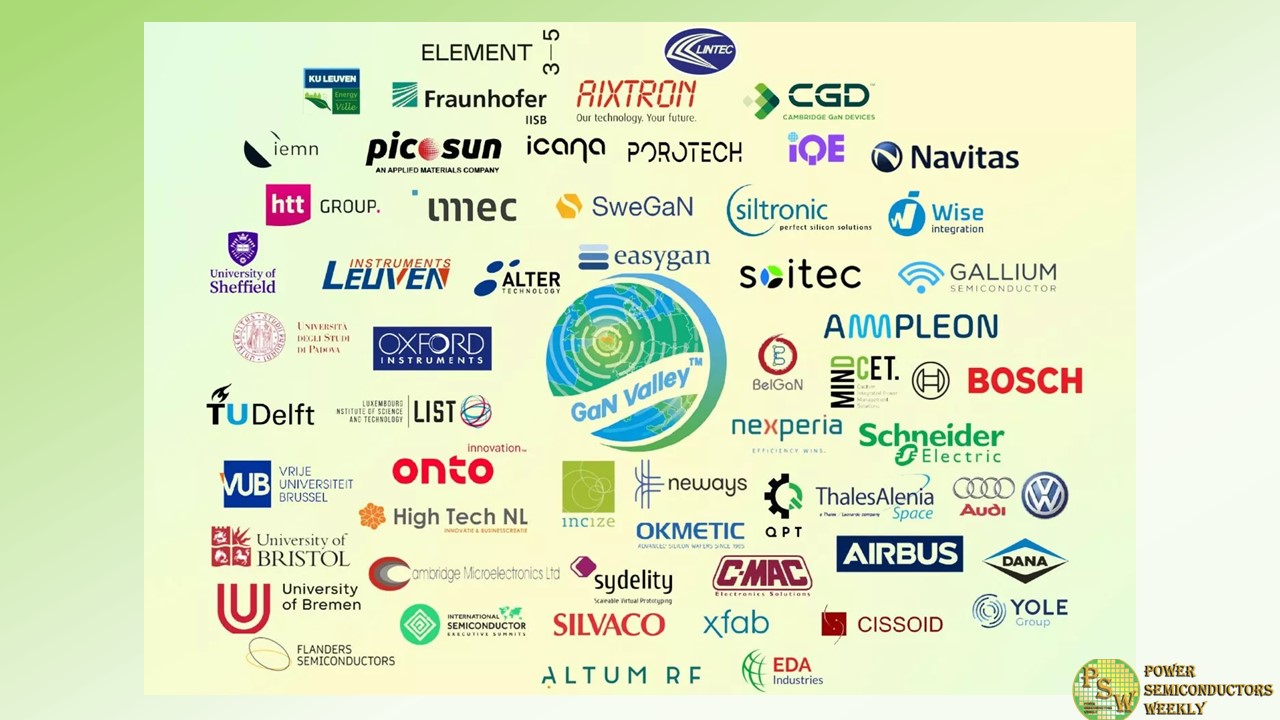
GaN Valley™ is a connected ecosystem along the value chain of GaN technologies, products and electrical systems. It spans research and innovation (such as top-notch universities & RTOs), IDMs, Fabless Companies (including a growing industry of GaN start-ups & scale-ups), GaN Foundries, multi-market customers, as well as various Government Innovation instances.
Okmetic is now a part of GaN Valley™ community and looks forward to cooperation with other members in the GaN ecosystem!
Okmetic supplies substrate wafers for both RF and Power GaN devices. Its silicon substrate wafers are designed to endure the demanding GaN epitaxial process conditions and provide reduced wafer bow and warpage.
Original – Okmetic
-
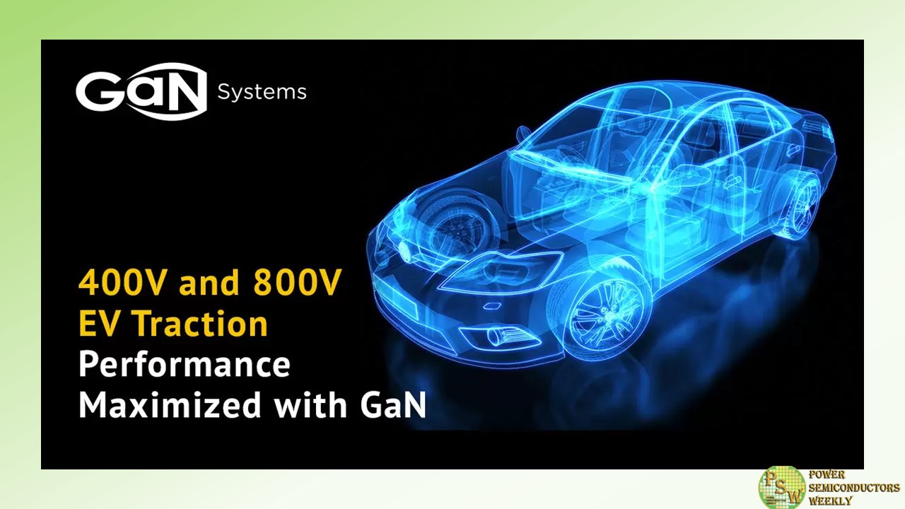
In the world of electric vehicles (EVs), performance and efficiency are paramount. As the EV industry grows, power designers constantly strive to provide more power, reduce losses, minimize heat, and shrink system sizes. These requirements stem from the ongoing pursuit of lighter vehicles with extended ranges, reduced battery size, and lower overall system costs.
The continuous drive for improvement has led to accelerated adoption of a pivotal technology transforming the landscape of EV traction design: Gallium Nitride (GaN). Particularly noteworthy are the benefits of GaN in 400V and 800V battery traction inverter designs. The growing recognition of GaN’s exceptional performance, compared to conventional silicon and SiC alternatives, underscores its critical role in the future of the EV industry.
GaN-Powered 400V Battery Traction Inverters
GaN stands out as a transformative force for 400V battery-based traction inverters—delivering the benefits that designers expect. With GaN, efficiency increases, resulting in nearly 40% reduction in power loss. Additionally, GaN power semiconductors enable a 33% increase in power density, reducing the overall size and weight of the traction inverter. Altogether, the reduced losses and smaller size result in EVs with lower costs and longer driving range, meeting critical consumer requirements.
GaN’s Emergence in 800V Battery Traction Inverters
In 800V battery-based traction inverters, the adoption of GaN-based three-level topology (3LT) is a growing trend. The demonstrated benefits are numerous.
- Higher Overall Efficiency: In addition to minimizing switching losses and increasing efficiency in the inverter, the GaN 3LT solution also reduces high-frequency copper and iron losses in the filters and motor. The inverter plus motor combined efficiency gains translates to incrementally higher efficiency compared to two-level solutions.
- Lower Noise, Harshness, and EMI Interference: The GaN 3LT generates an output voltage with a sinusoidal-like shape, resulting in reduced dV/dt and lower harmonics. The 3LT output reduces filtering requirements and minimizes high-frequency losses in filters and motors, resulting in lower noise, vibration, and harshness (NVH) characteristics. It also operates with a low common voltage, reducing insulation stress and electromagnetic interference (EMI).
- Increased Durability and Reliability: Operating at a lower common voltage also means the peak common mode voltage is suppressed, which reduces the potential for common mode voltage spikes, ensuring a smoother and more stable circuit operation. Furthermore, the 3LT decreases the strain on electric motor bearings. These operating characteristics contribute to a prolonged lifespan with increased durability and reliability.
The EV Market
EVs are at their tipping point, with more than 10 million electric cars sold worldwide in 2022, and sales are expected to grow by 35% this year to reach 14 million cars. Meeting consumer, regulatory, and OEM expectations means peak performance is critical, and this requires a holistic approach that factors in both the inverter and motor considerations. Multi-level GaN is emerging as the lynchpin, offering a range of advantages. Notably, GaN fosters high efficiency at the system level while bolstering overall system reliability.
For example, consider the all-GaN vehicle developed in collaboration with Toyota and Nagoya University teams. The All GaN Vehicle features multiple power applications of GaN in the car: in the traction inverter, the On-Board Charger (OBC), and the DC-DC converter. GaN increased power density and improved efficiency by 20% over silicon, extending the car’s driving range.
Meanwhile, Ricardo, a highly regarded global engineering firm, designed and compared a GaN inverter to a SIC-based inverter. Their test results of the 30kW inverter application demonstrated a 25% reduction in power loss and a 33% increase in power density with GaN compared to SiC. Several Tier1 and OEM automotive companies have realized similar results with traction designs up to 250kW.
In an era of EV innovation, GaN is a driving force accelerating performance and efficiency in both 400V and 800V traction inverters. With the EV industry advancing towards worldwide mass acceptance, the time for GaN adoption is now. The compelling results from rigorous testing and real-world applications point to GaN as the technology well-positioned to reshape the electric mobility landscape.
Original – GaN Systems
-

Navitas Semiconductor announced its continued sponsorship of the 2023 China Power Electronics and Energy Conversion Congress & the 26th China Power Supply Society (CPSS) Conference and Exhibition (CPSSC 2023), revealing major next-generation gallium nitride (GaN) and silicon carbide (SiC) power semiconductor platforms, including GaNSafe™ – the world’s safest GaN power semiconductor.
Hosted in Guangzhou from November 10th-13th, CPSSC 2023 celebrates its 40th anniversary and promotes academic and technical exchange in the fields of power electronics, energy conversion, and power technology, to foster technical innovation and related industries.
Navitas is the technology and market leader in GaN, with over 100 million GaNFast™ power ICs shipped, and over 12 million GeneSiC™ power MOSFETs and diodes shipped into a $22 billion per year total market opportunity.
With GaNSafe, Navitas has optimized its 4th-generation GaN technology for demanding, high-power applications in data centers, solar / energy storage and EV markets, where efficiency, power density and robust & reliable operation are critical. Adopting a novel, robust, and cool-running surface-mount TOLL package, GaNSafe integrates features and functions, including:
- Protected, regulated, integrated gate-drive control, with zero gate-source loop inductance for reliable high-speed 2 MHz switching to maximize power density.
- High-speed short-circuit protection, with autonomous ‘detect and protect’ within 50 ns – 4x faster than competing discrete solutions.
- Electrostatic discharge (ESD) protection of 2 kV, vs. zero for discrete GaN transistors.
- 650/ 800 V capability to aid survival during extraordinary application conditions.
- Easy-to-use, complete, high-power, high-reliability, high-performance power IC with only 4 pins, accelerating customer designs.
- Programmable turn-on and turn-off (dV/dt) to simplify EMI regulatory requirements.
Navitas’ CPSSC 2023 program includes comprehensive, in-depth technology, application and market presentations include a plenary keynote speech, full conference paper, four industrial sessions, a guest PSMA presentation, an in-depth 3.5-hour technology seminar and full GaNSafe launch. Visitors to the exhibition will discover ground-breaking technology demonstrations and complete power system platform designs at the Navitas booth.
Original – Navitas Semiconductor
-
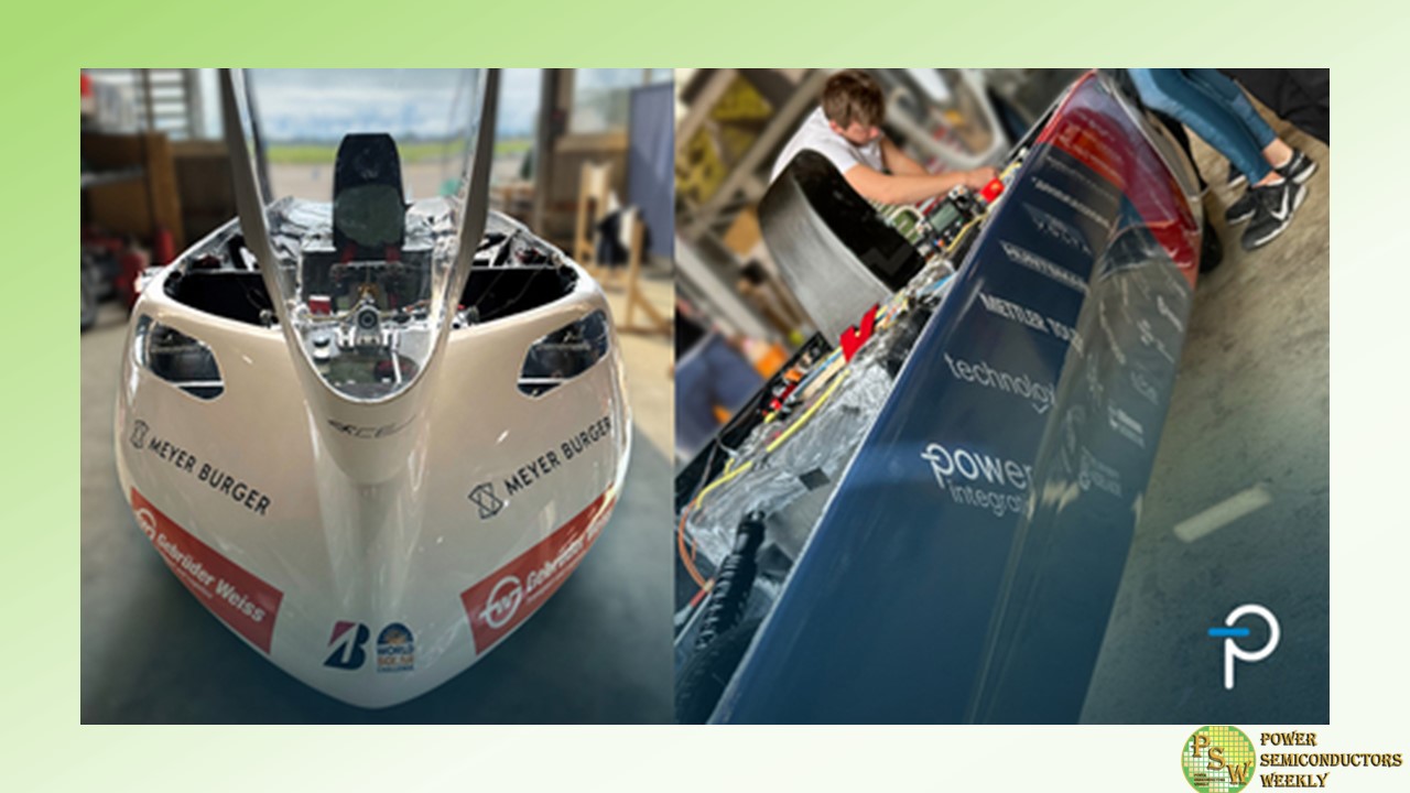
Power Integrations™ is providing advanced PowiGaN™ gallium-nitride (GaN) technology, expert design support, and financial sponsorship for Team aCentauri in the 3,000 km Bridgestone World Solar Challenge later this month. Power Integrations’ Mr. Green will follow Team aCentauri and the 37 other entrants across the Australian Outback as they push the boundaries of innovation in efficiency, aerodynamics, speed and range for solar-powered cars.
“After studying Power Integrations’ extensive list of reference designs, Team aCentauri asked us to help them design a power converter based on the 750-volt, InnoSwitch™3-EP with PowiGaN technology,” said Trevor Hiatt, director of marketing at Power Integrations. “With our IC and expert design support, the team not only boosted energy efficiency to 95.7 percent while the system operates at maximum power, but also improved efficiency by more than 50 percent while the system drives light loads – which is most of the time.”
The Bridgestone World Solar Challenge begins in Darwin on October 22 and is expected to conclude in Adelaide on October 29.
Original – Power Integrations
-

GlobalFoundries has been awarded $35 million in federal funding from the U.S. government to accelerate the manufacturing of GF’s differentiated gallium nitride (GaN) on silicon semiconductors at its facility in Essex Junction, Vermont. This funding brings GF closer to large-scale production of GaN chips, which are unique in their ability to handle high voltages and temperatures.
These chips are positioned to enable game-changing performance and efficiency in 5G and 6G cellular communications for infrastructure and handsets, automotive and industrial Internet of things (IoT), as well as power grids and other critical infrastructure.
With the new $35 million in funding, awarded by the Department of Defense’s Trusted Access Program Office (TAPO), GF plans to purchase additional tools to expand development and prototyping capabilities, moving closer to at-scale 200mm GaN-on-silicon semiconductor manufacturing.
As part of the investment, GF plans to implement new capabilities for reducing the exposure of GF and its customers to supply chain constraints of gallium, while improving the speed of development, assurance of supply and competitiveness of U.S-made GaN chips.
The funding builds on years of collaboration with the U.S. government – including $40 million in support from 2020-2022 – that leverages the talent of GF’s Vermont team and their 200mm semiconductor manufacturing experience, and applies it to GaN-on-silicon manufacturing. 200mm is state-of-the-art for GaN chip technology.
“Vermont is a leader in semiconductor innovation. This federal funding is welcome news, and will solidify our state’s position as a leader at the forefront of manufacturing next-generation chips,” said Senator Peter Welch. “It’s critical we support investment in this industry here in Vermont and in the U.S. – both for our local economic growth and for our national security. I look forward to continuing to fight for our domestic semiconductor and chip manufacturers in the Senate.”
“This strategic investment continues to strengthen our domestic ecosystem of critical dual-use commercial technologies, ensuring they’re readily available and secure for DoD utilization. In concert with key partners, we’re proactively shaping the future of our defense systems,” said The Honorable Christopher J. Lowman, Assistant Secretary of Defense for Sustainment.
“GaN on silicon is an ideal technology for high performance radio frequency, high voltage power switching and control applications for emerging markets, and it’s important for 6G wireless communications, industrial IoT, and electric vehicles,” said Dr. Thomas Caulfield, president and CEO of GF.
“GF has a longstanding partnership with the U.S. government, and this funding is critical to move GaN on silicon chips closer to volume production. These chips will enable our customers to realize bold new designs that push the envelope of energy efficiency and performance of critical technologies we rely on every day.”
GF’s facility in Essex Junction, Vermont, near Burlington, was among the first major semiconductor manufacturing sites in the United States. Today around 1,800 GF employees work at the site. Built on GF’s differentiated technologies, these GF-made chips are used in smartphones, automobiles, and communications infrastructure applications around the world.
The facility is a DMEA accredited Trusted Foundry and manufactures secure chips in partnership with the U.S. Department of Defense, for use in some of the nation’s most sensitive aerospace and defense systems.
Original – GlobalFoundries
-

EPC Space announces the Grand Opening of their new facility in Andover, Massachusetts. Guests are invited to join the EPC Space team for a day of activities that will explore the possibilities that GaN presents to significantly outperform silicon-based devices and enable higher power densities, higher efficiencies, and more compact and lightweight circuitry for critical spaceborne missions.
Radiation hardened (rad hard) GaN improves the performance of power supplies for satellites and space mission equipment, motor drives for robotics, instrumentation and reaction wheels, lidar for autonomous navigation and docking, and deep space probes.
Event Highlights
- Start the day with a warm welcome and enjoy a welcome reception. Guests will receive drink tickets for the upcoming Cocktail Reception and an automatic entry into an exciting raffle.
- Get a glimpse into EPC Space’s remarkable journey and accomplishments as CEO, Bel Lazar, officially opens the event.
- Witness the ceremonial opening of our new facility.
- Explore our facility with guided tours. Immerse yourself in a product showcase and demonstrations, featuring a dedicated Applications table hosted by EPC Space engineers. They will be available to answer questions and demonstrate real-world applications such as DC-DC, POL, and motor control.
- Book Signing by Dr. Alex Lidow (2:30 PM – 3:30 PM): Take this opportunity to meet with Dr. Alex Lidow, CEO of EPC, and author of “GaN Power Devices and Applications,” who will be available to sign copies.
- Connect with EPC Space experts for personalized discussions and insights into rad hard GaN technology.
- Enter for a chance to win exciting prizes during the raffle.
- Network with fellow attendees and the EPC Space team during the Cocktail Reception.
To attend send an RSVP by October 18, 2023 to info@epc.space
“EPC Space is proud to be at the forefront of providing radiation hardened GaN solutions for power conversion to the aerospace industry and beyond,” said Bel Lazar, CEO of EPC Space. “We are happy to invite our customers and partners to be a part of this event and see first-hand how our technology is shaping the future of high reliability applications”.
Original – EPC Space
-

Queensland Semiconductor Technology (Quest) announced opening of its new sales, marketing, assembly and test facility in Coolum Beach. Based very close to the Sunshine Coast airport Quest is now able to ship its power semiconductors to the Australia domestic market. With the airport located within 5 minutes international shipping is swift.
Queensland Semiconductor Technology Pty Ltd stands as a beacon in the semiconductor industry, having established its foundation in Queensland. Quest offers high voltage switching SiC SBD technology that is paramount for transformative applications like electric vehicles, wind farms, and solar power generation. Additionally, product portfolio expands to SiC Mosfets, IGBTs, TCIGBTs & super junction Gan technology plus.
Original – Queensland Semiconductor Technology
-
With decades of expertise in power device packaging and testing, JCET Group offers a comprehensive power product portfolio encompassing IGBT, SiC, GaN, and more. In the field of high-density power solutions for automotive applications, JCET’s unique power module technology positions us at the forefront of power main drive solutions.
JCET’s innovative packaging technology for high power density Silicon Carbide (SiC) power modules minimizes parasitic effects and thermal resistance, while our groundbreaking interconnect technology ensures high reliability. Reduced power loss and improved performance, making JCET the preferred choice for high-reliability SiC device packaging for the automotive industry.
The rapid growth of the power semiconductor market in automotive applications is being driven by the acceleration of vehicle electrification. In this evolving landscape, a multitude of power devices find applications in crucial automotive systems such as motor control, DC-DC conversion, air conditioning drives, on-board chargers (OBC), and battery management for electrical vehicles.
According to research by Strategy Analytics, the value of power devices in battery electric vehicles (BEVs) is nearly five times that in traditional fuel vehicles. This is where SiC devices come into play, offering several advantages. SiC devices feature smaller conductor resistors per unit area, higher voltage capabilities, faster switching speeds, and the ability to operate at high temperatures. These characteristics are instrumental in enhancing the power density of the inverter, ultimately leading to improved operational efficiency and extended mileage for electric vehicles under real-world conditions.
JCET combines low stray inductance package technology, advanced interconnect packaging technology, and cutting-edge thermal management solutions, tailoring our packaging processes to meet individual customer requirements. Within this package, a suite of integrated solutions, including the whole-silver sintering process, copper wire bonding, and single-side direct water cooling, is employed.
Furthermore, SiC devices, with their smaller footprint, increased power density, and higher breakdown voltage compared to conventional silicon-based power devices, are at the core of our packaging. When integrated into an 800V platform, SiC devices deliver substantial system advantages, enabling rapid charging and extended mileage. JCET’s unwavering commitment to optimizing packaging technology is evident in our High-Performance Device (HPD) package, which is continuously fine-tuned to excel in SiC high-frequency switching applications.
With the growing adoption of SiC devices across diverse sectors like automotive controllers, charging stations, and photovoltaic energy storage, JCET has pioneered innovative designs encompassing packaging materials, internal connections, and packaging structures. JCET has introduced a range of packaging solutions tailored to meet various user requirements, including:
- 400V platform, A0/A00 vehicles within 70KW: Si Hybrid Package1 solution;
- 400V platform, Class A vehicles between 100-200KW: Si/SiC Hybrid Package Driver solution;
- 800V platform, Class B and luxury cars with 200KW and above: SiC single/double sided heat dissipation solution.
Automotive power devices, including SiC, hold vast market potential and exhibit a high level of technical innovation certainty. This presents a compelling opportunity for device designers and manufacturers. Looking ahead, JCET remains committed to its core mission of advancing power device packaging solutions, We are dedicated to expanding our technology offerings, ensuring our customers have a diverse array of options, helping them integrate more efficient and reliable technologies into the new energy vehicle systems.
Original – JCET
-
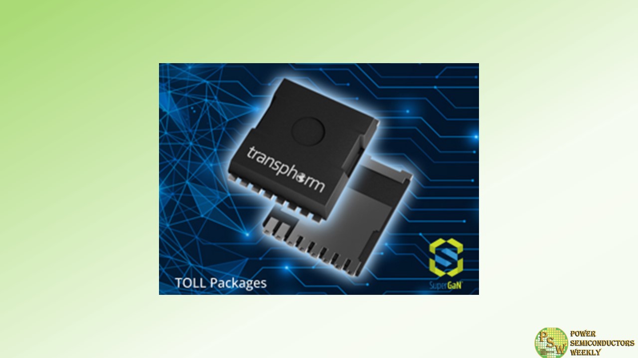
Transphorm, Inc. introduced three SuperGaN® FETs in TOLL packages with on-resistances of 35, 50, and 72 milliohms. Transphorm’s TOLL package configuration is industry standard, meaning the SuperGaN TOLL FETs can be used as drop-in replacements for any e-mode TOLL solution.
The new devices also offer Transphorm’s proven high voltage dynamic (switching) on-resistance reliability that is generally lacking in leading foundry-based e-mode GaN offerings. To sample the devices, visit Transphorm’s product page: https://www.transphormusa.com/en/products/.
The three surface mount devices (SMDs) support higher power applications operating within an average range of 1 to 3 kilowatts. These power systems are typically found in high performance segments such as computing (AI, server, telecom, data center), energy and industrial (PV inverters, servo motors), and other broad industrial markets which, collectively, have a current global GaN TAM of $2.5B. Notably, the FETs are optimal solutions for today’s rapidly expanding AI systems that rely on GPUs requiring 10 to 15 times the power of traditional CPUs.
Transphorm’s high power GaN devices are already widely supplied to leading customers who use them to power in-production high performance systems including datacenter power supplies, high power gaming PSUs, UPSes, and microinverters. These applications can also be supported by the TOLL devices as can electric-vehicle-based DC-to-DC converters and onboard chargers, with the underlying SuperGaN die already automotive (AEC-Q101) qualified.
The SuperGaN TOLL FETs represent the sixth package type offered by Transphorm, giving customers the widest selection of packages to meet their unique design requirements. As with all Transphorm products, the TOLL devices harness the inherent performance and reliability advantages made possible by the normally-off d-mode SuperGaN platform.
For a detailed competitive analysis between SuperGaN and e-mode GaN, download the company’s latest white paper titled The Fundamental Advantages of d-Mode GaN in Cascode Configuration. The white paper’s conclusion aligns with a head-to-head comparison released earlier this year showing the 72 milliohm SuperGaN FETs outperforming larger 50 milliohm e-mode devices in a commercially available 280 W gaming laptop charger.
SuperGaN devices lead the market with unmatched:
- Reliability at < 0.03 FIT
- Gate safety margin at ± 20 V
- Noise immunity at 4 V
- Temperature coefficient of resistance (TCR) at 20% lower than e-mode
- Drive flexibility with standard drivers and protection circuits readily available in silicon-based controllers/drivers
Device Specifications
The robust 650 V SuperGaN TOLL devices are JEDEC qualified. Because the normally-off d-mode platform pairs the GaN HEMT with a low voltage silicon MOSFET, the SuperGaN FETs are easy to drive with commonly used off-the-shelf gate drivers. They can be used in various hard- and soft-switching AC-to-DC, DC-to-DC, and DC-to-AC topologies to increase power density while reducing system size, weight, and overall cost.Part Dimensions (mm) RDS(on) (mΩ) typ RDS(on) (mΩ) max Vth (V) typ Id (25°C) (A) max TP65H035G4QS 10 x 12 35 41 4 46.5 TP65H050G4QS 10 x 12 50 60 4 34 TP65H070G4QS 10 x 12 72 85 4 29 Original – Transphorm
-
Supplier of semiconductor epiwafers, SweGaN, recently began the transformation from start-up to scale-up. AFRY is assisting SweGaN’s scale-up journey with a wide variety of services to build a new state-of-the-art production facility in Linköping. A rapidly growing global sector, semiconductors – are key component within electric vehicles, solar inverters, power supplies and more – all contributing towards a more sustainable society.
AFRY’s cyber security experts are guiding SweGan in securing its IP (Immaterial Properties) and trade secrets and ensuring customer integrity. Additionally, AFRY is providing a bouquet of expert professional services including IT, OT, ERP, CE marking, construction of the new production facility, server room construction, electrical, security, work environment, quality assurance, risk management and project management.
“Initially, we asked AFRY to support and secure our cyber security operations. After understanding AFRY’s wide range of competencies and services, we determined it would be highly favourable to bring all professional services for the new facility under one roof. Partnering with AFRY, we can now focus SweGaN resources on our growth and expansion goals,” says Henrik Tölander, COO SweGaN.
“I am very proud that SweGaN chose us for this project. The client saw the value of one supplier for all their professional service needs. As SweGaN’s full service provider, we can gain a comprehensive, holistic overview of their needs and offer a customer-tailored solution,” says Michael Blom, Section Manager at AFRY.
The opening of the semiconductor production facility will enable Sweden, and in extension Europe, to strengthen the European supply chain and compete against Taiwan, China, the U.S, South Korea and Japan – currently the main providers of semiconductors. Increased access to robust semiconductor offerings in Europe will make it easier to develop and produce electric vehicles, solar inverters, and power supplies in Europe, while also reducing dependency on competing countries.
Original – AFRY
