-

If you haven’t had a chance to visit a wonderful Lake Maggiore yet, this September you can enjoy one of the most beautiful places in Italy in a company of power semiconductors superstars discussing SiC & GaN technologies. After a successful series of events across the world, International Semiconductor Executive Summits (ISES) returns to Italy with ISES EU Power 2023 edition.
With a regional focus on the power semiconductor market, the EU Power International Semiconductor Executive Summits seeks to strengthen the EU supply chain and promote key executives in the semiconductor manufacturing, design, and research through our networking and conference platform which consists of working with key industry stakeholders to encourage progress and collaboration.
With speakers coming from STMicroelectronics, Infineon Technologies, Semikron Danfoss, onsemi, Wolfspeed, Renesas, ROHM, Nexperia, SK Siltron, Soitec, Okmetic, Aehr Test Systems, Amkor Technology, Innoscience, Cambridge GaN Devices, Ferrari, Volkswagen, Volvo, Škoda, and many more leaders of power electronics and automotive industries, you are about to be a part of the power semiconductors event like never before.
During two days of the event, all participants will be discussing and disclosing the latest news and advances in silicon carbide and gallium nitride technologies, sharing the view of the future and taking a close look at the current state of the industry, supply chain, global collaboration, exhisting problems and emerging opportunities.
You can find the agenda of ISES EU Power 2023 at the event website.
International Semiconductor Executive Summit EU Power provides a unique platform for networking and expanding your knowledge base. Here are just a few topics that will be covered this September:
- SiC and GaN Manufacturability
- Variety of WBG Applications
- SiC Wafer & Materials
- Power Packaging
- Design and Reliability
The event offers various packages for participation:
- Standard Pass
- Member Pass
- Partner Pass
- Virtual Pass
- Numerous Sponsorship Packages and VIP Passes
All interested to participate can register at ISES EU Power 2023 website.
ISES EU Power 2023 will take place at Regina Palace Hotel. Overlooking the shore of Lago Maggiore, the Regina Palace Hotel is located in a favored spot in the center of Stresa, considered the pearl of Lago Maggiore. The hotel represents yesteryear’s charm and prestige enriched by the history and the grace that each epoch has donated.
-
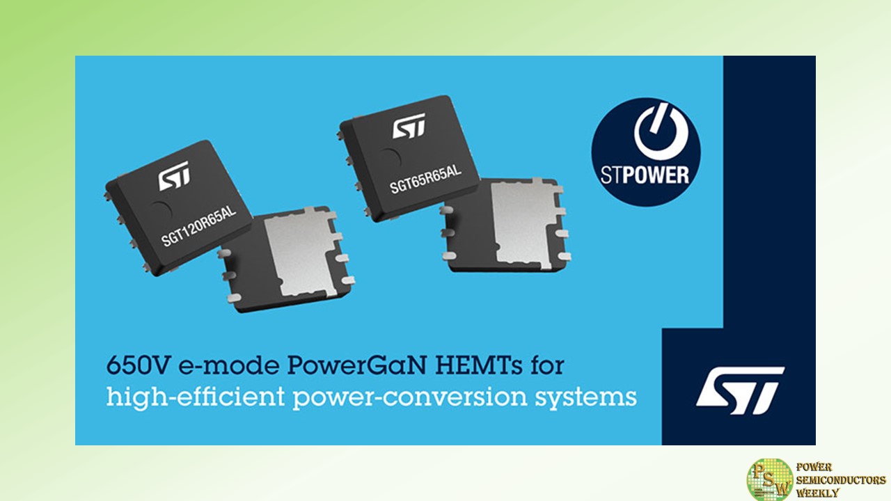
STMicroelectronics has begun volume production of e-mode PowerGaN HEMT (high-electron-mobility transistor) devices that simplify the design of high-efficiency power-conversion systems. The STPOWER™ GaN transistors raise performance in applications such as wall adapters, chargers, lighting systems, industrial power supplies, renewable energy applications, and in automotive electrification.
The first two products in the family, the SGT120R65AL and SGT65R65AL, are industrial-qualified 650V normally-off G-HEMT™ in a PowerFLAT 5×6 HV surface-mount package. They have current ratings of 15A and 25A, respectively, with typical on-resistance (RDS(on)) of 75mΩ and 49mΩ at 25°C.
Also, 3nC and 5.4nC total gate charge and low parasitic capacitances ensure minimal turn-on/turn-off energy losses. A Kelvin source connection allows optimized gate driving. In addition to the reduced size and weight of the power supplies and adapters, the two new GaN transistors provide higher efficiency, lower operating temperature, and extended life time.
In the coming months, ST will introduce new PowerGaN variants, i.e. automotive-qualified devices, as well as additional power-package options including PowerFLAT 8×8 DSC and LFPAK 12×12 for high power applications.
ST’s G-HEMT devices facilitate the transition to GaN wide-bandgap technology in power conversion. GaN transistors with the same breakdown voltage and RDS(on) as silicon alternatives can achieve lower total gate charge and parasitic capacitances, with zero reverse-recovery charge.
These properties raise efficiency and enhance switching performance, allowing higher switching frequency that permits smaller passive components thereby increasing power density. Applications can therefore become smaller with higher performance. In the future, GaN is also expected to enable new power-conversion topologies that will further improve efficiency and decrease power losses.
Original – STMicroelectronics
-
Transphorm, Inc. responded to the recent news regarding China export restrictions. Late Monday, July 3, 2023, China’s Ministry of Commerce stated that it will restrict the exports of materials related to two metals used in semiconductor manufacturing: gallium and germanium. Gallium nitride (GaN) wafer materials are listed as being affected by these regulations.
Transphorm manufactures high voltage GaN power semiconductors. Trimethylgallium (TMGa) is used to produce the GaN. The company confirmed that its primary TMGa suppliers are not based in China and that suppliers have confirmed to be well-positioned to meet forecasted demand. Transphorm is therefore securely positioned to continue manufacturing and supplying its GaN devices without interruption.
Transphorm also explained gallium is generally a byproduct resulting from refinement processes used to produce popular metals such as aluminum from bauxite ore. Aluminum is produced in numerous countries such as Australia, Brazil, India, Jamaica, and the United States among others.
Transphorm will continue to the monitor the situation as necessary but sees no direct impact on its current operations. Nor does the company see long-term sourcing issues.
Original – Transphorm
-
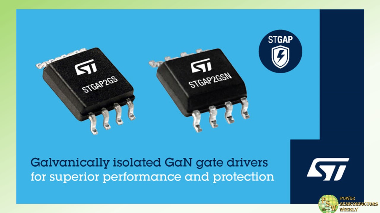
STMicroelectronics’ first galvanically isolated gate driver for gallium-nitride (GaN) transistors, the STGAP2GS, trims dimensions and bill-of-materials costs in applications that demand superior wide-bandgap efficiency with robust safety and electrical protection.
The single-channel driver can be connected to a high-voltage rail up to 1200V, or 1700V with the STGAP2GSN narrow-body version, and provides gate-driving voltage up to 15V. Capable of sinking and sourcing up to 3A gate current to the connected GaN transistor, the driver ensures tightly controlled switching transitions up to high operating frequencies.
With minimal propagation delay across the isolation barrier, at just 45ns, the STGAP2GS ensures fast dynamic response. In addition, dV/dt transient immunity of ±100V/ns over the full temperature range guards against unwanted transistor gate change. The STGAP2GS is available with separate sink and source pins for easy tuning of the gate-driving operation and performance.
Saving the need for discrete components to provide optical isolation, the STGAP2GS driver eases the adoption of efficient and robust GaN technology in various consumer and industrial applications. These include power supplies in computer servers, factory-automation equipment, motor drivers, solar and wind power systems, home appliances, domestic fans, and wireless chargers.
In addition to integrating galvanic isolation, the driver also features built-in system protection including thermal shutdown and under-voltage lockout (UVLO) optimized for GaN technology, to ensure reliability and ruggedness.
Two demonstration boards, the EVSTGAP2GS and EVSTGAP2GSN, combine the standard STGAP2GS and narrow STGAP2GSN with ST’s SGT120R65AL 75mΩ, 650V enhancement-Mode GaN transistors to help users evaluate the drivers’ capabilities.
The STGAP2GS in SO-8 widebody package, and the STGAP2GSN SO-8 narrow version, are available now, priced from $1.42 for orders of 1000 pieces.
Please visit www.st.com/stgap2gs for more information.
Original – STMicroelectronics
-

Navitas Semiconductor has confirmed continued supply of leading-edge gallium nitride (GaN) power ICs. On July 3rd, 2023, China’s Ministry of Commerce announced it would put in place certain restrictions on the exporting of gallium and germanium, among other materials, starting in August. Navitas’ wafer technology is ‘GaN-on-Si’. The wafer subcontract manufacturer has verified that their production remains unaffected by the export restrictions, given multiple sources of gallium world-wide.
As a result, Navitas does not expect customer deliveries to be impacted or its business to be adversely affected by the export restrictions.
Significant sources of gallium are available worldwide, as it is a natural by-product in the production of other metals such as aluminum. Navitas does not use germanium in any product.
Original – Navitas Semiconductor
-

Kulicke and Soffa Industries, Inc. announced the launch of several new systems and capabilities serving high-volume semiconductor and fast-growing power-semiconductor applications.
POWERCOMM™ and POWERNEXX™ represent the next evolution in advanced wire bonding systems and are designed with a new generation of intuitive advanced process capabilities which deliver maximum levels of performance, efficiency, and productivity. Additionally, both systems deliver enhanced mean time between assists (MTBA), with automated recovery features that improve the machine to operator ratio and better support localization of semiconductor assembly.
The POWERCOMM™ advanced wire bonding solution is designed to support high-volume discrete and low-pin count devices commonly used in applications such as data centers, automotive, industrial automation, smartphones, wearables and connected devices.
The POWERNEXX™ advanced wire bonding solution is optimized for higher density QFN packages with widths of up to 100mm. The improved illumination design on POWERNEXX™ allows faster alignment time through its Pattern Recognition System (PRS). Faster alignment and advanced process capabilities deliver the industry leading UPH and lowest Cost-of-Ownership.
In addition to the new POWERCOMM™ and POWERNEXX™ systems, K&S extends its leadership in wedge bond applications with new High-Power-Interconnect (HPI) capabilities addressing the emerging needs of power devices. HPI capabilities are becoming increasingly necessary to assemble applications such as inverters, battery assembly and charging infrastructure which support the growth and increasing efficiency requirements of sustainable energy and electric vehicle applications. The need for more efficient and higher-current applications are driving rapid changes to the power semiconductor market by increasing demand in emerging compound semiconductors, such as Silicon Carbide (SiC) and Gallium Nitride (GaN), but are also demanding new capabilities to support next-generation battery assembly and are accelerating the transition from aluminum wire and ribbon, to copper wire and ribbon. Next generation HPI capabilities are being introduced across Kulicke & Soffa’s leading wedge bonder portfolio today.
“Our rich history of innovation and ongoing development priorities are enabling us to provide additional value to the increasingly critical assembly process. This recent set of new wire bonding systems and capabilities will better enable customers to optimize productivity, improve material handling capabilities and significantly lower cost-of-ownership,” said Shawn Sarbacker, Kulicke and Soffa’s Vice President of Ball Bonder Business Unit.
Original – Kulicke and Soffa Industries
-

Nidec Corporation and Renesas Electronics Corporation have agreed to join forces on the development of semiconductor solutions for a next-generation E-Axle (X-in-1 system) that integrates an EV drive motor and power electronics for electric vehicles (EVs).
Today’s EVs are increasingly adopting the 3-in-1 unit called E-Axle, which integrates a motor, inverter, and gearbox (reduction gear). To realize high-performance and efficiency as well as smaller size, light weight and lower cost, and to accelerate vehicle development, EVs are also integrating power electronics controls such as DC-DC converters and on-board chargers (OBCs). EV manufacturers in advanced markets such as China have developed an X-in-1 platform that integrates multiple functions, accelerating the adoption in many vehicle models.
As X-in-1 integrates multiple functions and increases in complexity, maintaining a high-level of quality in vehicles becomes challenging. Thus, developing preventive safety technologies such as diagnostic functions and failure prediction is crucial for ensuring safety and security in vehicles. To address this challenge, the two companies agreed to combine Nidec’s motor technology and Renesas’ semiconductor technology to jointly develop a highly reliable and high-performance proof of concept (PoC) for the X-in-1 system. The PoC is designed to support the industry’s highest performance and efficiency as well as smaller size, light weight and lower cost for the X-in-1 system.
The companies plan to launch the first PoC by the end of 2023, which will feature a 6-in-1 system with a DC-DC converter, OBC, and power distribution unit (PDU) as well as a motor, inverter, and gearbox. As a second phase in 2024, Nidec and Renesas plan to develop a highly integrated X-in-1 PoC that incorporates a battery management system (BMS) along with other components. The first PoC will include power devices based on SiC (silicon carbide), and the second PoC will replace the DC-DC and OBC power devices with GaN (gallium nitride), offering excellent performance in high-frequency operation, to further reduce size and cost.
Building on the PoC developed through this collaboration, Nidec plans to rapidly productize E-Axle systems to add to its portfolio and ramp up to mass production to lead the E-Axle market. Renesas plans to develop and deliver turnkey solutions for increasingly complex X-in-1 systems by expanding the jointly developed PoC for E-Axle reference designs.
Original – Renesas Electronics
-

AIXTRON SE plans to invest up to 100 million euros at its Herzogenrath site. A new innovation center is to be built, which will provide the manufacturer of deposition equipment to the semiconductor industry with enhanced capacities for research and development. AIXTRON received approval for the new project from the company’s Supervisory Board.
The new innovation center will provide 1000m2 of cleanroom space and will be built on the company’s premises in Herzogenrath, Germany. The new building will create further capacities for the next product generations which are already in preparation, as well as for further product developments beyond that.
“With our products, we address the megatrends of digitalization, electromobility and energy efficiency and are experiencing a strong and steadily growing demand. Technical innovations and product developments that precisely address the needs of our customers are the key to our success. And our dynamic environment offers us further growth opportunities,” says Dr. Felix Grawert, CEO of AIXTRON SE. “We are therefore very pleased that the Supervisory Board has approved this project which will enable us to create the foundation for further product developments and for future growth.”
The importance of product development in the dynamic semiconductor industry is demonstrated by the success of AIXTRON’s new “G10” system generations. In the first year after market introduction, AIXTRON expects to generate more than 40 percent of its annual revenues with this new product generation. Right after its official launch, the new tool for the silicon carbide material system (G10-SiC) has already generated a high order intake. And it is expected to continue to drive further growth all throughout 2023 and beyond.
Also, the new AIXTRON solution for the gallium-arsenide/indium-phosphite material system (G10-AsP) which was launched at the beginning of 2023 already enjoys a strong demand. For the first time, it enables the high-volume production of Micro LEDs and photonic components such as lasers on wafers with a diameter of up to 200mm. Later in the year, the new G10 system for gallium nitride (GaN) will also be launched. The material systems SiC and GaN have the potential to fully cover the complete range of power electronics, from electromobility to renewable energy technologies to fast data transmission. With their outstanding material properties, they will ensure a significant reduction in global CO2 emissions in these areas and help electromobility achieve a breakthrough.
Original – AIXTRON
-
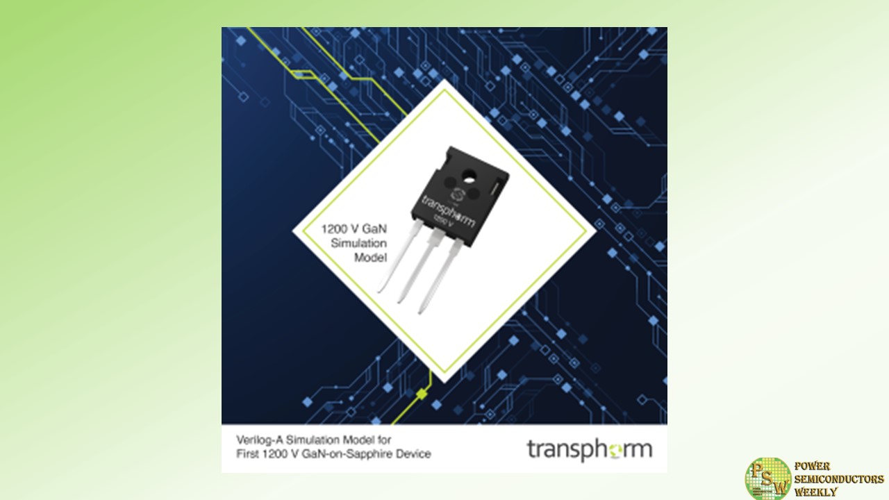
Transphorm, Inc. announced availability of its 1200 V FET simulation model and preliminary datasheet. The TP120H070WS FET is the only 1200 V GaN-on-Sapphire power semiconductor introduced to date, making its model the first of its kind. Its release indicates Transphorm’s ability to support future automotive power systems as well as three-phase power systems typically used in the broad industrial, datacom, and renewables markets. These applications will benefit from the 1200 V GaN device’s higher power density and reliability along with equal or better performance at more reasonable cost points versus alternative technologies.
Transphorm recently validated the GaN device’s higher performance ability in a 5 kW 900 V buck converter switching at 100 kHz. The 1200 V GaN device achieved 98.7% efficiency, exceeding that of a similarly rated production SiC MOSFET.
The innovative 1200 V technology also underscores Transphorm’s leadership in GaN power conversion. Vertical integration, epitaxy ownership, and patented process paired with decades of engineering expertise enable the company to bring to market the highest performing GaN device portfolio with four additional major differentiators: Manufacturability, Drivability, Designability, and Reliability.
Transphorm’s 1200 V technology is anchored in proven process and mature technology, satisfying customer confidence requirements. The GaN-on-Sapphire process is in volume production today in the LED market. Additionally, the 1200 V technology leverages the fundamentally superior, normally-off GaN platform used in Transphorm’s current device portfolio.
Key TP120H070WS device specifications include:
- 70 mΩ RDS(on)
- Normally off
- Efficient bidirectional current flow
- ± 20 Vmax gate robustness
- Low 4Vth gate drive noise immunity
- Zero QRR
- 3-lead TO-247 package
The Verilog-A device model is recommended for use with the SIMetrix Pro v8.5 Circuit Simulator. A LTSpice model is in development and will be released in Q4 2023. Simulation modeling allows for fast and efficient power system design validation while reducing design iterations, development time, and hardware investments.
The device model files and datasheet are available for download here: https://www.transphormusa.com/en/products/#models
1200 V FET samples are expected to be available by Q1 2024.
Original – Transphorm
-
Power electronics technologies have undergone a radical transformation following the introduction of wide-bandgap (WBG) devices, such as silicon carbide (SiC) and gallium nitride (GaN). These materials, in fact, have characteristics that make them particularly suitable for applications that operate at high voltages and high switching frequencies. To fully exploit the potential offered by wide-bandgap semiconductors, designers must understand the challenges of these materials.
Power electronics design will continue to focus on reducing the size and complexity of devices while increasing their functionality. The design will increasingly incorporate AI and machine learning algorithms to improve performance, monitor system health, and optimize energy management. Future developments will be integrated not only in automotive, industrial, aerospace markets, but also with IoT technologies to create a more connected and automated energy system.
Semiconductor devices are used to drive motors and control power. As efficiency standards for these applications get better, cost-effective and energy-efficient control solutions, test and measurement solutions, and transducers/sensors make design easier and offer a high level of integration, as well as better safety features and certified isolation capabilities.
Moreover, using energy harvesting techniques and new power semiconductors to make electrical and electronic systems work as well as possible is an important part of engineering.
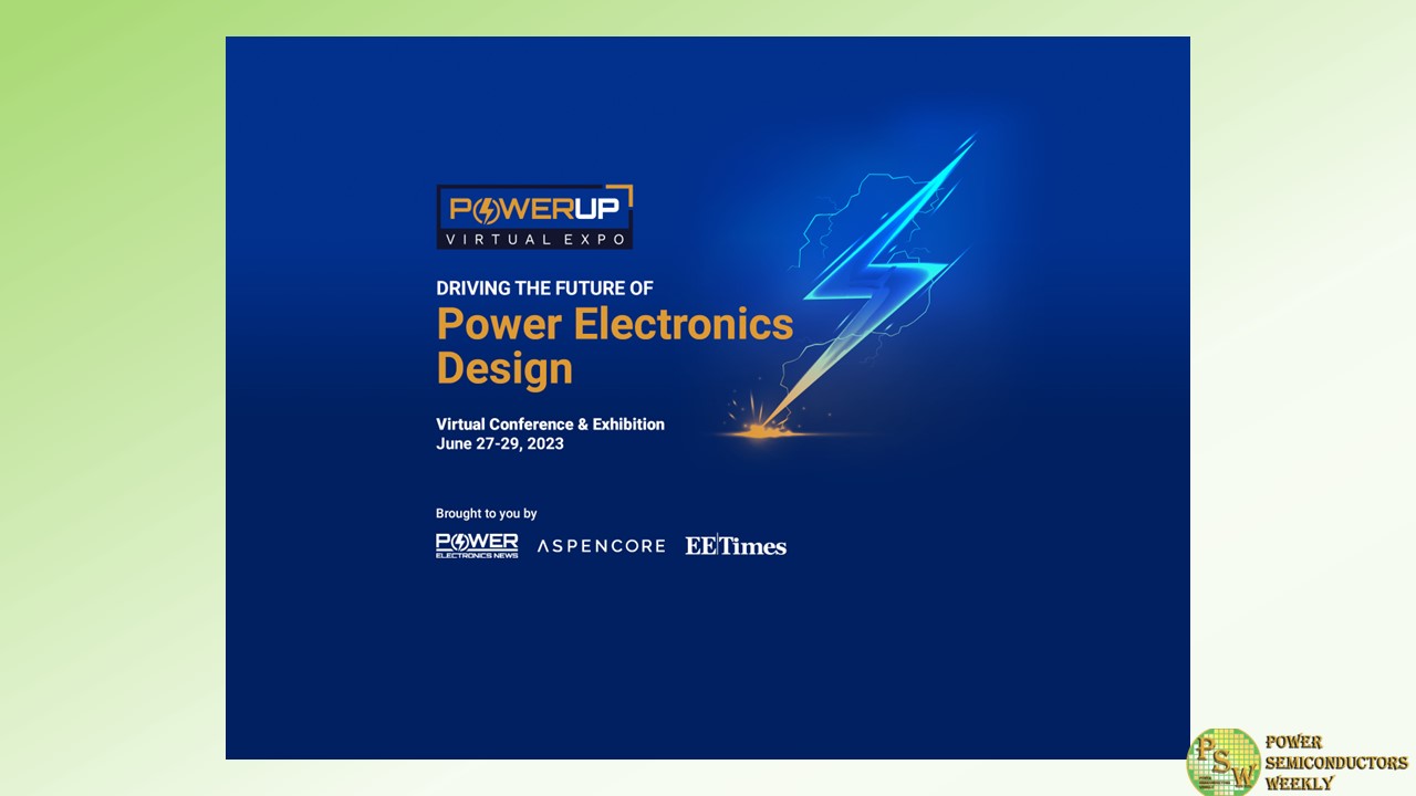
The PowerUP Expo is a three-day virtual conference and exhibition focusing on power electronics. With an exhibition area, live stage, and messaging center, the PowerUP Expo functions similarly to a live exhibition and conference. This technical conference will include a number of sessions including keynotes, panel discussions, technical presentations, and tutorials on a variety of subject matters, including significant technical trends, market demands, and new application areas. The exhibition area will include virtual booths from top power electronics businesses and a Live Chat facility that allows attendees to communicate with booth staff directly.
PowerUP offers an opportunity for engineers, managers, academics, and students from all over the world to learn the latest technological advances and applications in Power Electronics and to connect with each other in our community. The newest trends and advancements in the field of power electronics, from components to intelligent systems, are discussed by leaders in the industry.
Conference Tracks:
- June 27: Tutorial/Lectures, Panel Discussion & Conference Preview
- June 28: Wide Bandgap Semiconductors and Power Applications
- June 29: Power Conversion and Management Design Trends in low and high power
Detailed agenda can be found at PowerUP Expo.
Original – PowerUP Expo
