-

Navitas Semiconductor is set to unveil a breakthrough in power conversion that will create a paradigm shift across multiple major end markets. These developments include both semiconductor and system innovations which are expected to drive major improvements in energy efficiency & power density and further accelerate the adoption of gallium nitride and silicon carbide technologies to displace silicon.
The live-streamed event will take place on March 12th at 8 am PST and will be re-streamed (in both Chinese and English) at 6 pm PST.
Co-founders, Gene Sheridan (CEO), Dan Kinzer (CTO, COO) and Jason Zhang (VP Engineering) will uncover this next inflection in power conversion, including technology details, specific application examples and describe the expected market impacts & business opportunities from these innovations.
- Register now, 8 am Pacific: https://bit.ly/NavitasLiveEvent-8am-PT
- Register now, 6 pm Pacific: https://bit.ly/NavitasLiveEvent-6pm-PT
Original – Navitas Semiconductor
-

Efficient Power Conversion Corporation (EPC) announced the release of the 4th edition of its groundbreaking textbook, GaN Power Devices for Efficient Power Conversion.
This latest edition reflects the rapid advancements in GaN technology and its transformative impact across various industries, including renewable energy, electric vehicles, data centers, robotics, and space applications. Co-authored by EPC CEO Dr. Alex Lidow and a team of GaN experts, the textbook remains an indispensable resource for engineers, students, and industry innovators looking to stay at the forefront of power electronics.
What’s New in the 4th Edition
- Expanded coverage on the integration of GaN into new applications such as AI servers, autonomous systems, and eMobility
- Updates on design techniques that maximize GaN’s superior efficiency, power density, and thermal performance
- Comprehensive insights into GaN ICs and their role in simplifying complex designs and improving system reliability
- A dedicated section on the latest advancements in GaN reliability and manufacturability
- Real-world application examples, case studies, and practical design tips for engineers.
“Since its inception, this textbook has guided engineers and innovators adopting GaN,” said Dr. Alex Lidow, CEO and co-author. “The 4th edition deepens understanding of GaN’s capabilities and empowers readers to unlock its full potential.”
This edition underscores EPC’s commitment to educating the power electronics community and supporting the adoption of GaN as the go-to technology for efficient power conversion. The textbook is available for purchase through Wiley.
Availability and Additional Resources
The 4th edition of GaN Power Devices for Efficient Power Conversion is available now. For additional resources, including evaluation boards, design support tools, and application notes, visit epc-co.com.
Original – Efficient Power Conversion
-

Navitas Semiconductor’s 8.5kW power supply unit (PSU), powered by GaNFast™ and GeneSiC™ technologies, has been recognized for its innovative design. Tailored for AI and hyperscale data centers, the PSU achieves 98% efficiency while meeting Open Compute Project (OCP) and Open Rack v3 (ORv3) specifications.
The design minimizes ripple current, EMI, and device count by 25%, reducing costs. Its 3-phase LLC topology utilizes GaNSafe™ technology with integrated control, drive, sensing, and protection, along with Gen-3 Fast SiC MOSFETs for enhanced performance and reliability.
Original – Navitas Semiconductor
-

Navitas Semiconductor announced its adoption of both technologies into Dell’s family of notebook adapters, from 60 W to 360 W.
Enabled by over 20 years of SiC technology leadership, GeneSiC leads on performance of SiC MOSFETs with patented ‘trench-assisted planar’ technology and 5th-gen GeneSiC silicon carbide (SiC) diodes to deliver high-speed, high-efficiency performance with proprietary ’low-knee’ technology for cool operation.
Navitas’ GaNFast power ICs enable high-frequency, high-efficiency power conversion, achieving 3x more power and 3x faster charging in half the size and weight compared to prior designs with legacy silicon power devices.
Navitas GaN & SiC technology together enables Dell to provide high-speed charging, with highest efficiency, coolest temperature, smallest size, and lowest material count. Dell’s latest line-up of AI notebooks includes Neural Processor Units (NPUs), which are dedicated AI engines, to manage sustained AI and AI offload. This builds on Dell’s portfolio as the broadest GaN adapter offering for notebooks in the industry.
The new adapters will also help Dell achieve its advanced sustainability goals, with a focus on CO2 reduction and energy reduction. The adapter cases require up to 50% less plastic and are made with post-recycled materials, significantly reducing energy waste, and improving resource utilization. Navitas’ GaNFast and GeneSiC technologies increase the level of system integration and switching frequency, which reduces the number of components, as well as the size, resulting in a ‘dematerialization’ that lowers carbon footprint throughout the production, packaging, and logistics processes. Each GaNFast power IC shipped saves 4 kg CO2 and every SiC MOSFET shipped saves 25 kg CO2 vs. legacy silicon power chips.
“Since Dell’s first GaN adapter was enabled by Navitas back in 2020, we’ve worked closely with Dell engineering to further improve charging speed, efficiency, size, weight, and now environmental footprint”, said Gene Sheridan, CEO and co-founder of Navitas. “Dell’s new adapters are an optimal solution for speed, portability, and sustainability. Our clients achieve a win-win for both the market and environment by deploying Navitas GaNFast power ICs and GeneSiC power devices.”
Original – Navitas Semiconductor
-

As the world continues to face the challenges of climate change and environmental sustainability, Infineon Technologies AG is at the forefront of innovation, harnessing the power of all relevant semiconductor materials including silicon (Si), silicon carbide (SiC), and gallium nitride (GaN) to drive meaningful progress towards decarbonization and digitalization.
In its 2025 predictions – GaN power semiconductors, Infineon highlights that gallium nitride will be a game-changing semiconductor material revolutionizing the way we approach energy efficiency and decarbonization across consumer, mobility, residential solar, telecommunication, and AI data center industries. GaN provides significant benefits in end customers’ applications enabling efficient performance, smaller size, lighter weight, and lower overall cost. While USB-C chargers and adapters have been the forerunners, GaN is now on its way to reaching tipping points in its adoption in further industries, substantially driving the market for GaN-based power semiconductors.
”Infineon is committed to driving decarbonization and digitalization through innovation based on all semiconductor materials Si, SiC, and GaN,” said Johannes Schoiswohl, Head of the GaN Business Line at Infineon. “The relevance of comprehensive power systems will increase with GaN manifesting its role due to its benefits in efficiency, density, and size. Given that cost-parity with silicon is in sight, we will see an increased adoption rate for GaN this year and beyond.
Powering AI will be highly depending on GaN. The rapid increase of required computing power and energy demand in AI data centers will drive the need for advanced solutions capable of handling the substantial loads associated with AI servers. Power supplies that once managed 3.3 kW are now evolving towards 5.5 kW, with projections moving towards 12 kW or more per unit. By leveraging GaN, AI data centers can improve power density, which directly influences the amount of computational power that can be delivered within a given rack space. While GaN presents clear advantages, hybrid approaches combining GaN with Si and SiC are ideal for meeting the requirements of AI data centers and achieving the best trade-offs between efficiency, power density and system cost.
In the home appliance market, Infineon expects GaN to gain significant traction, driven by the need for higher energy efficiency ratings in applications like washing machines, dryers, refrigerators and water/heat pumps. In 800 W applications, for example, GaN can enable a two percent efficiency gain, which can help manufacturers achieve the coveted A ratings. According to Infineon, GaN-based on-board chargers and DC-DC converters in electric vehicles will contribute to a higher charging efficiency, power density, and material sustainability, with a shift towards 20 kW+ systems. Together with high-end SiC solutions, GaN will also enable more efficient traction inverters for both 400 V and 800 V EV systems, contributing to an increased driving range.
In 2025 and beyond, robotics will see widespread adoption of GaN supported by the material’s ability to enhance compactness, driving growth in delivery drones, care robots and humanoid robots. As robotics technology integrates AI advancements like natural language processing and computer vision, GaN will provide the efficiency required for compact, high-performance designs. Integrating inverters within the motor chassis eliminates the inverter heatsink while reducing cabling to each joint/axis and simplifying EMC design.
Infineon is further pushing investment in GaN research and development to overcome the challenges of cost and scalability. With the broadest product and IP portfolio, the highest quality standards, leading-edge innovations such as 300 mm GaN wafer manufacturing and bidirectional switch (BDS) transistors, the company is bolstering its leading role in driving decarbonization and digitalization based on all relevant semiconductor materials including gallium nitride.
Download the “2025 GaN predictions” ebook here.
Original – Infineon Technologies
-

Efficient Power Conversion Corporation (EPC) announced the launch of the EPC91104, a high-performance 3-phase BLDC motor drive inverter reference design. This innovative design is ideal for powering compact, precision motors in humanoid robots, such as those used for wrist, finger, and toe movements.
The EPC91104 evaluation board uses the EPC23104 ePower™ Stage IC, offering a maximum RDS(on) of 11 mΩ and supporting DC bus voltages up to 80 V. The design supports up to 14 Apk steady-state and 20 Apk pulsed current, ensuring reliable performance for humanoid robot applications that require fine motor control and precision.
Key Features of the EPC91104
- Wide Voltage Range: Operates between 14 V and 80 V, accommodating a variety of battery systems
- Compact Design: Suitable for space-constrained robotics
- Advanced Protection: Includes overcurrent and input undervoltage protection, ensuring reliability in demanding applications
- Optimized Efficiency: Low-distortion switching reduces torque ripple and motor noise
Humanoid robots demand motors with precision and compactness, and the EPC91104 is specifically designed to meet those needs for applications like small joint actuation,
said Alex Lidow, CEO of EPCFor higher-current requirements, such as elbow and knee motors in humanoid robots, EPC offers the EPC9176 board in the same family. With enhanced current capacity, the EPC9176 complements the EPC91104 to cover a full range of motor drive applications in humanoid robotics.
The EPC91104 is compatible with controller boards from leading manufacturers, including Microchip, Texas Instruments, STMicroelectronics, and Renesas, offering engineers flexibility in development. It is equipped with comprehensive sensing and protection features, ensuring rapid prototyping and testing.
Original – Efficient Power Conversion
-

Toyoda Gosei’s technology to enhance GaN substrates has been verified to improve power device performance. An article confirming it was published in Physica Status Solidi (RRL) – Rapid Research Letters, an international scientific journal for solid state physics.
Better power devices are indispensable for CO2 reduction in society, as they regulate electric power everywhere. Switching material from silicon to gallium nitride enables 90% energy-saving, superior devices, for which mass production of larger quality GaN substrates is requisite.
The Japanese Ministry of the Environment is leading a project for broad application of GaN power devices, for which Toyoda Gosei is providing technology to obtain ideal GaN crystals. One outcome of the project is a demonstrable improvement in power device performance with a GaN substrate fabricated on a GaN seed crystal that Toyoda Gosei jointly developed with Osaka University. Compared to power devices made on commercially-available substrates, power devices using these GaN substrates show higher performance in both power regulation capacity and yield ratio.
Toyoda Gosei will continue collaborating with government, universities, and other corporations for earlier dissemination of large quality GaN substrates.
Original – Toyoda Gosei
-

Aehr Test Systems has received an initial production order from a top tier automotive semiconductor supplier for a FOX-XP™ wafer level test and burn-in system with fully integrated FOX WaferPak™ Aligner for production test of their gallium nitride (GaN) power semiconductor devices. The FOX-XP system with integrated WaferPak Aligner is scheduled to ship immediately.
Gayn Erickson, President and CEO of Aehr Test Systems, commented, “We have been working closely with this customer for over a year to support their evaluation and qualification process for delivering GaN power semiconductor devices to their customers. We are thrilled to receive this initial production purchase order, signaling their commitment to move forward with volume production wafer level burn-in of their GaN devices on our FOX-XP platform.
“This customer has extensively utilized a FOX-NP system under an evaluation agreement for production qualification and reliability testing of their devices over the past year. As part of the evaluation, they purchased a significant number of our proprietary WaferPak full wafer Contactors to successfully qualify a wide range of GaN device types designed for multiple end use applications including industrial, solar, data center, and automotive markets.
“Our FOX-P platform allows customers using the FOX-NP for device qualification and reliability testing of power semiconductors like GaN and silicon carbide (SiC) to transition seamlessly to the FOX-XP multi-wafer fully automated system, which is capable of testing up to nine wafers in parallel and is specifically designed to handle high-voltage testing and high temperature Gate and Drain stress test requirements. By leveraging our FOX-XP system and our proprietary WaferPak full wafer Contactors, customers can easily test wafers of varying sizes from 6 to 12 inches by simply purchasing new WaferPaks, while utilizing the same FOX-XP system and FOX WaferPak Aligner.
“Like SiC, GaN semiconductor MOSFETs are wide bandgap devices that offer significantly higher power conversion efficiency than silicon. GaN is particularly well suited for lower power applications such as sub-1000-watt power converters (fast chargers) used in consumer electronics like cell phones, tablets, and laptops. Additionally, it is increasingly being adopted for automotive power converters, supporting electrical systems in both electric and traditional gasoline-powered cars, as well as being targeted at data center power applications where power efficiency and delivery are critical to support the massive amount of computing power and data storage being installed over the next decade. Along with the increased usage in automotive and data centers, many industry experts and analysts predict that GaN MOSFETs will eventually replace silicon as the preferred technology for power conversion in photovoltaic (solar panel) applications.
“We view GaN as a transformative and rapidly growing technology in the power semiconductor market. With an anticipated compound annual growth rate of more than 40%, the GaN market is projected to reach $2.5 billion in annual device sales by 2029 according to Yole Group’s Power SiC/GaN Compound Semiconductor Market Monitor. In addition, Frost & Sullivan estimates GaN semiconductors will account for over 10% of the worldwide power semiconductor industry by the year 2028. This represents a significant growth opportunity for Aehr’s wafer level test and burn-in solutions.”
The FOX-XP and FOX-NP systems, available with multiple WaferPak Contactors (full wafer test) or multiple DiePakTM Carriers (singulated die/module test) configurations, are capable of functional test and burn-in/cycling of devices such as silicon carbide and gallium nitride power semiconductors, artificial intelligence processors, silicon photonics as well as other optical devices, 2D and 3D sensors, flash memories, magnetic sensors, microcontrollers, and other leading-edge ICs in either wafer form factor, before they are assembled into single or multi-die stacked packages, or in singulated die or module form factor.
Original – Aehr Test Systems
-
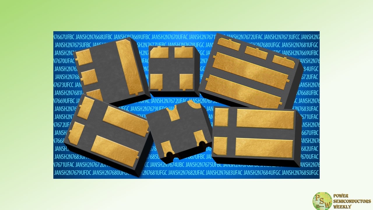
EPC Space announced that both its Andover, Massachusetts facility and its wafer fabrication facility in Taiwan have been certified under the JANS MIL-PRF-19500 standard.
This certification marks a significant milestone, highlighting EPC Space’s commitment to excellence and its role as a leader in providing top-tier semiconductor solutions for critical space applications. The MIL-PRF-19500 certification, managed by the U.S. Department of Defense, sets the bar for reliability, performance, and environmental resilience in semiconductor components. EPC Space’s achievement in obtaining this certification for Gallium Nitride (GaN) High Electron Mobility Transistors (HEMT) is a world first.
Bel Lazar, CEO of EPC Space, commented, “Securing the JANS certification is a direct result of our relentless pursuit of quality. Our teams have worked tirelessly to ensure our products not only meet but exceed the expectations for reliability in the most demanding conditions.”
Alex Lidow, CEO of EPC Corporation, commented, “that the commitment to the MIL-PRF-19500 standard not only guarantees the durability and performance of EPC Space’s products but also reinforces the company’s dedication to supporting its customers in achieving their critical objectives.”
Looking ahead, EPC Space is set to launch 18 JANS certified Rad Hard GaN HEMT parts, ranging from 40V to 300V, throughout 2025. This expansion will further solidify EPC Space’s role as a key supplier of high-reliability electronics, crucial for space missions and other high-stakes applications.
Original – EPC Space
-

ROHM and TSMC have entered a strategic partnership on development and volume production of gallium nitride (GaN) power devices for electric vehicle applications.
The partnership will integrate ROHM’s device development technology with TSMC’s industry-leading GaN-on-silicon process technology to meet the growing demand for superior high-voltage and high-frequency properties over silicon for power devices.
GaN power devices are currently used in consumer and industrial applications such as AC adapters and server power supplies. TSMC, a leader in sustainability and green manufacturing, supports GaN technology for its potential environmental benefits in automotive applications, such as on-board chargers and inverters for electric vehicles (EVs).
The partnership builds on ROHM and TSMC’s history of collaboration in GaN power devices. In 2023, ROHM adopted TSMC’s 650V GaN high-electron mobility transistors (HEMT), whose process is increasingly being used in consumer and industrial devices as part of ROHM’s EcoGaN™ series, including the 45W AC adapter (fast charger) “C4 Duo” produced by Innergie, a brand of Delta Electronics, Inc.
“GaN devices, capable of high-frequency operation, are highly anticipated for their contribution to miniaturization and energy savings, which can help achieve a decarbonized society. Reliable partners are crucial for implementing these innovations in society, and we are pleased to collaborate with TSMC, which possesses world-leading advanced manufacturing technology” said Katsumi Azuma, Member of the Board and Senior Managing Executive Officer at ROHM. “In addition to this partnership, by providing user-friendly GaN solutions that include control ICs to maximize GaN performance, we aim to promote the adoption of GaN in the automotive industry.”
“As we move forward with the next generations of our GaN process technology, TSMC and ROHM are extending our partnership to the development and production of GaN power devices for automotive applications,” said Chien-Hsin Lee, Senior Director of Specialty Technology Business Development at TSMC. “By combining TSMC’s expertise in semiconductor manufacturing with ROHM’s proficiency in power device design, we strive to push the boundaries of GaN technology and its implementation for EVs.”
Original – ROHM
