-

VisIC Technologies announced a new partnership aimed at advancing high-efficiency GaN inverter technology for the EV market. This collaboration will provide automotive OEMs with power semiconductors that exceed silicon carbide (SiC) performance, while offering lower costs at device and system level.
In a recent test conducted at AVL’s state-of-the-art facilities in Germany, an inverter based on VisIC’s GaN-on-Silicon D³GaN components proved an outstanding performance. Mounted on AVL’s e-motor test bench and controlled by AVLs SOP eDrive controls algorithm, the system achieved a benchmark efficiency level of 99.67% at 10kHz, stunningly climbing to over 99.8% efficiency at 5kHz — which outperforms comparable SiC inverters by up to 0.5% and is cutting energy losses by more than 60%.
This breakthrough positions the AVL and VisIC partnership as a compelling option for automakers striving to balance high efficiency with affordability in EV design. It is worth noting that VisIC’s GaN-on-Silicon power devices require significantly less energy and therefore CO2 during the chip production process compared to SiC. They can be produced in widespread 200mm and 300mm silicon foundries, which makes scaling production a straightforward process.
“With AVL, we’re making cutting-edge GaN inverter technology accessible for even more electric vehicles, establishing a new benchmark for efficiency and cost-effectiveness in the industry,” said Gregory Bunin, CTO of VisIC Technologies. “Our partnership reflects a shared commitment to driving EV innovation that’s both impactful and accessible, bringing GaN’s unparalleled performance to a broader market.”
“Working with VisICs new GaN power module for high-power systems enables us to offer our customers cutting-edge solutions that are optimally aligned with the requirements of next-generation drive systems. These include, among other things, high power density combined with reduced overall system costs,” added Dr. Thomas Frey, Head of Segment E-Mobility & E-Drive System at AVL Software and Functions GmbH. “Together, we can significantly advance e-mobility and help reduce the carbon footprint.”
Looking ahead, AVL and VisIC plan to expand their GaN-on-Si platform to include 800V GaN power modules, ensuring that their technology remains scalable and adaptable to the needs of the growing BEV market. This collaboration places AVL and VisIC Technologies at the forefront of GaN inverter technology, establishing new standards for energy efficiency and performance across the EV industry.
Original – VisIC Technologies
-

GlobalFoundries has received an additional $9.5 million in federal funding from the U.S. government to advance the manufacturing of GF’s essential gallium nitride (GaN) on silicon semiconductors at its facility in Essex Junction, Vermont.
The funding moves GF closer to large-scale production of GaN chips. With the ability to handle high voltages and temperatures, GaN chip technology is essential for enabling higher performance and greater energy efficiency across a range of RF and high-power control applications including automobiles, datacenter, IoT, aerospace and defense.
With the award, GF will continue to add new tools, equipment and prototyping capabilities to its market-leading GaN IP portfolio and reliability testing as the company moves closer to full-scale manufacturing of its 200mm GaN chips in Vermont. GF is committed to creating a fast and efficient path for customers to realize new innovative designs and products that leverage the unique efficiency and power management benefits of GaN chip technology.
“GF is proud of its leadership in GaN chip technology, which is positioned to make game-changing advances across multiple end-markets and enable new generations of devices with more energy-efficient RF performance and faster-charging, longer-lasting batteries,” said Nicholas Sergeant, vice president of IoT and aerospace and defense at GF. “We appreciate the U.S. government’s partnership and ongoing support of our GaN program. Realizing full-scale GaN chip manufacturing will be a catalyst for innovation, for both our commercial and government partners, and will add resilience and strengthen the semiconductor supply chain.”
The new funding, awarded by the U.S. Department of Defense’s Trusted Access Program Office (TAPO), represents the latest federal investment to support GF’s GaN program in Vermont.
“This strategic investment in critical technologies strengthens our domestic ecosystem and national security, and ensures these assets are readily available and secure for DoD utilization. In concert with key partners, this approach fortifies defense systems, empowering resilience and responsiveness,” said Dr. Nicholas Martin, Director at Defense Microelectronics Activity.
In total, including the new award, GF has received more than $80 million since 2020 from the U.S. government to support research, development and advancements to pave the way to full-scale GaN chip manufacturing.
Vermont is a U.S.-accredited Trusted Foundry and the global hub of GF’s GaN program, with longstanding leadership in 200mm semiconductor manufacturing. In July 2024, GF acquired Tagore Technology’s Gallium Nitride Power portfolio and created the GF Kolkata Power Center in Kolkata, India. The center is closely aligned with and supports GF’s facility in Vermont, and is helping advance GF’s research, development and leadership in GaN chip manufacturing.
Original – GlobalFoundries
-

Cambridge GaN Devices (CGD) and IFP Energies nouvelles (IFPEN), a major French public research and training organization in the fields of energy, transport and the environment, have developed a demo which confirms the suitability of CGD’s ICeGaN®650 V GaN ICs in a multi-level, 800 VDC inverter.
The demo delivers super-high power density – 30 kW/l – which is greater than can be achieved by more expensive, state-of-the-art silicon-carbide (SiC)-based devices. The inverter realization also demonstrates the ease of paralleling that ICeGaN technology enables; each inverter node has three 25mΩ / 650V ICeGaN ICs – 36 devices in total – in parallel.
ANDREA BRICCONI | CHIEF MARKETING OFFICER, CGD
“We are super excited at this first result of our partnership with IFPEN. 800 VDC supports the 800 V bus which is being increasingly adopted by the EV industry. By addressing automotive and other high voltage inverter applications with energy-efficient ICeGaN-based solutions we are delivering on CGD’s key commitment – sustainability.”This multi-level GaN Inverters can power electric motors to over 100 kW peak, 75 kW continuous power. The CGD/IFPEN demo features: a high voltage input of up to 800Vdc; 3-phase output; a peak current of 125 Arms (10s) (180 Apk); and a continuous current of 85 Arms continuous (120 Apk).
The ICeGaN multi-level design proposed by IFPEN reveals several compelling benefits:
- Increased Efficiency: the improvement in the efficiency of the traction inverter leads to an increase in battery range and a reduction in charging cycles. It also leads to a reduction in battery cost if the initial range (iso-range) is maintained
- Higher switching frequencies: GaN transistors can operate at much higher frequencies than silicon transistors. This reduces iron losses in the motor, particularly in the case of machines with low inductances
- Reduced Electromagnetic Interferences: 3-level topology minimizes EMI and enhances the reliability of the system
- Enhanced thermal management: insulated metallized substrate boards featuring an aluminium core facilitate superior thermal dissipation, ensuring optimal operating temperatures and extending the lifespan of the system and associated GaN devices
- Modular design: this facilitates scalability and adaptability for varying system requirements.
GAETANO DE PAOLA | PROGRAM MANAGER, IFPEN
“Following the implementation of this inverter reference using CGD’s enabling ICeGaN ICs coupled with innovative topologies, such as multi-level solutions, IFPEN now strongly believes that GaN is a breakthrough technology in terms of performance and cost for high-voltage traction inverters.”Original – Cambridge GaN Devices
-

Cambridge GaN Devices (CGD) and Qorvo® have partnered to bring together industry-leading motor control and power efficiency technologies in the PAC5556A + ICeGaN® evaluation kit (EVK). This collaboration combines Qorvo’s high-performance BLDC/PMSM motor controller/driver and CGD’s easy-to-use ICeGaN ICs in a board that significantly improves motor control applications.
ANDREA BRICCONI | CHIEF MARKETING OFFICER, CGD
“By combining industry-leading solutions from our two technology-strong companies in this EVK, we are enabling the development of compact, energy-efficient systems with high power density. Unlike other GaN implementations, ICeGaN technology easily interfaces with Qorvo’s PAC5556A motor control IC for seamless high performance in BLDC and PMSM applications.”JEFF STRANG | GENERAL MANAGER, POWER MANAGEMENT BUSINESS UNIT, QORVO
“Wide-bandgap semiconductors like GaN and SiC are being integrated into motor control applications for the power density and efficiency advantages they offer. CGD’s ICeGaN technology delivers ease of use and reliability – two critical factors for motor control and drive designers. Customers are responding enthusiastically when they experience the power of GaN combined with our highly integrated PAC5556A 600V BLDC motor control solution.”By employing CGD’s latest-generation P2 ICs, the PAC5556AEVK2 evaluation kit with 240 mΩ ICeGaN achieves up to 400W peak performance without a heatsink, whilst the PAC5556AEVK3 with 55 mΩ ICeGaN hits 800W peak with minimal airflow cooling.
ICeGaN’s efficiency gains result in reduced power loss, increased power availability, and minimized heat dissipation, enabling smaller and more reliable systems. Because ICeGaN integrates essential current sense and Miller clamp elements, gate driver design is simplified and BOM costs are reduced. This makes the solution easy to implement and price-competitive, as well as high performance.
The PAC5556A + CGD GaN EVKs offer higher torque at low speeds and precise control, making them ideal for white goods, ceiling fans, refrigerators, compressors and pumps. Target markets include industrial and home automation, especially where compact, high-efficiency motor control systems are required. PAC5556AEVK2 and PAC5556AEVK3 are now available to order at Qorvo’s website.
Original – Cambridge GaN Devices
-

Efficient Power Conversion (EPC) announced that the Full Commission of the U.S. International Trade Commission (ITC) has affirmed the ITC’s initial determination that Innoscience infringed EPC’s foundational patent for GaN technology, which is core to applications involving artificial intelligence, satellites, rapid chargers, humanoid robots, and autonomous driving, among others. The decision imposes a ban on Innoscience (Zhuhai) Technology Co., Ltd. and its affiliates (Innoscience) from importing GaN-related products into the United States without a license from EPC.
This milestone decision marks the first successfully litigated U.S. patent dispute involving GaN-based wide bandgap semiconductors and solidifies EPC’s position as a leading developer of these next-generation devices, which are significantly more efficient, faster, and smaller than traditional, silicon-based technology. The decision also paves the way for EPC to expand access to its IP through licensing agreements with potential partners and customers around the world.
“After pouring nearly two decades and immense resources into developing our uniquely valuable intellectual property portfolio, this is a tremendous victory for EPC and a major win for fair competition globally, which is critical to the success of next-generation technological advances. We are grateful to the ITC for their diligent work in recognizing the validity of our patents and Innoscience’s infringement,” said Alex Lidow, CEO and Co-Founder of EPC. “EPC will continue to vigorously defend our IP against unfair use to ensure that we can continue to innovate and provide our customers with the cutting-edge technologies needed to help power our future.”
The ITC’s most recent decision is the fourth time that EPC’s IP rights have been affirmed against Innoscience in the past six months. EPC initially filed the infringement claim against Innoscience in the ITC in May 2023. In response, Innoscience challenged the validity of the EPC patents at issue in the U.S., as well as EPC’s counterpart patents in China.
The China National Intellectual Property Administration upheld the validity of EPC’s counterpart patents in April and May 2024. The ITC’s initial determination in July 2024 similarly confirmed the validity of the challenged patents, and also found that Innoscience infringed EPC’s foundational patent, U.S. Patent No. 8,350,294. The ITC’s final determination is subject to a 60-day Presidential review period, expiring on January 6, 2025.
Original – Efficient Power Conversion
-

Navitas Semiconductor has announced the world’s first 8.5 kW power supply unit (PSU), powered by GaN and SiC technologies to achieve 98% efficiency, for next-generation AI and hyperscale data centers.
The AI-optimized 54V output PSU complies with Open Compute Project (OCP) and Open Rack v3 (ORv3) specifications and utilizes high-power GaNSafe and Gen-3 Fast SiC MOSFETs configured in 3-phase interleaved PFC and LLC topologies, to ensure the highest efficiency and performance, with lowest component count. The PSU’s shift to a 3-phase topology for both the PFC and LLC (vs. 2-phase topologies used by competing PSUs) enables the industry’s lowest ripple current and EMI.
Furthermore, the PSU reduces the number of GaN and SiC devices by 25% compared with the nearest competing system, which reduces the overall cost. The PSU has an input voltage range of 180 to 264 Vac, a standby output voltage of 12 V, and an operating temperature range of -5oC to 45oC. Its hold-up time at 8.5 kW is 10 ms, with 20 ms possible through an extender.
The 3-Phase LLC topology is enabled by high-power GaNSafe, which is specifically created for demanding, high-power applications, such as AI data centers and industrial markets. Navitas’ 4th generation integrates control, drive, sensing, and critical protection features that enable unprecedented reliability and robustness. GaNSafe is the world’s safest GaN with short-circuit protection (350ns max latency), 2kV ESD protection on all pins, elimination of negative gate drive, and programmable slew rate control. All these features are controlled with 4-pins, allowing the package to be treated like a discrete GaN FET, requiring no VCC pin. Suitable for applications from 1 kW to 22 kW, 650 V GaNSafe in TOLL and TOLT packages are available with a range of RDS(ON)MAX from 25 to 98 mΩ.
The 3-Phase interleaved CCM TP-PFC is powered by Gen-3 Fast SiC MOSFETs with ‘trench-assisted planar’ technology, which has been enabled by over 20 years of SiC innovation leadership and offers world-leading performance over temperature, delivering cool-running, fast-switching, and superior robustness to support faster charging EVs and up to 3x more powerful AI data centers.
“This complete wide bandgap solution of GaN and SiC enables the continuation of Navitas’ AI power roadmap which enables this 8.5kW and plans to drive to 12kW & higher in the near-term”, said Gene Sheridan, CEO and co-founder of Navitas. “As many as 95% of the world’s data centers cannot support the power demands of servers running NVIDIA’s latest Blackwell GPUs, highlighting a readiness gap in the ecosystem. This PSU design directly addresses these challenges for AI and hyperscale data centers.”
The PSU will be on display for the first time at Electronica 2024 (Hall C 3, booth 129, November 12th– 15th).
Original – Navitas Semiconductor
-

EPC Space announced the launch of HEMTKY product line.
A HEMTKY is a HEMT, High Electron Mobility Transistor, with an embedded Schottky diode. The presence of an antiparallel Schottky diode in the HEMTKY structure minimizes third quadrant conduction losses absent GaN HEMT synchronous drive. Notable advantages are:
- Predictable conduction losses, no reverse recovery charge
- Reduced system sensitivity to half-bridge deadtime variance
- Reduced negative voltage stress on gate drivers
For 500-unit quantities, engineering models are priced at $212 USD each, while space level units are priced at $315 USD each.
EPC Space provides revolutionary high-reliability radiation-hardened enhancement-mode gallium nitride power management solutions for space and other harsh environments. Radiation hardened GaN-based power devices address critical spaceborne environments for applications such as power supplies, motor drives, ion thrusters, and more. eGaN is a registered trademark of Efficient Power Conversion Corporation, Inc.
Original – EPC Space
-

Cambridge GaN Devices (CGD) will exhibit at Electronica which runs from November 12-15, 2024 at the Messe München, Munich, Germany. This will be the second time that the company has exhibited at the world’s leading trade fair and conference for electronics, marking the company’s position as a leader in delivering gallium-nitride power ICs which are easy to use and very reliable.
ANDREA BRICCONI | CHIEF MARKETING OFFICER, CGD
“Since our first appearance at Electronica, CGD has made remarkable steps. We have introduced our P2 series ICeGaN® ICs that feature RDS(on) levels down to 25 mΩ, supporting multi kW power levels with the highest efficiency. We have announced a deal with TSMC, the leading IC fabrication house in the world which ensures quality and supply of our innovative power devices. Also, studies by leading academic research establishment, Virginia Tech University, have demonstrated that our ICeGaN GaN technology is more reliable and robust than other GaN platforms. GaN is now available for use at higher power levels, and at Electronica we are expecting to meet with designers who are eager to take advantage of the efficiency and power density benefits that GaN can bring to their latest designs.”During the show, CGD will make two presentations:
- November 12, 13:20 – 14:10, Booth A5.351: SiC & GaN Technologies – Exploring Advancements, Addressing Challenges CGD’s CTO and co-founder, Professor Florin Udrea will join a panel of GaN experts for a Panel Discussion moderated by Maurizio Di Paolo Emilio, Editor-in-Chief, Power Electronics News.
- November 12, 16:10-16:35, Power Electronics Forum: ICeGaN as a smart high voltage platform for high power industrial and automotive applications presented by Professor Florin Udrea.
The power devices field has undergone significant change due to the emergence of Wide Band Gap semiconductors, particularly Gallium Nitride (GaN) and Silicon Carbide (SiC). Traditionally, GaN has been used for lower power consumer applications (e.g., power supplies), while SiC dominated the medium to high power markets, such as industrial (e.g., motor drives) and automotive applications (e.g., traction inverters).
SiC’s superior scaling of on-state resistance at high voltages gives it an edge above 1.2 kV, but GaN is now competing with SiC at 650V for all power levels. ICeGaN®, featuring sensing and protection functions, surpasses discrete SiC in terms of robustness and ease of paralleling, offering notable advantages for 650V high-power applications. Additionally, with the rise of multi-level topologies for traction inverters, GaN may challenge SiC’s 1.2 kV market. Ultimately, both technologies have a bright future, with overlap expected in high-power (10-500 kW) applications.
At Electronica, CGD will show a number of demos that employ ICeGaN, including:
- 3 kW totem-pole PFC evaluation board;
- High and low power QORVO motor drive evaluation kits developed in collaboration with CGD and utilising ICeGaN
- Half-bridge and full-bridge evaluation boards, plus an ICeGaN in parallel evaluation board;
- Single leg of a 3-phase 800 V automotive inverter demo board, developed in partnership with French public R&I institute, IFP Energies nouvelles (IFPEN);
- ICeGaN vs discrete GaN circuits comparison in half bridge (daughter cards) demo board.
- High-density USB-PD adaptor developed with Industrial Technology Research Institute (ITRI) of Taiwan
Original – Cambridge GaN Devices
-

Infineon Technologies AG announced the launch of a new family of high-voltage discretes, the CoolGaN™ Transistors 650 V G5, further strengthening its Gallium Nitride (GaN) portfolio. Target applications for this new product family range from consumer and industrial switched-mode power supply (SMPS) such as USB-C adapters and chargers, lighting, TV, data center and telecom rectifiers to renewable energy and motor drives in home appliances.
The latest CoolGaN generation is designed as a drop-in replacement for the CoolGaN Transistors 600 V G1, enabling rapid redesign of existing platforms. The new devices provide improved figures of merit to ensure competitive switching performance in focus applications.
Compared to key competitors and previous product families from Infineon, the CoolGaN Transistors 650 V G5 offer up to 50 percent lower energy stored in the output capacitance (E oss), up to 60 percent improved drain-source charge (Q oss) and up to 60 percent lower gate charge (Q g). Combined, these features result in excellent efficiencies in both hard- and soft-switching applications. This leads to a significant reduction in power loss compared to traditional silicon technology, ranging from 20 to 60 percent depending on the specific use case.
These benefits allow the devices to operate at high frequencies with minimal power loss, resulting in superior power density. The CoolGaN Transitors 650 V G5 enable SMPS applications to be smaller and lighter or to increase the output power range in a given form factor.
The new high-voltage transistor product family offers a wide range of R DS(on) package combinations. Ten R DS(on) classes are available in various SMD packages, such as ThinPAK 5×6, DFN 8×8 , TOLL and TOLT. All products are manufactured on high-performance 8-inch production lines in Villach (Austria) and Kulim (Malaysia). In the future, CoolGaN will transition to 12-inch production. This will enable Infineon to further expand its CoolGaN capacity and ensure a robust supply chain in the GaN power market, which is expected to reach $2 billion by 2029, according to Yole Group.
A demo featuring the CoolGaN Transistors 650 V G5 will be showcased at electronica 2024 in Munich from November 12 to 15 (hall C3, booth 502).
Original – Infineon Technologies
-
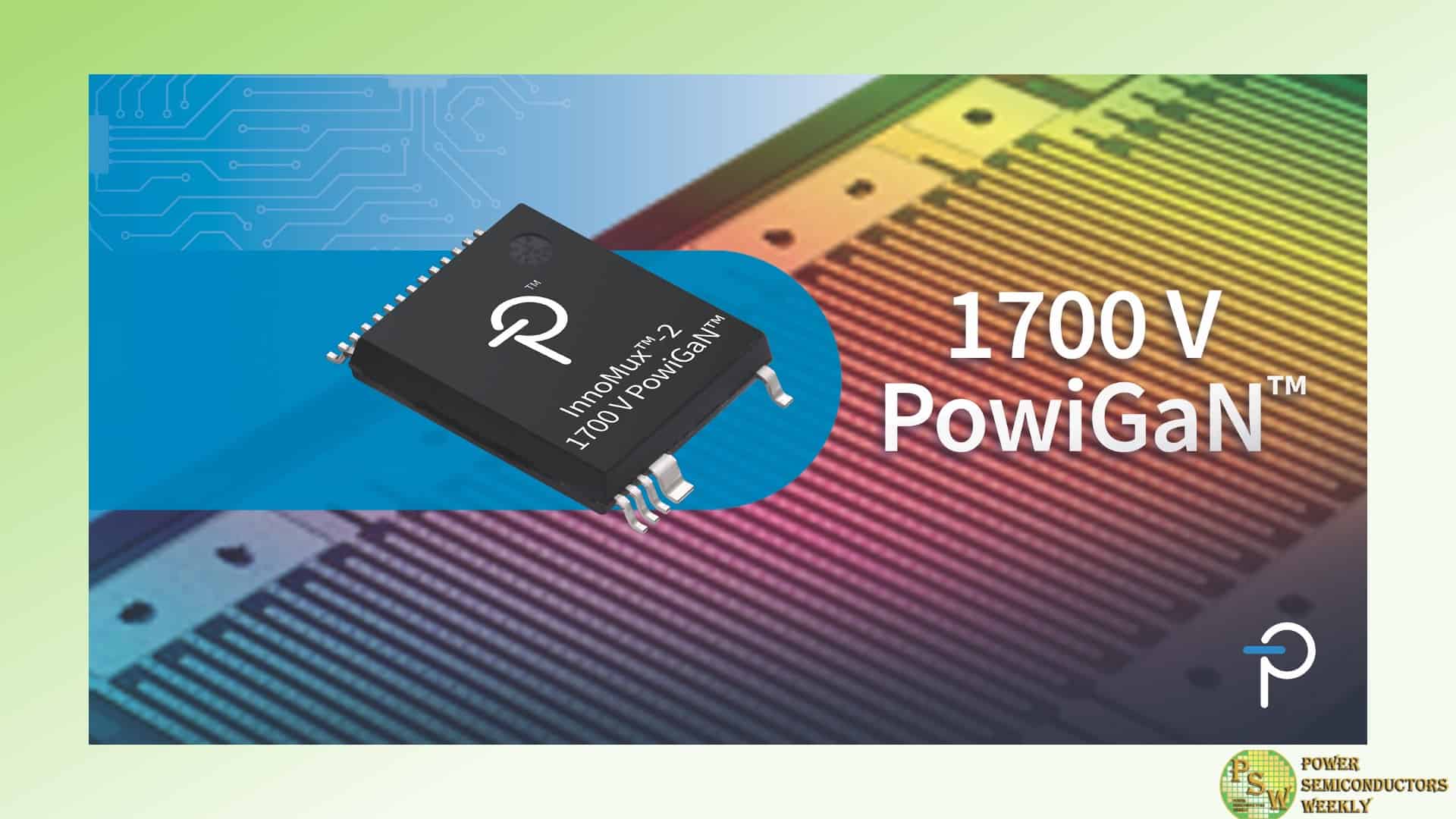
Power Integrations introduced a new member of its InnoMux™-2 family of single-stage, independently regulated multi-output offline power supply ICs. The new device features the industry’s first 1700 V gallium nitride switch, fabricated using the company’s proprietary PowiGaN™ technology.
The 1700 V rating further advances the state-of-the-art for GaN power devices, previously set by Power Integrations’ own 900 V and 1250 V devices, both launched in 2023. The 1700 V InnoMux-2 IC easily supports 1000 VDC nominal input voltage in a flyback configuration and achieves over 90 percent efficiency in applications requiring one, two or three supply voltages.
Each output is regulated within one percent accuracy, eliminating post regulators and further improving system efficiency by approximately ten percent. The new device replaces expensive silicon carbide (SiC) transistors in power supply applications such as automotive chargers, solar inverters, three-phase meters and a wide variety of industrial power systems.
Radu Barsan, vice president of technology at Power Integrations, said, “Our rapid pace of GaN development has delivered three world-first voltage ratings in a span of less than two years: 900 V, 1250 V and now 1700 V. Our new InnoMux-2 ICs combine 1700 V GaN and three other recent innovations: independent, accurate, multi-output regulation; FluxLink™, our secondary-side regulation (SSR) digital isolation communications technology; and zero voltage switching (ZVS) without an active-clamp, which all but eliminates switching losses.”
Original – Power Integrations
