-

SweGaN AB, a European semiconductor manufacturer that develops and produces custom engineered Gallium Nitride on Silicon Carbide (GaN-on-SiC) epitaxial wafers, reported orders for its benchmark QuanFINE® epiwafers worth 17 MSEK in the first half of 2024, including three large frame agreements from undisclosed major Telecom and Defense market players. The company reported a 100% YoY order increase and began deliveries from its new facility in Linköping, Sweden, marking significant progress in its scale-up journey.
In additional notable news, the semiconductor manufacturer announces a newly completed QuanFINE epiwafer customer qualification with a device manufacturer.
In the last two years, SweGaN has displayed an exciting operational transformation in alignment with its growth strategy and global demands for GaN-on-SiC epiwafers. Securing a Series A investment round, the company has scaled its organization, established a streamlined team, and deployed a new high-capacity production facility to drive its growth strategy and future KPIs.
– “Today we celebrate three significant milestones that signal SweGaN’s transition from a pure R&D company to a rigorous global semiconductor manufacturer.” says Dr. Jr-Tai Chen, CEO at SweGaN.
– “Currently, there is a strong momentum in the Telecom industry to upgrade technology from 5G to 5G Advanced, continues Chen. SweGaN’s patented QuanFINE® buffer-free GaN-on-SiC material is well-suited to meet the demanding technical requirements of the new technology, particularly in terms of device efficiency and thermal management. This applies to the new Telecom standard 5G Advanced, as well as the strong demands for enhanced sensing capability in Defense applications. The new framework orders will accelerate product development and production ramp-up enabling SweGaN to tap the market opportunities in both the Telecom and Defense sectors.”
With SweGaN’s new production facility in full swing, the company has the tools to fully embrace its ambitious scale-up strategy and significantly boost manufacturing capacity of next-generation GaN-on-SiC engineered epitaxial wafers. Simultaneously, the company aims to continue to innovate through new R&D initiatives and deepen partnerships with suppliers and customers to establish resilient supply chains.
– “I take immense pride in our synergistic team, in both successfully qualifying SweGaN’s first epiwafer product with a device manufacturer and executing on the significant undertaking of bringing the the new high-capacity wafer production facility into operation, from planning to deployment,” continues Chen.
Original – SweGaN
-
DCDC converters are essential in any electric or hybrid vehicle to connect the high-voltage battery to the low-voltage auxiliary circuits. This includes 12 V power headlights, interior lights, wiper and window motors, fans, and at 48 V, pumps, steering drives, lighting systems, electrical heaters, and air conditioning compressors. In addition, the DCDC converter is important for developing more affordable and energy-efficient vehicles with an increasing number of low voltage functions.
According to TechInsights, the global automotive DC-DC converter market size was valued at USD 4 billion in 2023 and is projected to grow to USD 11 billion by 2030, exhibiting a CAGR of 15 percent during the forecast period. Gallium nitride (GaN) in particular plays a crucial role here, as it can be used to improve the power density in DCDC converters and on-board chargers (OBC).
For this reason, Vitesco Technologies, a leading supplier of modern drive technologies and electrification solutions, has selected GaN to improve the power efficiency of its Gen5+ GaN Air DCDC converter. The CoolGaN™ Transistors 650 V from Infineon Technologies AG significantly improve the overall system performance while minimizing system cost and increasing ease of use. As a result, Vitesco created a new generation of DCDC converters that set new standards in power density (efficiency of over 96%) and sustainability for power grids, power supplies, and OBCs.
The advantages of GaN-based transistors in high-frequency switching applications are considerable, but even more important is the high switching speed, which has been increased from 100 kHz to over 250 kHz. This enables very low switching losses, even in hard-switched half-bridges, with minimized thermal and overall system losses.
In addition, Infineon’s CoolGaN Transistors feature high turn-on and turn-off speeds and are housed in a top-cooled TOLT package. They are air-cooled, eliminating the need for liquid cooling and thereby reducing overall system costs. The 650 V devices also improve power efficiency and density, enabling an output of 800 V. In addition, they feature an ON-resistance (R DS(on)) of 50 mΩ, a transient drain-to-source voltage of 850 V, an I DS,max of 30 A, and an I DSmax,pulse of 60 A.
“We are delighted to see industry leaders like Vitesco Technologies using our GaN devices and innovating with their applications,” said Johannes Schoiswohl, Senior Vice President & General Manager, GaN Systems Business Line Head at Infineon. “The ultimate value of GaN is demonstrated when it changes paradigms, as in this example of moving from a liquid-cooled system to an air-cooled system.”
With GaN Transistors, Vitesco Technologies was able to design its Gen5+ GaN Air DCDC converters with passive cooling, which reduces the system’s overall cost. The GaN devices also allow for simplified converter design and mechanical integration. As a result, the DCDC converters can be flexibly positioned in the vehicle, reducing the workload for manufacturers.
The use of GaN also allows the power of the converters to be scaled up to 3.6 kW and the power density to be increased to over 4.2 kW/l. The Gen5+ GaN Air DCDC converters offer an efficiency of over 96 percent and improved thermal behavior compared to the Gen5 Liquid-Cooled converters. They provide a two-phase output of 248 A at 14.5 V continuous.
The phases can be combined to achieve the maximum output power. Still, it is also possible to switch off one phase under partial load conditions and interleave the switching frequency between the two phases. In addition, by switching the input of two phases in series, the converters based on the CoolGaN power transistors 650 V can be used to implement 800 V architectures without exceeding the maximum blocking voltage of the device. The converters also feature an isolated half-bridge topology consisting of a GaN-based half-bridge, a fully isolated transformer, and an active rectifier unit for each phase.
Original – Infineon Technologies
-

Navitas Semiconductor announced that Samsung had expanded adoption of Navitas’ GaNFast ICs from the original flagship Galaxy S22, S23 and S24 to the mainstream Galaxy A, and revolutionary Galaxy Z Fold6 and Galaxy Z Flip6 smartphones with enhanced Galaxy AI features.
GaN runs up to 20x faster than legacy silicon and enables chargers up to 3x more power and 3x faster charging in half size and weight. GaNFast power ICs enable high-frequency, high-efficiency power conversion, achieving up to a 50% shrink vs. prior designs.
The new 25W charger (EP-T2510) features new energy-saving technology to reduce standby losses by 75% to only 5 mW, which aligns with Navitas’ environmental advances, where every GaNFast IC saves 4 kg of CO2 vs. legacy silicon chips.
“Since enabling the world’s first production GaN charger in 2018, Navitas has pioneered and leads the adoption of GaN to replace legacy silicon chips,” noted David Carroll, Sr. VP Worldwide Sales for Navitas. “Our production partnership with Samsung dates back to the Galaxy S22 Ultra, and today’s announcement reflects the dramatic expansion of GaN from niche, flagship designs to adoption in high-volume, mainstream phones.”
Original – Navitas Semiconductor
-
Many different trends are taking center stage in both consumer electronics and industrial applications, such as portability, electrification, and weight reduction. All of these trends require compact and efficient designs. They also go hand in hand with unconventional PCB designs with severe space constraints that limit the use of external components.
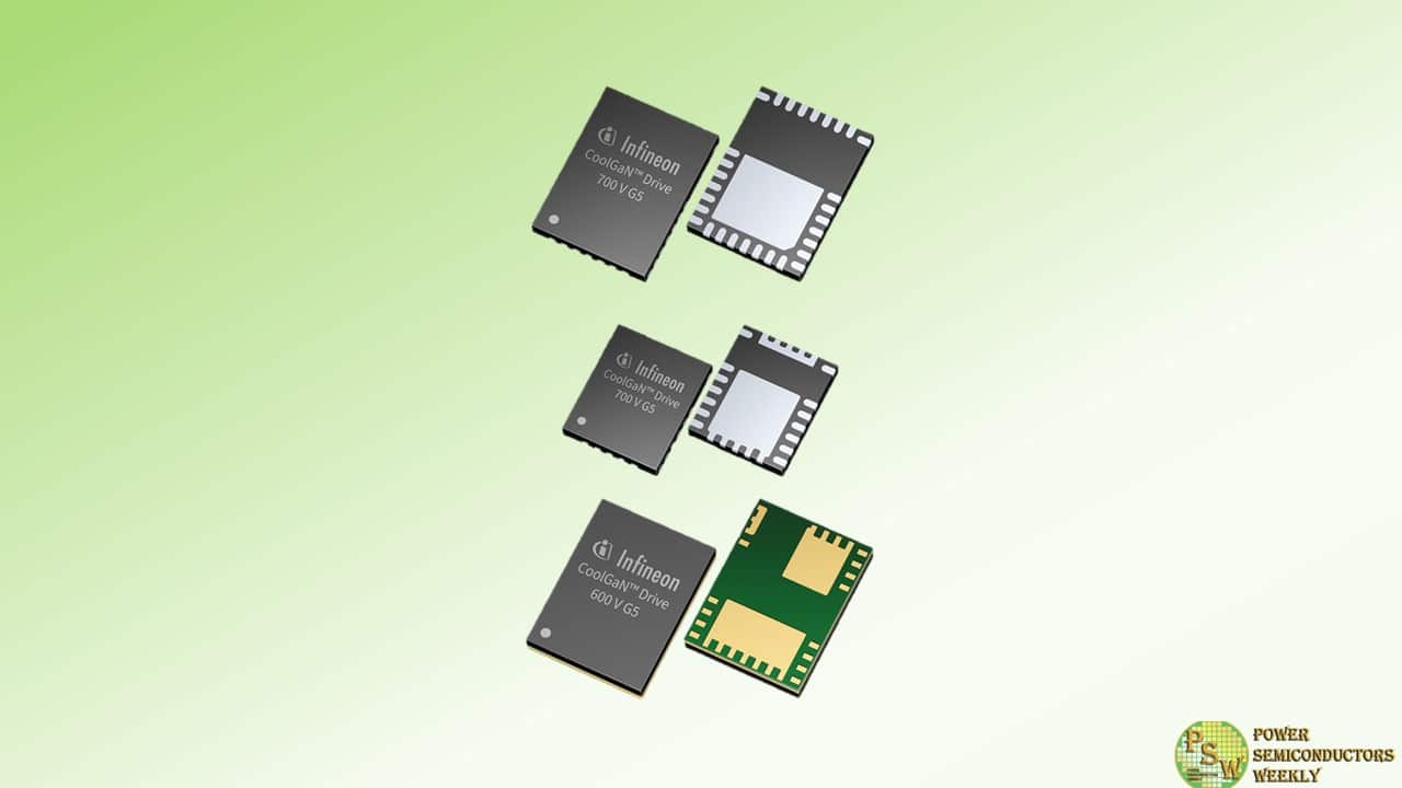
To address these challenges, Infineon Technologies AG expands its GaN portfolio with the CoolGaN™ Drive product family. It consists of the CoolGaN Drive 700 V G5 single switches, integrating one transistor plus gate driver in PQFN 5×6 and PQFN 6×8 packages, as well as the CoolGaN Drive HB 600 V G5 devices, combining two transistors with integrated high- and low-side gate drivers in a LGA 6×8 package. The new product family enables improved efficiency, reduced system size, and overall cost savings. This makes the devices suitable for longer-range e-bikes, portable power tools, and lighter-weight household appliances such as vacuums, fans, and hairdryers.
“For several years, Infineon has been focused on accelerating innovation in GaN to provide targeted solutions for real-world power challenges”, said Johannes Schoiswohl, Senior Vice President & General Manager, GaN Systems Business Line Head at Infineon. “The new CoolGaN Drive product family is another proof point of how we support our customers in developing compact designs with high power density and efficiency through GaN.”
The CoolGaN Drive family offers a wide range of single switches and half bridges with integrated drivers based on the recently announced CoolGaN Transistors 650 V G5. Depending on the product group, the components feature a bootstrap diode and are characterized by loss-free current measurement, and adjustable switch-on and switch-off dV/dt. They also provide OCP/OTP/SCP protection functions. As a result, the devices enable higher switching frequencies, leading to smaller and more efficient system solutions with high power density. At the same time, the bill of materials (BoM) is reduced. This not only results in a lower system weight, but also reduces the carbon footprint.
Samples of the half-bridge solutions are available now. Single-switch samples will be available starting Q4 2024. Further information is available at www.infineon.com/GaN-innovations.
Original – Infineon Technologies
-

VisIC Technologies Ltd. has partnered with Heraeus Electronics and PINK to develop an advanced power module utilizing D3GaN technology. This groundbreaking power module is based on a silicon nitride (Si₃N₄) ceramic substrate, an innovative silver (Ag) sintering process and advanced top side interconnect, promising unprecedented reliability and performance for battery electric vehicles (BEVs).
The collaboration brings together VisIC’s expertise in GaN-based devices, Heraeus Electronics’ cutting-edge packaging materials know-how, and PINK’s state-of-the-art sintering technology. The synergy of these industry leaders has culminated in the development of a power module that is setting new standards for GaN based power modules to revolutionize the EV industry.
VisIC’s D3GaN technology is at the heart of this power module, offering significant improvements in efficiency, thermal management, and power density. This technology leverages the superior electrical properties of gallium nitride to deliver faster switching speeds and higher power handling capabilities compared to traditional silicon-based devices.
The use of a Si₃N₄ metal ceramic substrate is a key innovation in this power module. Si₃N₄ is known for its excellent thermal conductivity, mechanical strength, and reliability under high-temperature conditions. These properties are crucial for the demanding environment of electric vehicle applications, ensuring the power module can withstand the rigors of everyday use while maintaining optimal performance.
The adoption of the silver sintering process by PINK enhances the thermal and electrical conductivity of the module. Silver sintering is a low-temperature bonding process that creates robust and reliable connections between components, improving the module’s overall durability and efficiency. This process is critical for the high reliability required in EV powertrains, where consistent performance is non-negotiable.
The resulting power module is designed to meet the stringent reliability and performance standards of the electric vehicle industry. Its advanced materials and innovative construction techniques ensure it can deliver the high-power density of over 500Arms/650V and efficiency needed for modern BEVs, while also offering long-term reliability and durability at a cost point near silicon devices.
This collaboration marks a significant milestone in the advancement of power electronics for electric vehicles. The integration of VisIC’s D3GaN technology with Heraeus Electronics’ sintering paste and PINK’s Ag and Cu sintering process and flexible sintering equipment sets a new benchmark for power module performance in the EV market. This innovation is expected to drive the adoption of GaN technology in EV applications, paving the way for more efficient, reliable, and sustainable electric transportation solutions.
Tamara Baksht, CEO of VisIC, state: “We are thrilled to work with the leading manufacturer of sintering processes of Heraeus Electronics and PINK and adapt their experience into GaN based power modules to develop the next generation of power module for high volume automotive inverter applications.”
PINK, Andrea Pink, CEO of PINK statement: “We are excited to work with such a future driven company as VisIC together with our long-term partner Heraeus Electronics, supporting the newest product innovation for GaN applications.”
Heraeus Electronics Dr. Michael Jörger, EVP Head of Business Line Power Electronic Materials added: “With our materials, application know-how and engineering services we are glad to work with our partners on speeding up the innovative approach of highly efficient GaN modules for automotive applications.”
Original – VisIC Technologies
-
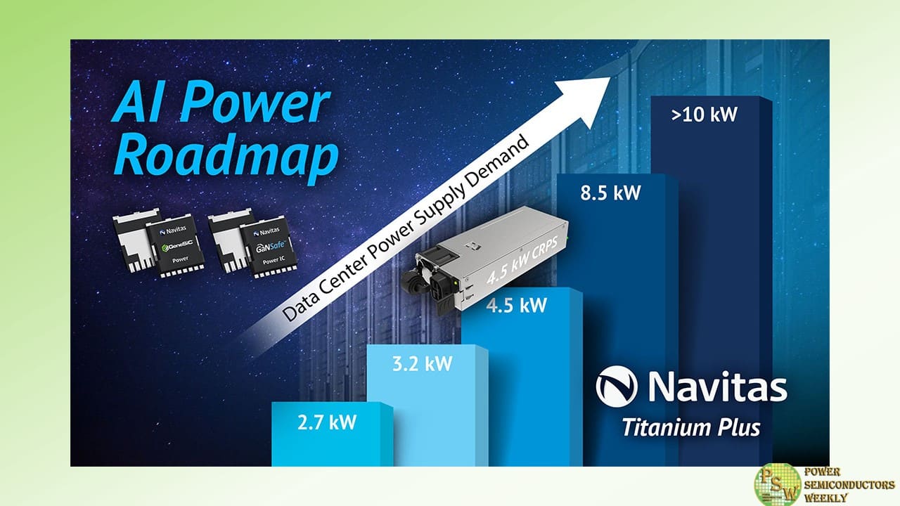
Navitas Semiconductor released its 4.5 kW AI data center power supply reference design, with optimized GaNSafe™ and Gen-3 ‘Fast’ (G3F) SiC power components. The optimized design enables the world’s highest power density with 137 W/in3 and over 97% efficiency.
Next-generation AI GPUs like NVIDIA’s Blackwell B100 and B200 each demand over 1 kW of power for high-power computation, 3x higher than traditional CPUs. These new demands are driving power-per-rack specifications from 30-40 kW up to 100 kW.
Navitas announced its AI Power Roadmap in March 2024, showcasing next-generation data center power solutions for the growing demand in AI and high-performance computing (HPC) systems. The first design was a GaNFast-based 3.2 kW AC-DC converter in the Common Redundant Power Supply (CRPS) form factor, as defined by the hyperscale Open Compute Project. The 3.2 kW CRPS185 (for 185 mm length) enabled a 40% size reduction vs. the equivalent legacy silicon approach and easily exceeded the ‘Titanium Plus’ efficiency benchmark, critical for data center operating models and a requirement for European data center regulations.
Now, the latest 4.5 kW CRPS185 design demonstrates how new GaNSafe™ power ICs and GeneSiC Gen-3 ‘Fast’ (G3F) MOSFETs enables the world’s highest power density and efficiency solution. At the heart of the design is an interleaved CCM totem-pole PFC using SiC with full-bridge LLC topology with GaN, where the fundamental strengths of each semiconductor technology are exploited for the highest frequency, coolest operation, optimized reliability and robustness, and highest power density and efficiency. The 650 V G3F SiC MOSFETs feature ‘trench-assisted planar’ technology which delivers world-leading performance over temperature for the highest system efficiency and reliability in real-world applications.
For the LLC stage, 650 V GaNSafe power ICs are ideal and unique in the industry with integrated power, protection, control, and drive in an easy-to-use, robust, thermally-adept TOLL power package. Additionally, GaNSafe power ICs offer extremely low switching losses, with a transient-voltage capability up to 800 V, and other high-speed advantages such as low gate charge (Qg), output capacitance (COSS), and no reverse-recovery loss (Qrr). High-speed switching reduces the size, weight, and cost of passive components in a power supply, such as transformers, capacitors, and EMI filters. As power density increases, next-gen GaN and SiC enable sustainability benefits, specifically CO2 reductions due to system efficiency increases and ‘dematerialization’.
The 3.2 kW and 4.5 kW platforms have already generated significant market interest with over 30 data center customer projects in development expected to drive millions in GaN and SiC revenue, ramping from 2024 into 2025.
Navitas’ AI data center power supply reference designs dramatically accelerate customer developments, minimize time-to-market, and set new industry benchmarks in energy efficiency, power density and system cost, enabled by GaNFast power ICs and GeneSiC MOSFETs. These system platforms include complete design collateral with fully tested hardware, embedded software, schematics, bills-of-material, layout, simulation, and hardware test results.
“AI is dramatically accelerating power requirements of data centers, processors and anywhere AI is going in the decades to come creating a significant challenge for our industry. Our system design center has stepped up to this challenge delivering a 3x increase in power in less than 18 months”, said Gene Sheridan, CEO of Navitas Semiconductor. “Our latest GaNFast technology, combined with our G3F SiC technology are delivering the highest power density and efficiency the world has ever seen…the perfect solution for the Blackwell AI processors and beyond.”
Original – Navitas Semiconductor
-

AIXTRON SE supports Nexperia B.V. in the ramp-up of its 200mm volume production for silicon carbide (SiC) and gallium nitride (GaN) power devices. With the new G10-SiC for the 200mm SiC volume ramp, Nexperia is placing a repeat order for AIXTRON SiC tools. This is complemented by an order for AIXTRON G10-GaN tools.
Both GaN and SiC epitaxial films are essential for the design of next-generation energy-efficient Field-Effect (FET) or Metal-Oxide-Field Effect (MOSFET) transistors to be used in various power conversion applications ranging from data centers and solar inverters in electric vehicles (EV) or trains.
Nexperia has decades of experience in the development of power devices, achieving more than 2.1 billion USD in revenue in 2023. After releasing its first GaN FET device in 2019 and its first SiC MOSFET in 2023, Nexperia continues to expand its portfolio with new high-reliability and power-efficient devices.
Nexperia, headquartered in Nijmegen (Netherlands), operates front-end factories in Hamburg (Germany) and Greater Manchester (England). The AIXTRON epitaxy systems will be installed at Nexperia’s wafer fab in Hamburg (Germany), further strengthening the semiconductor production capabilities in the region. Nexperia’s Hamburg site produces approximately 100 billion discrete semiconductors annually, accounting for about a quarter of the global production of this type of products.
“We are honored to strengthen our alliance with Nexperia, a pivotal player in the semiconductor landscape. Our G10 epitaxy solutions are at the heart of this collaboration, bolstering Nexperia’s growth strategies and enabling the high-volume production of wide bandgap semiconductors for commercial applications. Together, we are setting the pace for the industry’s transition to more energy-efficient SiC and GaN solutions”, said Dr. Felix Grawert, CEO and President of AIXTRON SE.
“As we advance our technological capabilities and market presence in high-power semiconductor production, our strategic partnership with AIXTRON is transformative. Integrating the G10 systems will significantly enhance our wide bandgap technology development and production capabilities. We build on AIXTRON’s proven uniformity and leverage the additional productivity gains of AIXTRON’s G10 tools to scale up our production efficiently and cost-effectively. With the new G10 tools in our Hamburg facility, we are poised for further advancements in our production capabilities,” said Achim Kempe, COO at Nexperia B.V.
Original – AIXTRON
-

Efficient Power Conversion (EPC) announced that it has moved one step closer to achieving preeminence in the gallium nitride (GaN) power semiconductor industry, as its intellectual property rights to this revolutionary technology were upheld for the third time in three months. The next-generation wide bandgap semiconductors developed by EPC are essential to artificial intelligence (AI), satellites, fast chargers, lidar, humanoid robots and many other transformational technologies.
The U.S. International Trade Commission (ITC) found two of EPC’s key patents valid and one, the Company’s foundational patent, infringed by Innoscience (Zhuhai) Technology Co., Ltd. and its affiliate, Innoscience America, Inc. The ITC’s recommendation comes on the heels of two recent decisions from the China National Intellectual Property Administration (CNIPA), which similarly validated EPC’s counterpart patents in China. The ITC initial determination is a significant milestone in solidifying EPC’s leadership in wide bandgap semiconductors and could lead to a ban later this year on importation of Innoscience’s infringing products into the United States.
“The ITC’s finding that Innoscience uses our patented technology without authorization puts EPC in an enviable position, as U.S. and Chinese regulatory bodies have upheld the validity of our patents,” said Alex Lidow, CEO and Co-Founder of EPC.
“The Commission’s recommendations validate nearly two decades of hard work, resources and R&D that went into developing EPC’s uniquely valuable intellectual property portfolio,” Dr. Lidow added.
Over the last 15 years, EPC has capitalized on its first-mover advantage to develop a broad portfolio of over 200 GaN-related patents and over 150 products, which include its rapidly growing family of integrated circuits, automotive qualified and radiation hardened devices.
Compared with traditional silicon-based power devices, GaN represents a significant leap, with higher efficiency, faster switching speeds, smaller size and lower cost. GaN power devices are integral to self-driving vehicles, medical and communications devices, next-generation rapid chargers, drones, satellites, data centers, e-bikes, solar power systems and humanoid robots, among many other applications. Most notably, EPC’s cutting-edge semiconductors are central to powering the AI revolution by significantly freeing up space for extra computing power while simultaneously reducing energy consumption.
The ITC’s preliminary ruling found both U.S. patents that EPC asserted against Innoscience valid. It also found “infringement [by Innoscience] of U.S. Patent No. 8,350,294,” EPC’s foundational patent used broadly across multiple industries. The second EPC patent, U.S. Patent No. 8,404,508, was found valid, but not infringed by Innoscience. The Commission’s final determination is expected to be issued on November 5, 2024.
Original – Efficient Power Conversion
-

The third edition of the second-level master’s program in “Power Electronics Devices and Technologies” organized by the Department of Electrical, Electronic and Information Engineering (DIEEI) of the University of Catania together with STMicroelectronics has been announced.
The goal of the master’s program is to train specialists in technologies based on Wide Band-Gap semiconductors, the new frontier of power electronics that ensures more efficient performance in line with the sustainable development goals defined by Agenda 2030. These technologies are for use in production processes in industries such as automotive, renewable energy, and electrical energy conversion and storage.
“There is a strong market demand for highly specialized professionals trained in the field of power electronics, to meet the needs identified by macro-trends in terms of energy efficiency and the electrification of mobility in the frame of sustainable development,”said Professor Mario Cacciato, coordinator of the master’s program.
“This second-level master’s program offers to master’s graduates in different STEM disciplines opportunities to complete the training and focus it on topics of great interest for research and industry. In addition, the master’s program constitutes a synergistic model for the professional development of young talent from academia together with the industrial world, as effectively demonstrated by the first two editions of the master’s program.”
“STMicroelectronics’ site in Catania is a center of excellence in the European arena for power electronics technologies, thanks in part to the strategic investment in the vertically integrated production of Silicon Carbide devices,” said Gianfranco Di Marco, Power Transistor Sub-Group, Chief of staff and Technical Communication Manager at STMicroelectronics.
“Training specialized profiles and skills in the field of power electronics with multidisciplinary knowledge is essential for fostering technological innovation. This third edition follows the success of the previous ones with theoretical lectures held at University of Catania and internships at ST’s Catania site allowing students to experience working with a leader in power semiconductors. This will forge a close connection between the world of education and the world of work, an essential prerequisite for the sustainable development of the area, and the creation of new career opportunities for students.”
The second-level master’s program offers theoretical and practical training, divided into 7 teaching modules in English. Lectures will be taught by university professors and appropriate specialists from within STMicroelectronics, who will also act as mentors during their internship in the company’s departments and research laboratories. Some lectures, moreover, will be held at ST’s Catania site. Finally, students will participate in seminars held by experts from several major world’s corporations in the industry.
The training course is open to those with a master’s degree obtained in the last five years in:
- Electronic engineering (LM/29);
- Electrical engineering (LM/28);
- Computer and information engineering (LM/32);
- Mechanical engineering (LM/33);
- Chemical engineering (LM22);
- Automation engineering (LM25);
- Telecommunications engineering (LM/27);
- Physics (LM17);
- Materials science and engineering (LM/53);
- Chemical sciences (LM/54);
Proficiency in English is required.
A maximum of 30 participants will be admitted to this master’s degree program. The top 10 in the eligible list will be awarded a scholarship. Those ranking from 11th to 20th will receive a contribution to the tuition fee. Applications must be submitted by September 30, 2024. More information is available here.
The Scientific Committee members are the University of Catania faculty members Mario Cacciato (coordinator), Giuseppe Compagnini, Guglielmo Guido Condorelli, Salvatore Mirabella, Salvatore Pennisi and Antonio Terrasi; and Giuseppe Arena, Michele Calabretta, Gianfranco Di Marco, Vincenzo Randazzo, Mario Saggio, Rosario Scollo, Filippo Scrimizzi and Gabriele Bellocchi of STMicroelectronics.
Original – STMicroelectronics
-

GlobalFoundries announced that it has acquired Tagore Technology’s proprietary and production proven Power Gallium Nitride (GaN) IP portfolio, a high-power density solution designed to push the boundaries of efficiency and performance in a wide range of power applications in automotive, internet of things (IoT) and artificial intelligence (AI) datacenter. As the digital world continues to evolve with technologies like Generative AI, GaN stands out as a pivotal solution for sustainable and efficient power management particularly in datacenters.
Today’s announcement reinforces GF’s commitment to large-scale manufacturing of GaN technology that offers a suite of benefits to help datacenters meet the increasing power demands while maintaining or improving power efficiency, reducing costs and managing heat generation. The acquisition expands GF’s power IP portfolio and broadens access to market leading GaN IP that will enable GF customers to quickly bring differentiated products to market. As a part of the acquisition, a team of experienced engineers from Tagore, dedicated to the development of GaN technology, will be joining GF.
“We are committed to being the foundation of our customers’ power applications today and for decades to come,” said Niels Anderskouv, chief business officer at GF. “With this acquisition, GF takes another step toward accelerating the availability of GaN and empowering our customers to build the next generation of power management solutions that will reshape the future of mobility, connectivity and intelligence.”
“The accelerating demand for more power efficient semiconductors is dramatically increasing, and Tagore has been at the forefront of developing disruptive solutions using GaN technology for a wide range of power devices,” said Amitava Das, co-founder and chief operating officer of Tagore Technology. “The team and I are excited to join GlobalFoundries to increase our focus on market-leading IP that will help address power design challenges and support the continued evolution of automotive, industrial and AI datacenter power delivery systems.”
In February 2024, GF was awarded $1.5 billion in direct funding under the U.S. CHIPS and Science Act, part of that investment is targeted towards enabling the high-volume manufacturing of critical technologies including GaN to securely produce more essential chips.
Combining this manufacturing capacity with the technical know-how of the Tagore team, GF is set to transform AI system efficiency, especially in edge or IoT devices, where reduced power consumption is critical.
“GlobalFoundries is at the forefront of technological advancements. With Tagore Technology joining the GF India team, we will further enhance our tech capabilities, particularly in emerging areas like GaN,” said Jitendra Chaddah, vice president and India country head at GF. “I welcome the Tagore team to GF, and I am excited about the work we will do as we continue to grow and strengthen our engineering capabilities together.”
Original – GlobalFoundries
