-

Cambridge GaN Devices (CGD) announced two new packages for the company’s ICeGaN™ family of GaN power ICs that offer enhanced thermal performance and simplify inspection. Variants of the well-proven DFN style, both packages are extremely rugged and reliable.
Developed for CGD, the DHDFN-9-1 (Dual Heat-spreader DFN) is a thin, dual-side cooled package with a small, 10×10 mm footprint and wettable flanks to simplify optical inspection. It offers low thermal resistance (Rth(JC), and can be operated with bottom-side, top-side and dual-side cooling, offering flexibility in design and out-performing the often-used TOLT package in top-side and, especially, dual-side cooled configurations.
The DHDFN-9-1 package has been designed with dual-gate pinout to facilitate optimal PCB layout and simple paralleling, enabling customers to address applications up to 6 kW with ease. The BHDFN-9-1 (Bottom Heat-spreader DFN) is a bottom-side cooled package, also with wettable flanks for easy inspection. Thermal resistance is 0.28 K/W, matching or exceeding other leading devices. Measuring 10×10 mm, the BHDFN is smaller than the commonly-used TOLL package yet shares a similar footprint, hence a common layout with TOLL-packaged GaN power ICs is possible for ease of use and evaluation.
Nare Gabrielyan | Product Marketing Manager, CGD
“These new packages are part of our strategy to enable customers to use our ICeGaN GaN power ICs at higher power levels. Servers, data centres, inverters/motor drives, micro-inverters and other industrial applications are all beginning to enjoy the power density and efficiency benefits that GaN brings, but they are also more demanding. Therefore, it is essential for such applications that devices are also rugged and reliable, and easy to design in. These attributes are inherent in ICeGaN, and are supported and extended by the new packages.”
Improving thermal resistance performance has several benefits. First, more power output is available at the same RDS(on) . Devices also run at cooler temperatures for the same power, so less heatsinking is required, resulting in reduced system costs. Lower operating temperatures also lead to higher reliability and longer lifetimes. Finally, if cost is the constraint for the application, designers can use a lower cost part with a higher RDS(on) and still achieve the required power output.
The new packages will be shown for the first time publicly at the upcoming PCIM exhibition on CGD’s booth # 7 643, Nürnberg Messe, Nuremberg, Germany, 11-13th June 2024.
Original – Cambridge GaN Devices
-
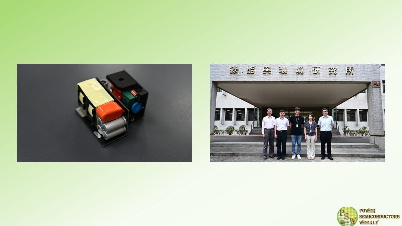
Cambridge GaN Devices (CGD) has signed a Memorandum of Understanding with Industrial Technology Research Institute (ITRI) of Taiwan to solidify a partnership in developing high performance GaN solutions for USB-PD adaptors. The MoU also covers the sharing of domestic and international market information, joint visits to potential customers and promotion.
Andrea Bricconi | Chief Commercial Officer, CGD
“We are excited to partner with ITRI, an organization with a power solution research team that is very experienced in developing power solutions and holds many patents. We will be demonstrating some of their board designs at our booth at the upcoming PCIM show in Nuremberg in June. These products utilize CGD’s unique IC chip architecture and ITRI’s patented designs to achieve product size reduction, high efficiency and power density, and cost competitiveness.”
Wen-Tien Tsai | leader of Commercial Power Design team, GEL/itri
“CGD’s IC-enhanced GaN – ICeGaN – is a novel platform that improves ease-of-use, facilitates smart temperature control and enhances gate reliability. We are excited to include these benefits in our new power designs.”
According to leading WBG analysts, Yole Group, the GaN market is expected to exceed $1B, with key growth in the applications of comms power supplies, and automotive DC/DC converters and on-board chargers. However, the first commercialized product in the market to adopt GaN devices has been USB-PD adaptors, and it is this market that the first designs from the partnership will address. Specifically, the agreement covers the development of power solutions in the 140-240 W range with power densities exceeding 30 W/in3 for e-mobility, power tools, notebook and cell phone applications.
Original – Cambridge GaN Devices
-

Infineon Technologies AG announced two new generations of high voltage (HV) and medium voltage (MV) CoolGaN TM devices which now enable customers to use Gallium Nitride (GaN) in voltage classes from 40 V to 700 V in a broader array of applications that help drive digitalization and decarbonization.
These two product families are manufactured on high performance 8-inch in-house foundry processes in Kulim (Malaysia) and Villach (Austria). With this, Infineon expands its CoolGaN advantages and capacity to ensure a robust supply chain in the GaN devices market, which is estimated to grow with an average annual growth rate (CAGR) of 46 percent over the next five years according to Yole Group.
“Today’s announcement builds nicely on our acquisition of GaN Systems last year and brings to market a whole new level of efficiency and performance for our customers,” said Adam White, Division President of Power & Sensor Systems at Infineon. “The new generations of our Infineon CoolGaN family in high and medium voltage demonstrate our product advantages and are manufactured entirely on 8 inch, demonstrating the fast scalability of GaN to larger wafer diameters. I am excited to see all of the disruptive applications our customers unleash with these new generations of GaN.”
The new 650 V G5 family addresses applications in consumer, data center, industrial and solar. These products are the next generation of GIT-based high voltage products from Infineon. The second new family manufactured on the 8-inch process is the medium voltage G3 devices which include CoolGaN Transistor voltage classes 60 V, 80 V, 100 V and 120 V; and 40 V bidirectional switch (BDS) devices. The medium voltage G3 products are targeted at motor drive, telecom, data center, solar and consumer applications.
The CoolGaN 650 V G5 will be available in Q4 2024 and the medium voltage CoolGaN G3 will be available in Q3 2024. Samples are available now.
Original – Infineon Technologies
-

The influence of artificial intelligence (AI) is driving up the energy demand of data centers across the globe. This growing demand underscores the need for efficient and reliable energy supply for servers. Infineon Technologies AG opens a new chapter in the energy supply domain for AI systems and unveils a roadmap of energy efficient power supply units (PSU) specifically designed to address the current and future energy need of AI data centers.
By introducing unprecedented PSU performance classes, Infineon enables cloud data center and AI server operators to reduce their energy consumption for system cooling. The innovative PSUs reduce power consumption and CO 2 emissions, resulting in lower lifetime operating costs. The powerful PSUs are not only used in future data centers but can also replace existing power supply units in servers and increase efficiency.
In addition to the current PSUs with an output of 3 kW and 3.3 kW available today, the new 8 kW and 12 kW PSUs will contribute to further increasing energy efficiency in future AI data centers. With the 12 kW reference board, Infineon will offer the world’s first power supply unit that achieves this level of performance and supplies future data centers with power.
“At Infineon, we power AI. We are addressing a critical question of our era – how to efficiently meet the escalating energy demands of data centers,” says Adam White, Division President Power & Sensor Systems at Infineon. “It’s a development that was only possible by Infineon’s expertise in integrating the three semiconductor materials silicon (Si), silicon carbide (SiC), and gallium nitride (GaN) into a single module. Our PSU portfolio is therefore not only an example of Infineon’s innovative strength, which leads to first-class results in terms of performance, efficiency and reliability for data centers and the AI ecosystem. It also reinforces Infineon’s market leadership in power semiconductors.”
Infineon is responding to the requirements of data center operators for higher system efficiency and lower downtimes. The growth of server and data center applications has led to an increase in power requirements, necessitating the development of power supplies with higher power ratings from 800 W up to 5.5 kW and beyond. This increase is driven by the growing power requirements of Graphic Process Units (GPU) on which AI applications are computed.
High-level GPUs now require up to 1 kW per chip reaching 2 kW and beyond by the end of the decade. This will lead to higher overall energy demand for data centers. Depending on the scenario, data centers will account for up to seven percent of global electricity consumption by 2030; this is an order of magnitude comparable to India’s current electricity consumption.
Infineon’s new PSUs contribute to the efforts to limit the CO 2 footprint of AI data centers despite the rapidly growing energy requirements. This is made possible by a particularly high level of efficiency that minimizes power losses. Infineon’s new generation PSUs achieve an efficiency of 97.5 percent and meet the most stringent performance requirements. The new 8 kW PSU is capable of supporting AI racks with an output of up to 300 kW and more. Efficiency and power density is increased to 100 watts per in³ compared to 32 W/in³ in the available 3 kW PSU, providing further benefits for the system size and cost savings for operators.
From a technical perspective, this is made possible by the unique combination of the three semiconductor materials Si, SiC and GaN. These technologies contribute to the sustainability and reliability of AI server and data center systems. Innovative semiconductors based on wide-bandgap materials such as SiC and GaN are the key to a conscious and efficient use of energy to drive decarbonization.
The 8 kW Power Supply Unit will be available in Q1 2025. For more information about the PSU roadmap, please click here.
Infineon at the PCIM Europe 2024
PCIM Europe will take place in Nuremberg, Germany, from 11 to 13 June 2024. Infineon will present its products and solutions for decarbonization and digitalization in hall 7, booths #470 and #169. Company representatives will also be giving several presentations at the accompanying PCIM Conference and Forums, followed by discussions with the speakers. Information about Infineon’s PCIM 2024 show highlights is available at www.infineon.com/pcim.
Original – Infineon Technologies
-

Transphorm, Inc. announced that its PCIM 2024 showcase will underscore its ability to outperform competitive wide bandgap technologies in higher power systems. For example, Transphorm’s normally-off d-mode SuperGaN®platform delivers higher electron mobility resulting in lower crossover losses versus Silicon Carbide—making it more a cost-effective, higher performing solution for various electric vehicle, datacenter/AI, infrastructure, renewable energy, and other broad industrial applications. To learn more, visit Transphorm during PCIM in Hall 7, Stall 108 during June 11 to 13, 2024.
Transphorm SuperGaN FETs are in production in a wide range of customer products crossing the power spectrum from low 45 W power adapters to higher power 7.5 kW PSUs. Many of these customer products are the first publicly recognized GaN-based systems of their kind and uniquely demonstrate advantages enabled only by the SuperGaN platform.
Examples include the previously mentioned liquid-cooled 7.5 kW PSU for mission-critical datacenter/blockchain applications; a 2.7 kW server CRPS with > 82 W/in3 power density (highest in any GaN power system available today); and 2.2 kW and 3 kW rack-mount 1U uninterruptible power supplies (UPSes). These design wins illustrate Transphorm’s ability to drive GaN into the various application markets composing an estimated GaN TAM of $8 billion by 2028.
In addition to real-world customer products, Transphorm continues to lead in technological achievements having recently demonstrated a 5 microsecond short-circuit withstand time, a bidirectional four-quadrant switch, and a 1200 V GaN-on-Sapphire device.
On-site demonstrations will include Transphorm solutions for 2- and 3-wheeler electric vehicle chargers along with customer PSUs for renewable energy systems, data centers, and more.
Speaking Engagement
Learn more about how Transphorm’s GaN solutions outperform competitive technologies and enable cross-industry innovations during the Bodo’s Power Systems session.
Panel: GaN Wide Bandgap Design, the Future of Power
Speaker: Philip Zuk, Senior Vice President, Business Development and Marketing
Date: June 12
Time: 2:20 – 3:20 p.m. CEST
Location: Hall 7, Stall 743Original – Transphorm
-
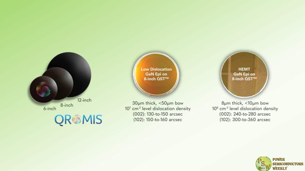
Qromis, Inc. brings a revolutionary, high performance substrate solution for large-diameter GaN epi and device wafers. Rather than solving incremental scale and performance challenges of conventional substrates for WBG semiconductors, QST™ (Qromis Substrate Technology) has been developed and validated as a disruptive solution, with cross-functional optimization.
In this approach, the key properties of substrate material such as stress, lattice mismatch, thermal stability and shape control are engineered independently for the best fit with GaN epitaxial and device layers, as well as with different device architectures and performance targets. QST™ materials layers are integrated together in the conventional semiconductor fab with a simple manufacturing flow.
The resulting large diameter substrates (6-inch, 8-inch, 12-inch or beyond) are capable of supporting from a few to tens of microns of high-quality GaN epitaxy, from which unique, high performance and low cost GaN device structures are fabricated.Qromis is designing reference devices for device manufacturers to demonstrate the benefits of the groundbreaking QST™ technology. These devices exploit key advantages of QST™ over other substrate solutions:
– High quality and stress-free GaN,
– Ability to deposit thick, bulk-like GaN epi layers on large diameter substrates,
– Low defectivity, eliminating a major limitation to performance and scalability.
With these distinct features, designers can now break free from the current technological limitations of GaN process technologies and develop advanced device architectures for lateral and vertical device designs of light emitters, switches, rectifiers, as well as monolithic and integrated circuits.Qromis, Inc., established in March 2015 and located in Silicon Valley, California, is a privately held fabless technology innovator focusing on energy efficient and high performance wide bandgap (WBG) semiconductor materials and device solutions which dramatically reduce global energy use and consumption. The Company is poised to become one of the premier players in the rapidly growing, multi-billion dollar WBG industry with its disruptive and validated solutions in substrate and device technologies, which enable an unmatched cost, performance, and application scale. Markets served include power electronics, light emitting diodes (LEDs), advanced displays, and RF electronics, and other emerging high performance and energy efficient applications.
As a fabless company, Qromis is driving the commercialization of its unique solutions in conjunction with its foundry network. The Company and its foundry partner offer WBG device foundry services, as well as access to advanced and novel process technology platforms, for its customers and partners.To learn more about Qromis and its substrate technology, join the International Conference on Compound Semiconductor Manufacturing Technology which takes place May 20-23, 2024 in Tucson, Arizona.
Original – Qromis
-

Power Integrations announced an agreement to acquire the assets of Odyssey Semiconductor Technologies, a developer of vertical gallium-nitride (GaN) transistor technology. The transaction is expected to close in July 2024, after which all key Odyssey employees are expected to join Power Integrations’ technology organization.
The acquisition supports the company’s ongoing development roadmap for its proprietary PowiGaN™ technology, which is featured in many of the company’s product families including InnoSwitch™ ICs, HiperPFS™-5 power-factor-correction ICs and the recently launched InnoMux™-2 family of single-stage, multiple-output ICs. The company introduced 900- and 1250-volt versions of PowiGaN technology and products in 2023.
Commented Dr. Radu Barsan, Power Integrations’ vice president of technology: “Power Integrations has been at the forefront of GaN development and commercialization since we began shipping products with PowiGaN technology in 2018. We are executing on an ambitious roadmap that includes driving toward cost parity with silicon MOSFETs and expanding the voltage and power capabilities of PowiGaN.
Our goal is to commercialize a cost-effective high-current and high-voltage GaN technology to support higher-power applications currently served by silicon carbide (SiC), at a much lower cost and higher performance enabled by the fundamental material advantages of GaN over SiC. The experience of the Odyssey team in high-current vertical GaN will augment and accelerate these efforts, and we are delighted to add them to our team.”
Added Dr. Richard Brown, Odyssey co-founder and CEO: “The Odyssey team and I are excited to join Power Integrations in accelerating their GaN technology roadmap. As the first company to commercialize high-voltage GaN, Power Integrations continues to lead the industry in driving the technology forward in terms of cost, voltage and current, as well as the design of system-level products that take full advantage of the capabilities of GaN.”
Original – Power Integrations
-

Transphorm, Inc. and the global leader in adapter USB Power Delivery (PD) Controller Integrated Circuits (IC) Weltrend Semiconductor Inc. announced availability of two new GaN System-in-Packages (SiPs). When combined with Weltrend’s flagship GaN SiP announced last year, the new devices establish the first SiP product family based on Transphorm’s SuperGaN® platform.
The new SiPs—WT7162RHUG24B and WT7162RHUG24C—integrate Weltrend’s high frequency multi-mode (QR/Valley Switching) Flyback PWM controller with Transphorm’s 150 mΩ and 480 mΩ SuperGaN FETs respectively. Like their 240 mΩ predecessor (WT7162RHUG24A), the devices pair with USB PD or programmable power adapter controllers to provide a total adapter solution.
Notably, they also offer several innovative features including the UHV valley tracking charge mode, adaptive OCP compensation, and adaptive green mode control among others that allow customers to design high quality power supplies faster and with fewer components using the simplest design approach.
“When we launched our first GaN SiP last year, it was an important milestone in our company’s evolution. It demonstrated a new GTM strategy for the AC-to-DC power market,” said Wayne Lo, Vice President of Marketing, Weltrend. “Today’s news confirms we’re continuing to serve that space with a wider selection of devices designed to support a wider assortment of product power levels. A total packaged solution with Transphorm’s SuperGaN platform delivers design simplicity with unparalleled performance for devices now ranging from low 30-watt USB-C PD power adapters through to nearly 200-watt chargers, a unique Transphorm GaN capability.”
End product manufacturers seek ways to develop new adapters with a reduced bill-of-materials (BOM) that offer versatility, fast charging, and higher power outputs. Additionally, in many cases they seek to deliver “one-size-fits-all” chargers with multiple ports and/or multiple types of connections. All of this in smaller, lighter weight form factor.
Some key advantages of Transphorm’s normally-off d-mode SuperGaN platform include best-in-class robustness (+/- 20 V gate margin with a 4 V noise immunity) and reliability (< 0.05 FIT) with the ability to increase power density by 50% over silicon. Weltrend’s elegant SiP designs harness those advantages along with its own innovative technologies to create a near plug-and-play solution that speeds design while reducing form factor size.
“SiPs are an important device option when considering the needs of adapter and charger manufacturers,” said Tushar Dhayagude, Vice President of Worldwide Sales and FAE, Transphorm. “These systems require effective power conversion that, while simple to use with integrated functionality, also minimize learning curves to ensure quick design in. The first device released validated the performance and versatility of a SuperGaN SiP. The new devices announced today validate both our companies’ deepening commitment to arming customers with choice.”
Key Specifications WT7162RHUG24A WT7162RHUG24B (new) WT7162RHUG24C (new) Rds(on) 240 mΩ 150 mΩ 480 mΩ Vds min 650 V Power Efficiency > 93% Power Density 26 w/in3 Max Frequency 180 kHz Wide Output
Voltage OperationUSB-C PD 3.0
PPS 3.3V~21VPackage 24-pin 8×8 QFN Key Features Feature Advantage Adjustable GaN FET gate slew rate control Balances out efficiency and EMI compliance External VDD linear regulator circuit not required
(700 V ultra HV start-up current pulled directly from AC Line voltage)Reduces component count Reduced package inductance Maximizes chip performance Fits in a standard 8×8 QFN FF Allows for low profile/small system footprint Original – Transphorm
-

Navitas Semiconductor announced that Virtual Forest, one of India’s leading electronics design companies specializing in motor control and human interface technologies for consumer appliances, fluid movement and mobility, has adopted its GaNFast™ power integrated circuits (IC) technology for a zero-emission, powerful 3 hp (2,250W) solar-powered irrigation pump.
For many farmers worldwide, irrigating remote crops requires powerful pumps to lift water from rivers and streams up to field-level, with the majority powered by polluting and noisy diesel generators or expensive, lossy long-distance electrical cables. The Virtual Forest solar pump with maximum power point tracking (MPPT) operates in conjunction with solar panel and energy storage to provide robust, energy-independent and pollution-free performance at the point of use.
The 3 hp (2,250W) pump is remotely accessed via quad-band IoT with low power consumption. It can raise over 50 gallons-per-minute of water to a height of over 90 feet, enough to water 3 acres of farmland, and help to produce 10 tonnes of wheat. Further, the IoT enabled solar pump ensures optimal water usage through intelligent analytics, therefore minimizing ground water utilization.
Navitas GaNSense™ half-bridge power ICs monolithically by integrating two GaN power FETs with GaN drivers, level-shifters, protection features and high-efficiency loss-less current sensing. High-efficiency NV6269 half-bridge ICs, in easy-to-use 8×10 mm QFN packages are used in a 3-phase motor inverter, with 3x-5x energy savings vs legacy silicon IGBTs.
“The $450 million solar-pump market in India is expected to reach $1.5 Bn by 2026, calling for a solar revolution on Indian fields,” said Virtual Forest’s CEO, Omer Basith, adding “Reliable, off-grid systems are critical to overcome food insecurity and achieve energy efficiency. Leveraging Navitas’ high-power, efficient GaNSense™ half-bridge, we seek to deliver a robust solution to the market. We are nurturing our dream to drive gigatons of reduction in carbon emissions, thereby making the world a greener place to live in. Hence, our name — Virtual Forest.”
“The design team at Virtual Forest adopted the GaNSense half-bridges very quickly, for a fast time-to-market,” said Alessandro Squeri, Navitas’ Senior Sales Director. “With GaNSense, ‘easy-to-use feature, Virtual Forest comes into the partnership with high efficiency, low component count and a robust design for tough environments.”
Original – Navitas Semiconductor
-

Chicony Power Technology, a worldwide leading manufacturer of power supplies and a pioneer in power electronics, has announced the winners of its Annual Partner Awards, honoring Infineon Technologies AG as its 2023 “GaN Strategic Partner of the Year”.
Infineon has been recognized by Chicony Power as its top partner for gallium nitride (GaN)-based power supplies, including notebook adapters, as well as ICT applications in gaming, storage and servers. This acknowledgment is the result of Infineon’s high standards for product selection, application expertise, high reliability and cost-effectiveness.
GaN stands out as one of the most crucial technologies which are essential for improving the efficiency of power supplies and reducing their product size. Pooling Infineon’s leading GaN expertise and Chicony Power’s remarkable capabilities in power supply system design, the win-win collaboration has helped push the boundaries of innovation and further strengthened both companies’ leading positions in energy-efficient power solutions. As of today, the GaN adoption rate in Chicony Power’s high-watt adapters has reached 20 percent, and this rate is rapidly increasing.
“Unrivalled R&D resources, a comprehensive application understanding and a large number of customer projects let Infineon continuously drive its roadmap for becoming a leading GaN Powerhouse,” said Adam White, Division President Power & Sensor Systems at Infineon Technologies. “The Strategic Partner of the Year award from Chicony Power is a great honor for us. We see this as part of our common mission to drive decarbonization and digitalization together.”
“We’re pleased to honor Infineon, which has played a pivotal role in driving customer success throughout 2023, as our GaN Strategic Partner of the Year,” said Peter Tseng, President of Chicony Power Technology. “Our Vision is to be a global pioneer in the implementation of new technology that enhances power supply efficiency, reduces the carbon footprint of power supplies and helps create a greener world. We would like our Annual Partner Awards to encourage Infineon and all other partners to maintain the momentum in jointly promoting GaN technology in the market alongside Chicony Power, making the power industry greener and cleaner.”
Original – Infineon Technologies
