-

At PCIM Europe 2024, Infineon Technologies AG will showcase how its latest semiconductor, software, and tooling solutions provide answers to today’s green and digital transformation challenges. Under the motto “Driving decarbonization and digitalization. Together.”, Infineon will demonstrate the industry’s broadest power electronics portfolio covering all relevant power technologies in silicon (Si), silicon carbide (SiC), and gallium nitride (GaN).
The company will be exhibiting in a larger area this year, with the main booth #740 in Hall 7 demonstrating innovative Si and SiC-based solutions, while the adjacent booth #169 is dedicated to the broad GaN portfolio. Alternatively, visitors can also register for Infineon’s digital event platform.
Infineon’s PCIM 2024 highlights
The products, demonstrations, and design aids on display illustrate how Infineon’s product-to-system expertise in power management enables engineers to balance operational specifications with application requirements. Demonstrations will include solutions from the following areas:
- Wide-bandgap technologies: Wide-bandgap materials are revolutionizing power electronics and various applications that are driving the green and digital transformation. Infineon will demonstrate the CoolSiC™ MOSFETs 650 V and 1200 V Generation 2, which can be used to improve overall energy efficiency. Additionally, the expanded portfolio of GaN solutions will be showcased, offering a wide range of innovative packages, discrete and integrated solutions.
- Renewables, energy storage and HVDC: With its power solutions, Infineon enables the most climate-friendly forms of energy generation from wind and solar accompanied by efficient storage systems. At PCIM, the company will present a wide range of solutions for single-phase and three-phase hybrid solar inverters as well as its In-Field Power Analytics Service helping to maximize converter uptime and optimize operation in real-time.
- Industrial automation, motor drives and control: With advanced power semiconductors, Infineon is paving the way for highly reliable and energy-efficient electric motors and drive solutions in smart factories. This is achieved through a combination of efficient energy management and intelligent motor control solutions, advanced sensor functions, and reliable connectivity components. Furthermore, the company is presenting its growing range of solid-state relays and circuit breakers as well as a stack assembly solution for high-end Press Pack IGBTs.
- Information and communication technologies: True to the motto “We power AI”, Infineon exhibits innovative technologies that make it possible to meet increasing energy demands while promoting greener AI and paving the way for more efficient AI servers. This includes two-phase power supply modules, integrated point-of-load solutions, and converters. In addition, the company will showcase cutting-edge solutions, including Si, SiC, and GaN power switches, that meet the evolving needs of server technology and telecoms networks, driving efficiency, reliability, and innovation across all industries.
- eMobility, eTransportation and charging solutions: With leading power supply solutions for traction inverters, on-board chargers, DC-DC converters, and battery management systems, Infineon supports the efforts of developers and manufacturers, enabling the rapid expansion of eMobility, eTransportation, eCAV, and the corresponding charging infrastructure. Highlights presented in this area include traction inverters with fusion, single-side cooling and discrete concepts, traction inverter systems for commercial vehicles and rail transport, as well as high power fast charging solutions.
- Smart and connected homes: Infineon’s leading technology portfolio of customized, ready-to-use solutions assists manufacturers in developing innovative system designs for homes that meet the growing demand for smart, connected, and energy-efficient living solutions. Highlights in this area include USB-C charging solutions, portable battery-powered welding solutions, residential heat pumps, as well as air conditioning systems.
Infineon will also contribute to the PCIM conference program and the various forums, including a keynote by Dr. Gerald Deboy, Fellow at Infineon, on the “Challenges and Solutions to Power Latest Processor Generations for Hyper Scale Data Centers” on June 13 at 8:45 am. An overview of all contributions by Infineon experts is available at www.infineon.com/pcim.
Original – Infineon Technologies
-
With the increasing power requirements of Artificial Intelligence (AI) processors, server power supplies (PSUs) must deliver more and more power without exceeding the defined dimensions of the server racks. This is driven by a surge in energy demand of high-level GPUs, which could consume 2 kW and more per chip by the end of the decade.
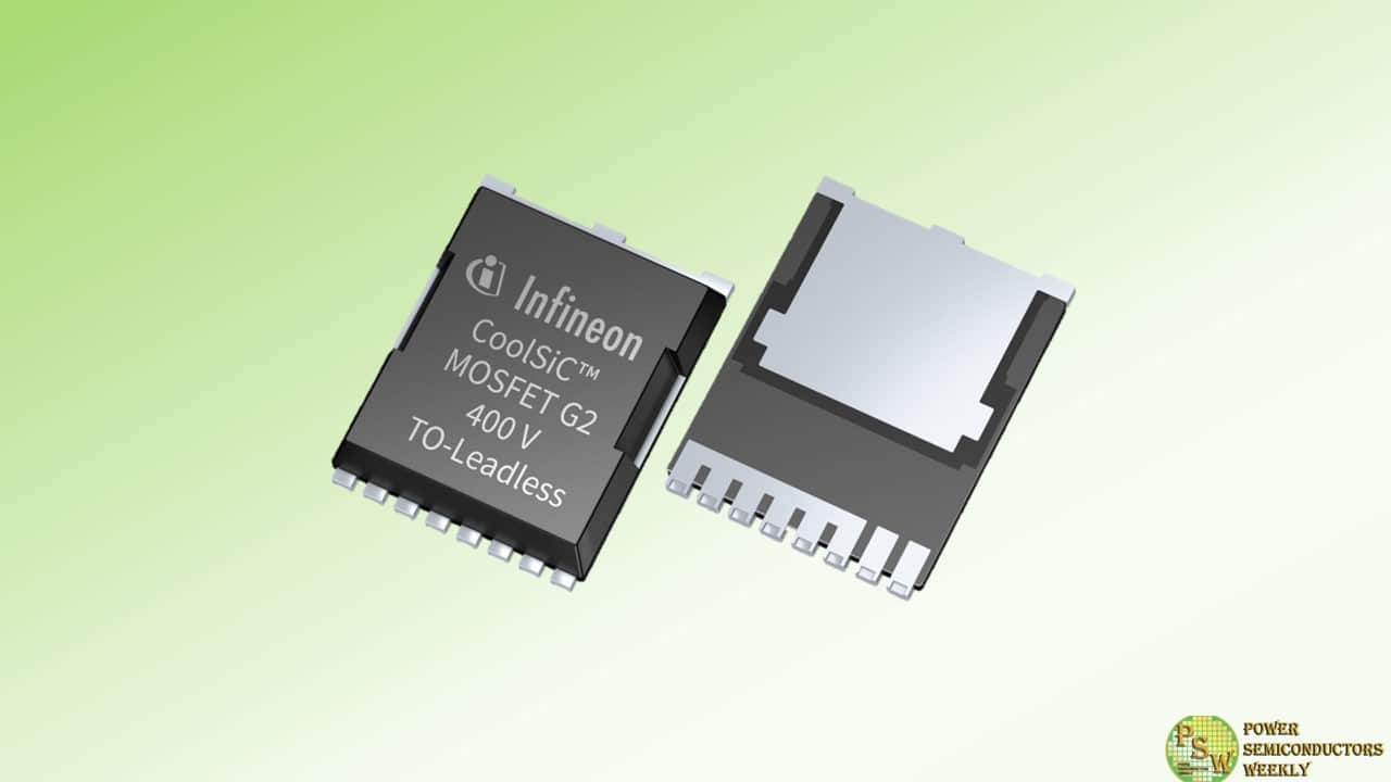
These needs, as well as the emergence of increasingly demanding applications and the associated specific customer requirements have prompted Infineon Technologies AG to extend the development of SiC MOSFETs to voltages below 650 V. The company is now launching the new CoolSiC™ MOSFET 400 V family, which is based on the second generation (G2) CoolSiC technology introduced earlier this year.
The new MOSFET portfolio was specially developed for use in the AC/DC stage of AI servers, complementing Infineon’s recently announced PSU roadmap. The devices are also ideal for solar and energy storage systems (ESS), inverter motor control, industrial and auxiliary power supplies (SMPS) as well as solid-state circuit breakers for residential buildings.
“Infineon offers an extensive portfolio of high-performance MOSFETs and GaN transistors to meet the demanding design and space requirements of AI server power supplies”, said Richard Kuncic, Head of the Power Systems Business Line at Infineon. “We are committed to supporting our customers with advanced products such as the CoolSiC MOSFETs 400 V G2 to drive highest energy efficiency in advanced AI applications.”
The new family features ultra-low conduction and switching losses when compared to existing 650 V SiC and Si MOSFETs. Implemented in a multi-level PFC, the AC/DC stage of the AI Server PSU can attain a power density of more than 100 W/in³ and is proven to reach 99.5 percent efficiency.
This is an efficiency improvement of 0.3 percentage points over solutions using 650 V SiC MOSFETs. In addition, the system solution for AI Server PSUs is completed by implementing CoolGaN™ transistors in the DC/DC stage. With this combination of high-performance MOSFETs and transistors, the power supply can deliver more than 8 kW with an increase in power density by a factor of more than 3 compared to current solutions.
The new MOSFET portfolio comprises a total of 10 products: five R DS(on) classes from 11 to 45 mΩ in Kelvin-source TOLL and D²PAK-7 packages with .XT package interconnect technology. The drain-source breakdown voltage of 400 V at T vj = 25°C. makes them ideal for use in 2- and 3-level converters and for synchronous rectification.
The components offer high robustness under harsh switching conditions and are 100 percent avalanche tested. The highly robust CoolSiC technology in combination with the .XT interconnect technology enables the devices to cope with power peaks and transients caused by sudden changes in the power requirements of the AI processor. Both the connection technology and a low and positive R DS(on) temperature coefficient enable excellent performance under operating conditions with higher junction temperatures.
Original – Infineon Technologies
-
The influence of artificial intelligence (AI) is driving up the energy demand of data centers across the globe. This growing demand underscores the need for efficient and reliable energy supply for servers. Infineon Technologies AG opens a new chapter in the energy supply domain for AI systems and unveils a roadmap of energy efficient power supply units (PSU) specifically designed to address the current and future energy need of AI data centers.
By introducing unprecedented PSU performance classes, Infineon enables cloud data center and AI server operators to reduce their energy consumption for system cooling. The innovative PSUs reduce power consumption and CO 2 emissions, resulting in lower lifetime operating costs. The powerful PSUs are not only used in future data centers but can also replace existing power supply units in servers and increase efficiency.
In addition to the current PSUs with an output of 3 kW and 3.3 kW available today, the new 8 kW and 12 kW PSUs will contribute to further increasing energy efficiency in future AI data centers. With the 12 kW reference board, Infineon will offer the world’s first power supply unit that achieves this level of performance and supplies future data centers with power.
“At Infineon, we power AI. We are addressing a critical question of our era – how to efficiently meet the escalating energy demands of data centers,” says Adam White, Division President Power & Sensor Systems at Infineon. “It’s a development that was only possible by Infineon’s expertise in integrating the three semiconductor materials silicon (Si), silicon carbide (SiC), and gallium nitride (GaN) into a single module. Our PSU portfolio is therefore not only an example of Infineon’s innovative strength, which leads to first-class results in terms of performance, efficiency and reliability for data centers and the AI ecosystem. It also reinforces Infineon’s market leadership in power semiconductors.”
Infineon is responding to the requirements of data center operators for higher system efficiency and lower downtimes. The growth of server and data center applications has led to an increase in power requirements, necessitating the development of power supplies with higher power ratings from 800 W up to 5.5 kW and beyond. This increase is driven by the growing power requirements of Graphic Process Units (GPU) on which AI applications are computed.
High-level GPUs now require up to 1 kW per chip reaching 2 kW and beyond by the end of the decade. This will lead to higher overall energy demand for data centers. Depending on the scenario, data centers will account for up to seven percent of global electricity consumption by 2030; this is an order of magnitude comparable to India’s current electricity consumption.
Infineon’s new PSUs contribute to the efforts to limit the CO 2 footprint of AI data centers despite the rapidly growing energy requirements. This is made possible by a particularly high level of efficiency that minimizes power losses. Infineon’s new generation PSUs achieve an efficiency of 97.5 percent and meet the most stringent performance requirements. The new 8 kW PSU is capable of supporting AI racks with an output of up to 300 kW and more. Efficiency and power density is increased to 100 watts per in³ compared to 32 W/in³ in the available 3 kW PSU, providing further benefits for the system size and cost savings for operators.
From a technical perspective, this is made possible by the unique combination of the three semiconductor materials Si, SiC and GaN. These technologies contribute to the sustainability and reliability of AI server and data center systems. Innovative semiconductors based on wide-bandgap materials such as SiC and GaN are the key to a conscious and efficient use of energy to drive decarbonization.
The 8 kW Power Supply Unit will be available in Q1 2025. For more information about the PSU roadmap, please click here.
Infineon at the PCIM Europe 2024
PCIM Europe will take place in Nuremberg, Germany, from 11 to 13 June 2024. Infineon will present its products and solutions for decarbonization and digitalization in hall 7, booths #470 and #169. Company representatives will also be giving several presentations at the accompanying PCIM Conference and Forums, followed by discussions with the speakers. Information about Infineon’s PCIM 2024 show highlights is available at www.infineon.com/pcim.
Original – Infineon Technologies
-
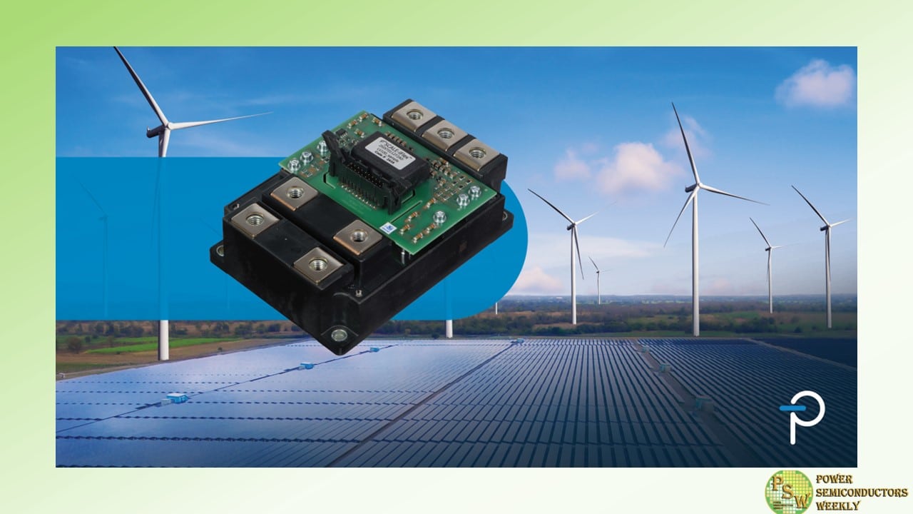
Power Integrations announced the launch of the SCALE-iFlex™ XLT family of dual-channel plug-and-play gate drivers for operation of single LV100 (Mitsubishi), XHP™ 2 (Infineon), HPnC (Fuji Electric) and equivalent semiconductor modules up to 2300 V blocking voltage for wind, energy storage and solar renewable energy installations.
This single-board driver enables active thermal management of inverter modules for improved system utilization and reduces the bill-of-material count for increased reliability.
Thorsten Schmidt, product marketing manager at Power Integrations commented: “It’s a real challenge to build a single-board gate driver for these ‘new dual’ style IGBT modules. Our compact new SCALE-iFlex XLT gate drivers fit inside the outline of the module, allowing the drivers to be mounted on the module, which gives converter system designers a high degree of mechanical design freedom.”
SCALE-iFlex XLT dual-channel gate drivers feature Negative Temperature Coefficient (NTC) data reporting – an isolated temperature measurement of the power module – which allows accurate thermal management of converter systems. This enables system designers to optimize thermal design and obtain a 25 to 30 percent converter power increase from the same hardware.
The isolated NTC readout also reduces hardware complexity, eliminating multiple cables, connectors and additional isolation barrier crossing circuits. The new gate drivers employ Power Integrations’ SCALE-2 chip set which minimizes component count, enhancing reliability. The gate driver board also protects the power switches in the event of a short-circuit.
Original – Power Integrations
-

Infineon Technologies AG Supervisory Board has extended the contract of Dr. Rutger Wijburg (62), Management Board member and Chief Operations Officer, for a period of one year, until 31 March 2026. In addition, the Supervisory Board will extend the contract of Andreas Urschitz (52), Management Board member and Chief Marketing Officer, for a period of five years, until 31 May 2030. The current contract of Andreas Urschitz expires at the end of May 2025; Rutger Wijburg’s contract would otherwise have expired in March 2025.
“Andreas Urschitz and Rutger Wijburg have played a decisive role in charting a course of profitable growth for Infineon. We are pleased that they will both continue as members of the Infineon Management Board in the upcoming years,” says Dr. Herbert Diess, Chairman of the Supervisory Board of Infineon Technologies AG. He adds that the Supervisory Board particularly respects the personal decision by Rutger Wijburg to extend his contract only until March 2026.
Andreas Urschitz has been a member of the Management Board since 2022, prior to which he was President of the Infineon Power & Sensor Systems (PSS) Division. Rutger Wijburg has been a member of the Management Board and Infineon’s Chief Operations Officer since 2022; he was previously Head of Frontend as well as Managing Director at Infineon Dresden.
Original – Infineon Technologies
-

Infineon Technologies AG reported the results for the second quarter of the 2024 fiscal year (period ended 31 March 2024).
- Q2 FY 2024: Revenue €3.632 billion, Segment Result €707 million, Segment Result Margin 19.5 percent
- Outlook for FY 2024: Based on an assumed exchange rate of US$1.10 to the euro, Infineon now expects to generate revenue of around €15.1 billion plus or minus €400 million (previously €16 billion plus or minus €500 million), with a Segment Result Margin of around 20 percent (previously in the low to mid-twenties percentage range) at the mid-point of the guided revenue range. Adjusted gross margin will be in the low-forties percentage range (previously in the low to mid-forties percentage range). Investments are planned at around €2.8 (previously around 2.9 billion). Adjusted Free Cash Flow of about €1.6 billion (previously €1.8 billion) and reported Free Cash Flow of about €0 million (previously about €200 million) are now expected
- Outlook for Q3 FY 2024: Based on an assumed exchange rate of US$1.10 to the euro, revenue of around €3.8 billion expected. On this basis, the Segment Result Margin is forecast to be in the high-teens percentage range
„In the prevailing difficult market environment, Infineon delivered a solid second quarter”, says Jochen Hanebeck, CEO of Infineon. “Many end markets have remained weak due to economic conditions, while customers and distributors have continued to reduce semiconductor inventory levels. Weak demand for consumer applications persists. There has also been a noticeable deceleration in growth in the automotive sector. We are therefore taking a cautious approach to the outlook for the rest of the fiscal year and are lowering our forecast. In the medium to long term, decarbonization and digitalization will continue to be strong structural drivers of our profitable growth. In order to realize the full potential of our Company, we will further strengthen our competitiveness. To this end, we are launching the company-wide “Step Up” program. We are aiming to achieve structural improvements in our Segment Result in the high triple-digit million euro range per year.”
For the full version of this news release (incl. financial data), please download the PDF version.
Original – Infineon Technologies
-
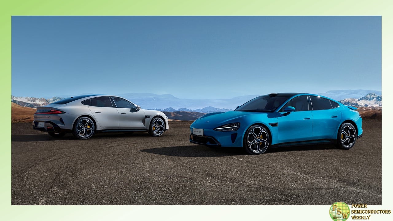
Infineon Technologies AG will provide silicon carbide (SiC) power modules HybridPACK™ Drive G2 CoolSiC™ and bare die products to Xiaomi EV for its recently announced SU7 until 2027. Infineon’s CoolSiC-based power modules allow for higher operating temperatures, resulting in best-in-class performance, driving dynamics and lifetime.
Traction inverters based on the technology can, for example, further increase electric vehicle range. The HybridPACK Drive is Infineon’s market-leading power module family for electric vehicles, with almost 8.5 million units sold since 2017.
Infineon provides two HybridPACK Drive G2 CoolSiC 1200 V modules for the Xiaomi SU7 Max. In addition, Infineon supplies Xiaomi EV with a broad range of products per car, including, for example, EiceDRIVER TM gate drivers and more than ten microcontrollers in various applications. The two companies also agreed to further cooperate on SiC automotive applications to fully utilize the benefits of Infineon’s SiC portfolio.
Zhenyu Huang, Vice President of Xiaomi EV and General Manager of the Supply Chain Department, said: “Infineon is an important partner with leading technologies and resilient manufacturing capabilities in power semiconductors as well as a highly scalable microcontroller product portfolio. The cooperation between the two companies will not only help stabilize the supply of silicon carbide for Xiaomi EV, but also help us build a high-performance, safe and reliable luxury car with leading-edge features for our customers.”
Peter Schiefer, President of Infineon’s Automotive division, said: “We are very pleased to work with dynamic players such as Xiaomi EV and provide them with silicon carbide products designed to enhance the performance of electric cars even further. As the leading partner to the automotive industry, we are well positioned with our broad product portfolio, system understanding and multi-site manufacturing base to shape the mobility of the future.”
This collaboration contributes to Infineon’s position as the number one partner of the global automotive industry. According to the latest data from TechInsights, Infineon is the largest semiconductor supplier to the automotive industry. In addition to its number one position in automotive power semiconductors, Infineon also took the lead in the field of automotive microcontrollers last year.
Original – Infineon Technologies
-
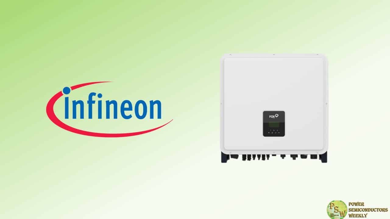
Infineon Technologies AG supplies its power semiconductor devices to FOXESS, a fast-growing leader in the green energy industry and a manufacturer of inverters and energy storage systems. The two sides aim at promoting the development of green energy.
Infineon will provide FOXESS with its CoolSiC™ MOSFETs 1200 V, which will be used with EiceDRIVER™ gate drivers for industrial energy storage applications. At the same time, FOXESS’ string PV inverters will use Infineon’s IGBT7 H7 1200 V power semiconductor devices.
The global market for photovoltaic energy storage systems (PV-ES) has grown at a high speed in the last years. As competition in the PV-ES market accelerates, improving power density has become key to success, and how to improve efficiency and power density for energy storage applications has attracted much attention. Infineon’s CoolSiC MOSFET 1200 V and IGBT7 H7 1200 V series power semiconductor devices adopt the latest semiconductor technologies and design concepts that are tailored to industrial applications.
Mr. Yu Daihui, Senior Vice President and Head of Industrial & Infrastructure of Infineon Technologies Greater China said, “As an industry leader in power semiconductors, we are proud to work closely with FOXESS. We will continue to drive decarbonization by enabling higher power density and more reliable systems for PV-ES applications.”
Mr. Zhu Jingcheng, Chairman of FOXESS, said, “Thanks to the support of Infineon’s advanced components, FOXESS’ products have been significantly improved in terms of reliability and efficiency. This has been an important driving force for FOXESS’ growth. Infineon’s technical support and product quality have not only strengthened our competitiveness, but also expanded our presence in the market. We are confident about the future and look forward to further cooperation with Infineon to jointly promote the development of the industry and create greater value for our customers.”
With a high power density, Infineon’s CoolSiC MOSFETs 1200 V can reduce losses by 50 percent and provide ~2 percent additional energy without increasing the battery size, which is especially beneficial for high-performance, lightweight, and compact energy storage solutions. FOXESS’ H3PRO 15 kW-30 kW energy storage series uses Infineon’s CoolSiC MOSFETs 1200 V for all models. Thanks to Infineon’s excellent performance, the H3PRO series has achieved an efficiency of up to 98.1 percent and excellent EMC performance; with superior performance and reliability, the H3PRO series has seen rapid sales growth in the global market.
Infineon’s TRENCHSTOP IGBT7 H7 650 V / 1200 V series has lower losses and helps improve the overall efficiency and power density of inverters. In high-power inverter projects, high-current mold packaged discrete devices with current handling capability above 100 A can reduce the number of IGBTs in parallel and replace the IGBT module solution, further improving system reliability and reducing costs; in addition, the H7 series has become an industry benchmark for its high-quality performance and greater resistance to humidity.
At present, FOXESS’ main industrial and commercial model, the R Series 75-110 kW, redefines the overall design of the 100 kW model by using IGBT7 H7 series discretes, and the efficiency of the whole machine can reach up to 98.6 percent. Thanks to the low power loss and high power density of the IGBT7 H7 series in discrete packages, technical problems such as current sharing in the paralleling process can be simplified and optimized.
Every power device needs a driver, and the right driver can make the design a lot easier. Infineon offers more than 500 EiceDRIVER gate drivers with typical output currents of 0.1 A~18 A and comprehensive protection functions including fast short-circuit protection (DESAT), active Miller clamp, shoot-through protection, fault reporting, shutdown, and overcurrent protection, suitable for all power devices including CoolSiC and IGBTs.
Original – Infineon Technologies
-
Chicony Power Technology, a worldwide leading manufacturer of power supplies and a pioneer in power electronics, has announced the winners of its Annual Partner Awards, honoring Infineon Technologies AG as its 2023 “GaN Strategic Partner of the Year”.
Infineon has been recognized by Chicony Power as its top partner for gallium nitride (GaN)-based power supplies, including notebook adapters, as well as ICT applications in gaming, storage and servers. This acknowledgment is the result of Infineon’s high standards for product selection, application expertise, high reliability and cost-effectiveness.
GaN stands out as one of the most crucial technologies which are essential for improving the efficiency of power supplies and reducing their product size. Pooling Infineon’s leading GaN expertise and Chicony Power’s remarkable capabilities in power supply system design, the win-win collaboration has helped push the boundaries of innovation and further strengthened both companies’ leading positions in energy-efficient power solutions. As of today, the GaN adoption rate in Chicony Power’s high-watt adapters has reached 20 percent, and this rate is rapidly increasing.
“Unrivalled R&D resources, a comprehensive application understanding and a large number of customer projects let Infineon continuously drive its roadmap for becoming a leading GaN Powerhouse,” said Adam White, Division President Power & Sensor Systems at Infineon Technologies. “The Strategic Partner of the Year award from Chicony Power is a great honor for us. We see this as part of our common mission to drive decarbonization and digitalization together.”
“We’re pleased to honor Infineon, which has played a pivotal role in driving customer success throughout 2023, as our GaN Strategic Partner of the Year,” said Peter Tseng, President of Chicony Power Technology. “Our Vision is to be a global pioneer in the implementation of new technology that enhances power supply efficiency, reduces the carbon footprint of power supplies and helps create a greener world. We would like our Annual Partner Awards to encourage Infineon and all other partners to maintain the momentum in jointly promoting GaN technology in the market alongside Chicony Power, making the power industry greener and cleaner.”
Original – Infineon Technologies
-

Infineon Technologies AG continued to expand its leading market position in automotive semiconductors in 2023. According to the latest research by TechInsights, the global automotive semiconductor market grew by 16.5 percent in 2023, reaching a new record size of US$69.2 billion.
Infineon’s overall market share increased by one percentage point, from nearly 13 percent in 2022 to about 14 percent in 2023, solidifying the company’s position as the global leader in the automotive semiconductor market. Infineon’s semiconductors are essential in serving all automotive key applications like driver assist and safety systems, powertrain and battery management, comfort, infotainment and security.
According to TechInsights, Infineon has increased its market share in all regions and remained market leader in South Korea and China. In addition, Infineon has made significant gains in the Japanese automotive semiconductor market. Infineon has strengthened its strong European presence as the second-largest player, as well as its top three position in North America.
“We are very proud that we have expanded our position as the leading automotive semiconductor supplier. This great success is based on our product innovation and system competence that add value to our customers’ solutions,” said Peter Schiefer, President of the Automotive Division at Infineon. “We also see this achievement as motivation, since our automotive semiconductors are the basis for the future of mobility, making cars clean, safe and smart.”
“Infineon maintained the top spot in the TechInsights automotive semiconductor 2023 vendor market share rankings with nearly 14 percent market share,” said Asif Anwar, Executive Director of Automotive End Market Research at TechInsights. “The company’s automotive semiconductor revenues grew over 26 percent year-on-year, allowing the company to stretch its lead over its second and third place rivals by four percentage points.”
A major driver of Infineon’s performance was strong automotive microcontroller (MCU) sales. For the first time, Infineon has reached the world’s number one position in this market. The company’s sales in the automotive microcontroller segment increased by nearly 44 percent compared to 2022, resulting in a 2023 market share of about 29 percent worldwide.
Microcontrollers are key components in the automotive industry, controlling and monitoring a wide variety of systems in the automobile such as electric powertrain, electric-electronic (E/E) architecture, advanced driver assistance systems (ADAS) and automated driving, radar and chassis.
Infineon’s AURIX™ flagship microcontroller family and the TRAVEO™ microcontroller family are the main contributors to this success, driving the transition in the automotive industry towards autonomous, connected and electrified vehicles. The families combine power and performance enhancements with the latest trends in the fields of virtualization, AI-based modeling, functional safety, cybersecurity and network functions. They are paving the way for new E/E architectures as well as the next generation of software-defined vehicles.
Original – Infineon Technologies
