-

X-FAB Silicon Foundries SE has launched XSICM03, its next-generation XbloX platform, advancing Silicon Carbide (SiC) process technology for power MOSFETs, delivering significantly reduced cell pitch, enabling increased die per wafer and improved on-state resistance without compromising reliability.
XbloX is X-FAB’s streamlined business process and technology platform designed to accelerate the development of advanced SiC MOSFET technology. It integrates qualified SiC process development blocks and modules for planar MOSFET production, simplifying the onboarding process and significantly reducing design risks and product development time.
By combining proven process modules with robust design rules, control plans, and FMEAs, XbloX enables faster prototyping, easier design evaluation, and shorter time to market. This approach gives customers a competitive edge, allowing designers to create a diverse product portfolio while achieving production timelines up to nine months faster than traditional development methods.
This next generation platform provides active area design cell size reduction while maintaining robust process controls, as well as leakage and breakdown device performance. The XSICM03 platform with robust design rules allows customers to create SiC planar MOSFETs with a cell pitch that is over 25% smaller than the previous generation.
This improvement allows for up to a 30% increase in die per wafer compared to the previous generation. Leveraging proven process blocks, the platform ensures exceptional gate oxide reliability and device robustness. The enriched PCM library and enhanced design support allow for fast customer tape-out, resulting in faster product development.
Rico Tillner, CEO, X-FAB Texas explains: “With its streamlined approach, our next-generation process platform addresses the increasing demand for high-performance SiC devices in automotive, industrial, and energy applications. We enable existing and new customers in creating application-optimized product portfolios through accelerated prototyping and design evaluation, significantly reducing time to market.”
The next generation platform XSICM03 is now available for early access.
Original – X-FAB Silicon Foundries
-

Nexperia announced the launch of 16 new 80 V and 100 V power MOSFETs in the innovative copper-clip CCPAK1212 package, delivering industry-leading power density and outright performance. The innovative copper-clip design provides high current conduction, reduced parasitic inductance, and excellent thermal performance. These features make the devices ideal for motor control, power supplies, renewable energy systems, and other power-hungry applications.
The range also includes application-specific MOSFETs (ASFETs) designed for AI server hot-swap functions. With top-side and bottom-side cooling options, these MOSFETs in CCPAK provide high power density and reliable solutions. All devices are supported by JEDEC registration and Nexperia’s interactive datasheets for seamless integration.
The benchmark PSMN1R0-100ASF is a 0.99 mΩ 100 V power MOSFET capable of conducting 460 A and dissipating 1.55 KW of power, yet in a CCPAK1212 package footprint that occupies only 12mm x 12mm of board space. The PSMN1R0-100CSF offers similar statistics in a top-side cooled version.
The secret to this impressive performance is the internal construction of the devices. The “CC” in CCPAK1212 stands for copper clip, meaning that the power MOSFET silicon die is sandwiched between two pieces of copper, the drain tab on one side and the source clip on the other. With wire bonds entirely eliminated, such an optimized assembly offers a low on-resistance, reduced parasitic inductances, high maximum current ratings and excellent thermal performance.
CCPAK1212 NextPower 80/100 V MOSFETs are recommended for power-hungry industrial applications where high efficiency and high reliability are critical, including brushless DC (BLDC) motor control, switched-mode power supplies (SMPS), battery management systems (BMS) and renewable energy storage. The availability of such power-capable MOSFETs in a single package reduces the need for parallelism, simplifying designs and offering more compact, cost-effective solutions.
The Nexperia CCPAK1212 announcement also includes some new application specific MOSFETs (ASFETs) targeting the hot-swap function in increasingly powerful AI servers. These devices feature an enhanced safe operating area (SOA), providing superior thermal stability during linear mode transitions.
Across all these applications, the availability of top-side and bottom-side cooling options provides engineers a choice of thermal extraction techniques, especially helpful where dissipating heat through the PCB is impractical due to the sensitivity of other components.
“Despite offering market-leading performance, we know that some customers will be reticent to design-in a relatively new package”, stated Chris Boyce, Product Group General Manager at Nexperia. “For this reason, we have registered the CCPAK1212 with the JEDEC standards organization (reference MO-359). We followed a similar approach when we introduced the first LFPAK MOSFET package some years ago and as a result there are now many compatible devices available in the market. You are never on your own for long when your innovations offer genuine value to your customers”, concluded Boyce.
All the new CCPAK1212 MOSFET devices are supported with a range of advanced design-in tools, including thermally compensated simulation models. Traditional PDF datasheets are supplemented with Nexperia’s user-friendly interactive datasheets, which now incorporate a new “graph-to-csv” feature that allows engineers to download, analyze and interpret the data behind each device’s key characteristics. This not only streamlines the design process but enhances confidence in design choices.
Nexperia plans to extend CCPAK1212 packaging to power MOSFETs across all voltage ranges and also to its automotive qualified AEC-Q101 portfolios, addressing the evolving demands of next-generation systems with the highest current and thermal performance requirements.
Original – Nexperia
-

To provide higher efficiency and power density for telecom, industrial, and computing applications, Vishay Intertechnology, Inc. introduced a new 150 V TrenchFET® Gen V n-channel power MOSFET in the PowerPAK® SO-8S (QFN 6×5) package.
Compared to previous-generation devices in the PowerPAK SO-8, the Vishay Siliconix SiRS5700DP slashes overall on-resistance by 68.3% and on-resistance times gate charge — a key figure of merit (FOM) for MOSFETs used in power conversion applications — by 15.4% while providing 62.5% lower RthJC and 179 % higher continuous drain current.
With the industry’s lowest on-resistance of 5.6 mΩ at 10 V and on-resistance times gate charge FOM of 336 mΩ*nC, the device released today minimizes power losses from conduction. This allows designers to boost efficiency to meet next-generation power supply requirements, such as 6 kW AI server power systems. In addition, the extremely low 0.45 °C/W RthJC of the PowerPAK SO-8S package enables continuous drain current up to 144 A to increase power density while providing robust SOA capability.
The SiRS5700DP is ideal for synchronous rectification, DC/DC converters, hot swap switching, and OR-ing functionality. Typical applications will include servers, edge computing, super computers, and data storage; telecom power supplies; solar inverters; motor drives and power tools; and battery management systems. RoHS-compliant and halogen-free, the MOSFET is 100 % Rg and UIS tested and complies with IPC-9701 criteria for more reliable temperature cycling. The device’s standard 6 mm by 5 mm footprint is fully compatible with the PowerPAK SO-8 package.
Original – Vishay Intertechnology
-

The safe hot-swap operation in AI servers and telecom requires MOSFETs with a robust linear operating mode as well as a low R DS(on). Infineon Technologies AG addresses this challenge with the new OptiMOS™ 5 Linear FET 2, a MOSFET designed to provide the ideal trade-off between the R DS(on) of a trench MOSFET and the wide safe operating area (SOA) of a classic planar MOSFET.
The device prevents damage to the load by limiting the high inrush current and ensures minimal losses during operation due to its low R DS(on). Compared to the previous generation (the OptiMOS Linear FET), the OptiMOS Linear FET 2 offers improved SOA at elevated temperatures and reduced gate leakage current, as well as a wider range of packages. This allows for more MOSFETs to be connected in parallel per controller, reducing bill-of-material (BOM) costs and offering more design flexibility due to the extended product portfolio.
The 100 V OptiMOS 5 Linear FET 2 is available in a TO-leadless package (TOLL) and offers a 12 times higher SOA at 54 V at 10 ms and 3.5 times higher SOA at 100 µs compared to a standard OptiMOS 5 with similar R DS(on). The latter improvement is particularly important for the battery protection performed inside the battery management system (BMS) in case of a short circuit event. During such events the current distribution between parallel MOSFETs is critical for the system design and reliability.
The OptiMOS 5 Linear FET 2 features an optimized transfer characteristic that allows for improved current sharing. Taking into account the wide SOA and improved current sharing, the number of components can be reduced by up to 60 percent in designs where the number of components is determined by the short-circuit current requirement. This enables high power density, efficiency, and reliability for battery protection which are used in a wide range of applications including power tools, e-bikes, e-scooters, forklifts, battery back-up units and battery-powered vehicles.
The new OptiMOS 5 Linear FET 2 MOSFET is now available. Further information can be found at www.infineon.com/optimos-linearfet and www.infineon.com/ipt023n10nm5lf2.
Original – Infineon Technologies
-
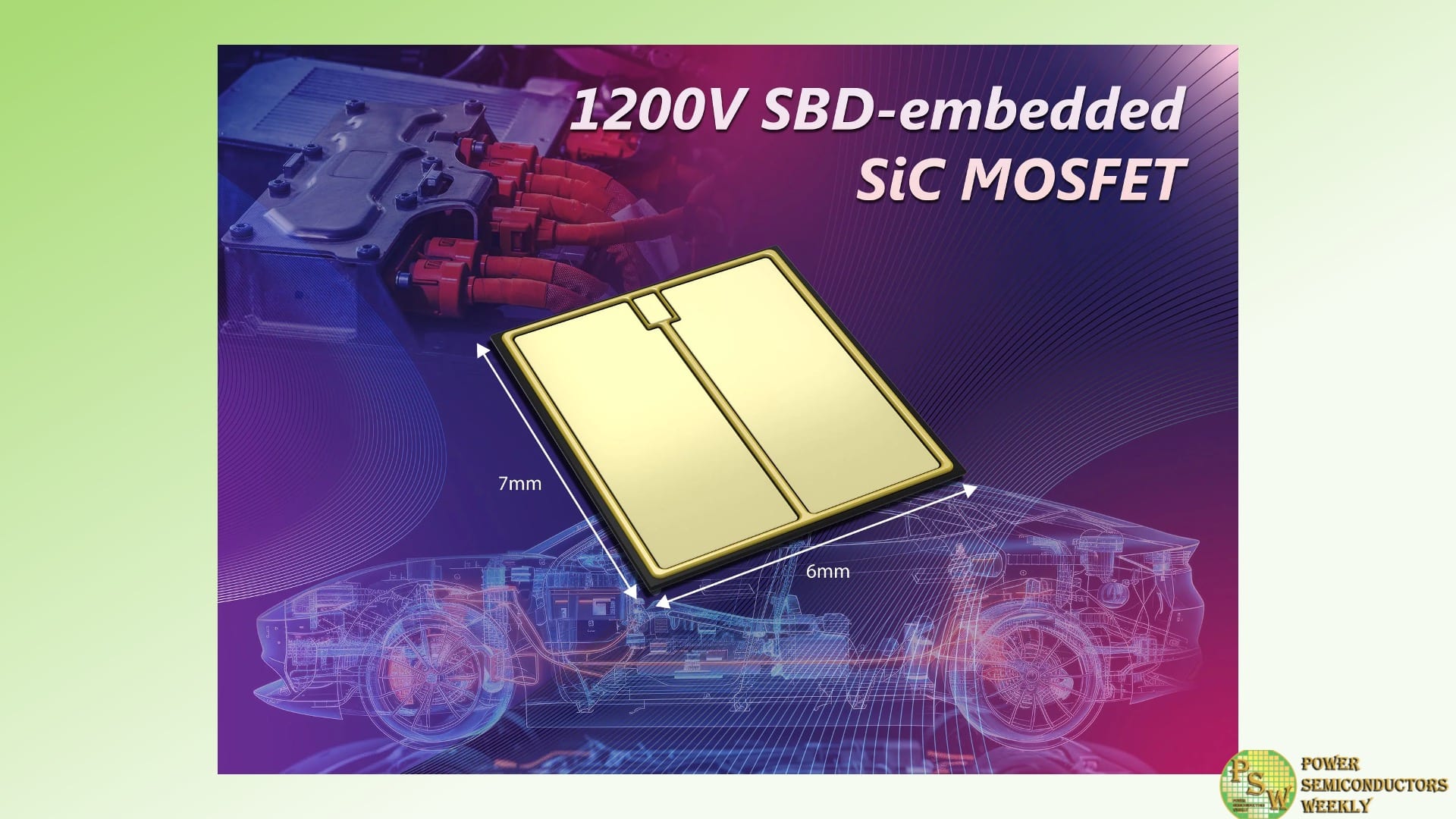
Toshiba Electronics Europe GmbH has developed new 1200V silicon carbide (SiC) MOSFETs with low on-resistance (RDS(ON)) and high levels of reliability. The devices are particularly suited to applications within automotive traction inverters. They are now available and shipping as early test samples in bare die format – allowing customers to customise them to meet the needs of their applications.
The new X5M007E120 uses a manufacturing process that reduces on-resistance per unit area by up to 30%. Unlike existing methods that utilise a striped-pattern construction, the new devices arrange the embedded Schottky barrier diodes (SBDs) in a check-pattern to achieve lower on-resistance.
Many SiC MOSFETs increase on-resistance as body diodes are energised during reverse conduction, which can lead to reliability issues. Toshiba SiC MOSFETs alleviate this issue by preventing body diodes from operating as SBDs are embedded into the MOSFETs. This approach maintains the reduction in on-resistance while ensuring reliability during reverse conduction.
With electric motors consuming over 40% of the world’s electrical energy, efficient operation is essential to sustainability. The re-arrangement of SBDs in this device has suppressed body diode energisation, and the upper limit of unipolar operation has increased to around double without increasing the SBD mounting area. Additionally, channel density is improved. These enhancements contribute to energy efficiency in applications, including motor control inverters.
Reducing RDS(ON) within a SiC MOSFET can cause excess current flow during short-circuit operations. By adopting a deep barrier structure, the X5M007E120 reduces excessive current within the MOSFET section and leakage current in the SBDs section during short-circuit operation. This enables durability during short-circuit conditions while maintaining high levels of reliability against reverse conduction operation.
The new X5M007E120 has a VDSS of 1200V and is rated for a drain current (ID) of 229A continuously, with 458A for pulsed operation (ID Pulse). RDS(ON) is as low as 7.2mΩ, and the device can operate with channel temperatures (Tch) as high as 175°C. The devices are AEC-Q100 qualified for automotive applications.
Engineering samples of the new X5M007E120 are expected to ship during 2025, with mass production samples scheduled to start in 2026.
Toshiba will continue to seek ways to further improve the characteristics of its products. The company will contribute to realising a decarbonised society by providing customers with power semiconductors for applications where energy efficiency is essential, such as inverters for motor control and power control systems for electrical vehicles.
Original – Toshiba
-
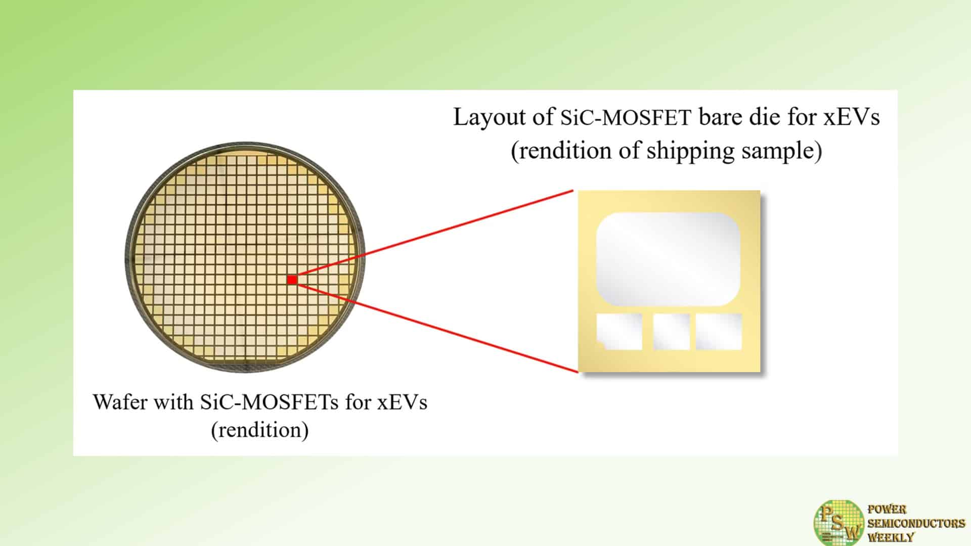
Mitsubishi Electric Corporation announced that it will begin shipping samples of a silicon carbide (SiC) metal-oxide-semiconductor field-effect transistor (MOSFET) bare die for use in drive-motor inverters of electric vehicles (EVs), plug-in hybrid vehicles (PHEVs) and other electric vehicles (xEVs) on November 14.
Mitsubishi Electric’s first standard-specification SiC-MOSFET power semiconductor chip will enable the company to respond to the diversification of inverters for xEVs and contribute to the growing popularity of these vehicles. The new SiC-MOSFET bare die for xEVs combines a proprietary chip structure and manufacturing technologies to contribute to decarbonization by enhancing inverter performance, extending driving range and improving energy efficiency in xEVs.
Mitsubishi Electric’s new power semiconductor chip is a proprietary trench SiC-MOSFET that reduces power loss by about 50% compared to conventional planar SiC-MOSFETs. Thanks to proprietary manufacturing technologies, such as a gate oxide film process that suppresses fluctuations in power loss and on-resistance, the new chip achieves long-term stability to contribute to inverter durability and xEV performance.
Original – Mitsubishi Electric
-
Littelfuse, Inc. announced the release of the IXTN400N20X4 and IXTN500N20X4 Ultra Junction X4-Class Power MOSFETs.
The new devices expand upon the current 200 V X4-Class Ultra Junction MOSFETs, featuring some of the lowest on-state resistances available. The high current ratings of these MOSFETs allow designers to replace multiple low-current rated devices connected in parallel, streamlining the design process and enhancing both reliability and power density in applications. Additionally, the screw-mounted terminals of the SOT-227B package enable rugged and stable mounting.
These new 200 V MOSFETs deliver the lowest on-state resistances, enhancing and complementing the existing Littelfuse X4-Class Ultra Junction family portfolio. Compared to the existing state-of-the-art X4-Class MOSFET solutions, these MOSFETs offer up to ~2x higher current ratings and RDS(on) values up to ~63% lower.
The new MOSFETs are ideal for a range of low-voltage power applications where minimizing on-state losses is essential, including:
- Battery Energy Storage Systems (BESS),
- Battery chargers,
- Battery formation,
- DC/battery load switch, and
- Power supplies.
“The new devices will allow designers to replace multiple low-current rated devices, connected in parallel, with a single device solution,” said Sachin Shridhar Paradkar, Global Product Marketing Engineer at Littelfuse. “This unique solution simplifies gate driver design, improves reliability, improves power density and PCB space utilization.”
The Ultra Junction X4-Class Power MOSFET offers the following key performance benefits:
- Low conduction losses
- Minimized parallel connection effort
- Simplified driver design with minimal driver losses
- Simplified thermal design
- Increased power density
A MOSFET with low on-state resistance (RDS(on)) is the ideal choice in applications where minimal on-state losses are crucial. It significantly reduces the power dissipation during operation, leading to lower conduction losses, higher efficiency, and less heat generation. This makes it perfect for power-sensitive applications such as power supplies, motor drivers, and battery-operated devices where maintaining high efficiency and thermal management is crucial.
Performance Specifications
Performance Specs IXTN500N20X4 IXTN400N20X4 Package Aluminum-nitride ceramic-based isolated SOT-227B On-state resistance RDS(on) = 1.99 mΩ @ Tvj = 25°C RDS(on) = 3 mΩ @ Tvj = 25°C High nominal current rating 500 A @ TC = 25°C 340 A @ TC = 25°C Gate charge Qg = 535 nC Qg = 348 nC Thermal resistance RthJC = 0.13 K/W RthJC = 0.18 K/W Original – Littelfuse
-

MCC Semi announced the latest innovation in their MOSFET lineup. The 100V wide SOA MCTL2D0N10YHR with split-gate trench technology satisfies the design demands of high-performance applications with ease. Balancing efficiency and reliability in harsh conditions is no longer an issue, thanks to this N-channel power MOSFET’s wide safe operating area (SOA) and a host of efficient characteristics.
This SOA comparison highlights significant differences in drain current between two 100V MOSFETs, MCTL300N10YB and MCTL2D0N10YHR, at 10ms pulse. This MOSFET’s wide SOA enhances safety and performance while overcoming common challenges engineers face when designing for high-power applications. It also provides a host of features that add up to ultimate efficiency and reliability. With a gate charge and on-resistance of 2mΩ, this MOSFET also optimizes energy use at every angle, reducing operational costs.
Designed to withstand junction temperatures of up to 175⁰C, this component delivers unquestionable performance in environments where lesser components would fail. Excellent thermal management is also assured, thanks to the TOLL package engineered for superior heat dissipation, which mitigates thermal-related issues. MCC’s 100V MOSFET is the ideal solution for diverse applications, including telecommunications, computing, audio amplification, and motor controls.
Features & Benefits:
- Wide SOA: Ensures safe operation across a broad range of conditions.
- Split-gate Trench (SGT) Technology: Provides enhanced performance and efficiency.
- Low On-Resistance: Maximizes efficiency by minimizing power losses.
- Low Conduction Losses: Reduces heat generation during operation.
- Low Gate Charge: Maximizes efficiency by minimizing switching losses.
- Low Gate Charge: Maximizes efficiency by minimizing switching losses.
- Excellent Thermal Performance: TOLL package facilitates superior heat dissipation.
Original – Micro Commercial Components
-

Vishay Intertechnology, Inc. introduced two new IGBT and MOSFET drivers in the compact, high isolation stretched SO-6 package. Delivering high peak output currents of 3 A and 4 A, respectively, the Vishay Semiconductors VOFD341A and VOFD343A offer high operating temperatures to +125 °C and low propagation delay of 200 ns maximum.
Consisting of an AlGaAs LED optically coupled to an integrated circuit with a power output stage, the optocouplers are intended for solar inverters and microinverters; AC and brushless DC industrial motor control inverters; and inverter stages for AC/DC conversion in UPS. The devices are ideally suited for directly driving IGBTs with ratings up to 1200 V / 100 A.
The high operating temperature of the VOFD341A and VOFD343A provides a higher temperature safety margin for more compact designs, while their high peak output current allows for faster switching by eliminating the need for an additional driver stage. The devices’ low propagation delay minimizes switching losses, while facilitating more precise PWM regulation.
The optocouplers’ high isolation package enables high working voltages up to 1.140 V, which allows for high voltage inverter stages, while still maintaining enough voltage safety margin. The RoHS-compliant devices offer high noise immunity of 50 kV/µs, which prevents fail functions in fast switching power stages.
Original – Vishay Intertechnology
-

Toshiba Electronic Devices & Storage Corporation has expanded the lineup of 150V N-channel power MOSFETs with new six products that use the new generation process “U-MOSⅩ-H series.” Products in this series are suitable for the switching power supplies of industrial equipment such as data centers and communication base. The package of new products is a three-pin through hole type: TO-220 for “TK4R9E15Q5, TK7R2E15Q5 and TK9R6E15Q5” and TO-220SIS for “TK5R0A15Q5, TK7R4A15Q5 and TK9R7A15Q5.”
The new products use the U-MOSⅩ-H process to achieve low drain-source On-resistance. In particular, TK4R9E15Q5 features the excellent low drain-source On-resistance of 4.9mΩ (max). In addition, the new products uses high-speed diode (HSD) to improve reverse recovery characteristics, which are important for synchronous rectification applications, by reducing reverse recovery charge and faster reverse recovery time. Used in synchronous rectification applications, the new products reduce the power loss of switching power supplies and help improve efficiency.
The first product TPH9R00CQ5 which uses HSD, has approximately 74% less reverse recovery charge and approximately 44% faster reverse recovery time than Toshiba‘s existing product TPH9R00CQH, which does not use HSD. The U-MOSⅩ-H process using this HSD has applied to through hole type packages in addition to surface mount type packages.
The new products have reduced the drain source spike voltage generated between the drain and source when MOSFET is switching, helping to lower EMI in switching power supplies.
Toshiba will continue to promote the expansion of its power MOSFET lineup, which helps improve the efficiency of power supplies, thereby contributing to reducing the power consumption of equipment.
Applications
- Switching power supplies for communication equipment, etc. (high efficiency AC-DC converters, high efficiency DC-DC converters, etc.)
- Motor control equipment (motor drives, etc.)
Features
- Excellent low On-resistance:
TK4R9E15Q5 RDS(ON)=4.9mΩ (max) (VGS=10V) - Low reverse recovery charge:
TK9R6E15Q5 Qrr=32nC (typ.) (-dIDR/dt=100A/μs) - Fast reverse recovery time:
TK9R6E15Q5 trr=40ns (typ.) (-dIDR/dt=100A/μs)
Original – Toshiba
