-
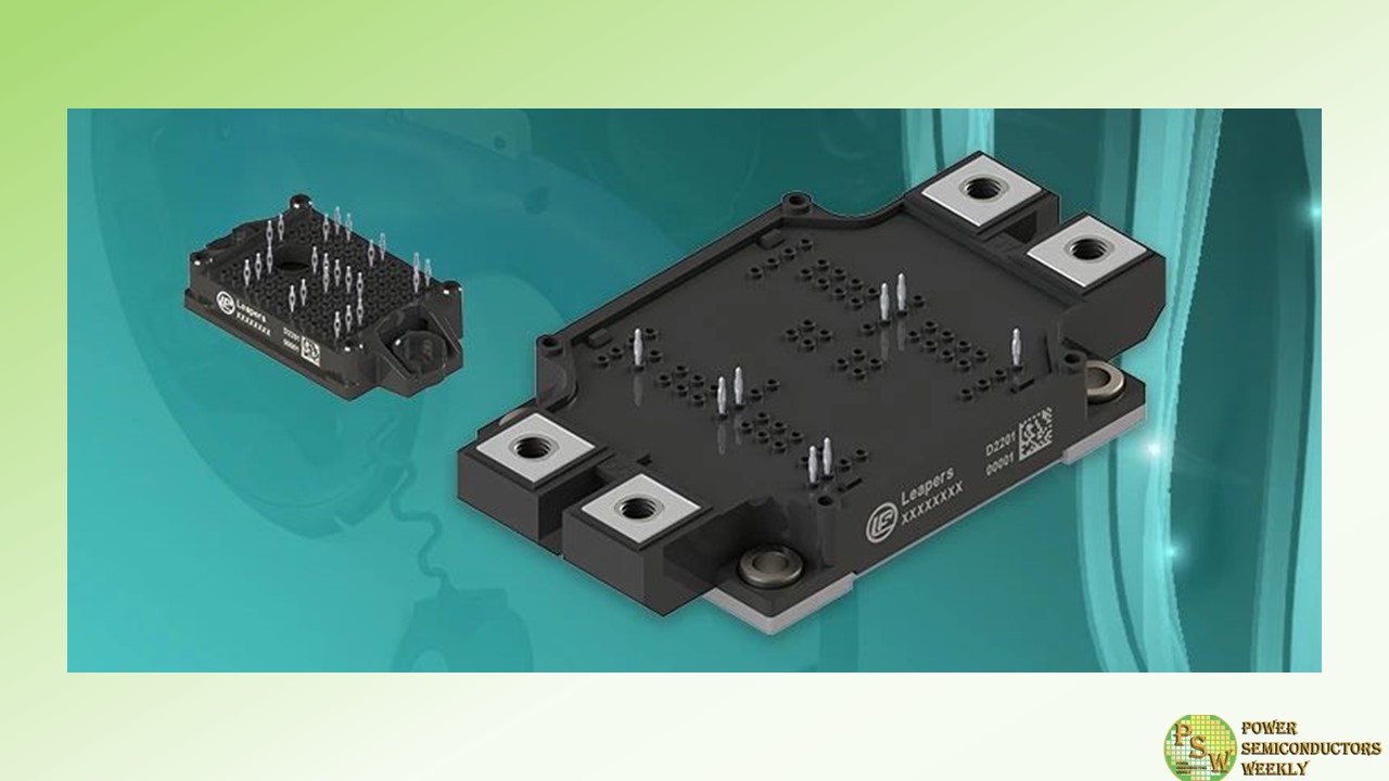
Today some applications tend to increase bus voltage, and using 1200V SiC power modules can no longer correspond to voltage requirements. Using 1700V SiC devices can solve the problem, but it comes with a price.
Leapers Semiconductor announced a new series of 1400V SiC power modules in already familiar E0 and ED3S packages. They are the perfect solution to the mentioned problem, providing great performance at affordable price.
At the moment the new series 1400V SiC modules come in Half-Bridge, H-Bridge, and Boost topologies.
Leapers Semiconductor new SiC product family features:
– 1,4kV voltage
– 50 – 600A current
– 3,2 – 40 mOhm Rds(on)
– Epoxy resin
– Si3N4 AMB substrate
– Low thermal resistance
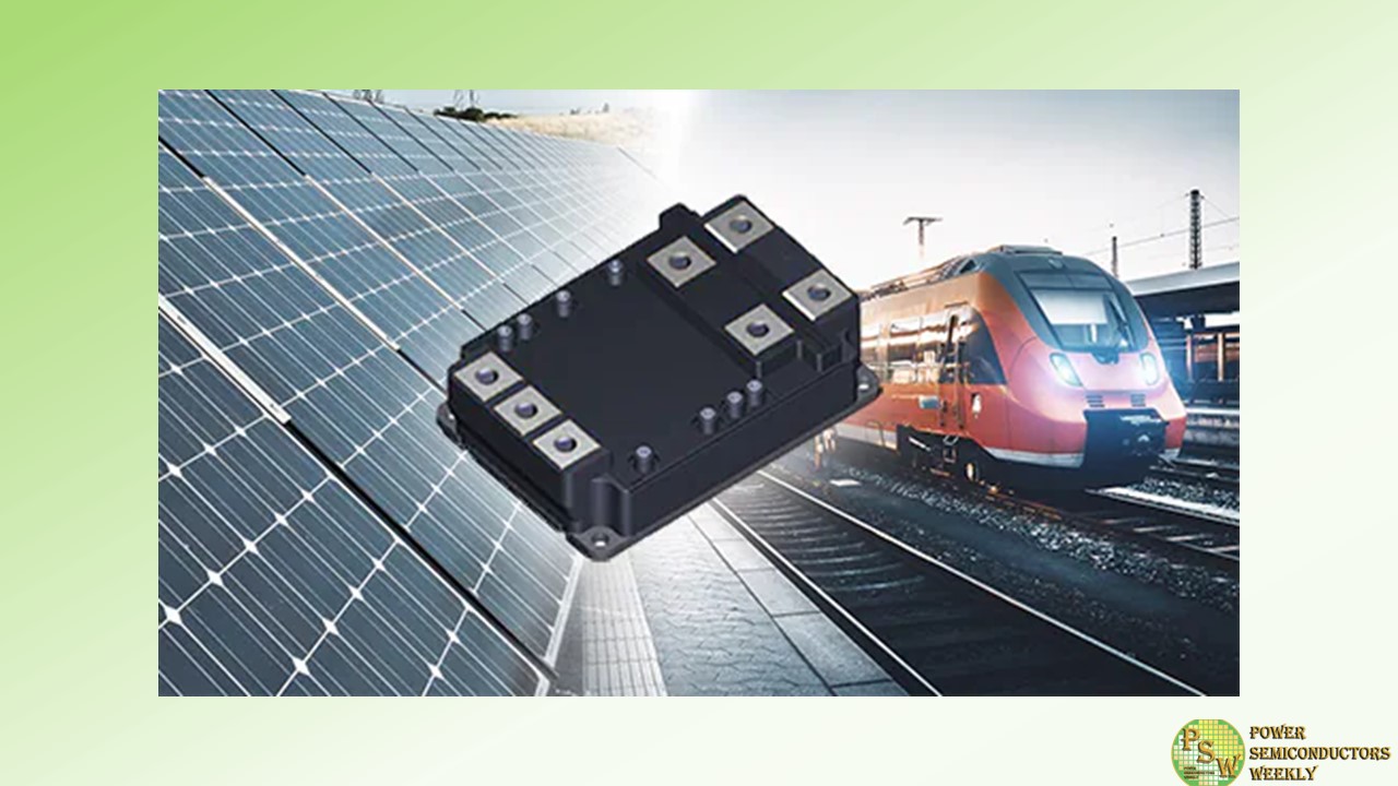
– Low switching lossesFirst batches of 1400V SiC power modules successfully passed field tests by the end customers and soon will be mass used in:
– DC fast chargers
– Commercial EVs
– Power supplies for production of hydrogen
– DC/DC convertersOriginal – Leapers Semiconductor
-
Toshiba Electronic Devices & Storage Corporation has launched chopper SiC MOSFET modules “MG800FXF1ZMS3” and ”MG800FZF1JMS3” with ratings of 3300 V and 800 A using 3rd generation silicon carbide (SiC) MOSFET and SBD chips for industrial equipment and has expanded its lineup.
The new products MG800FXF1ZMS3 and MG800FXF1JMS3 adopt an iXPLV package with Ag sintering internal bonding technology and high compatibility with mounting. These offers low conduction loss with low drain-source on-voltage (sense) of 1.3 V (typ.), and also offers low switching loss with low turn-on switching loss of 230 mJ (typ.) and low turn-off switching loss of 230 mJ (typ.). These contribute to reducing the power loss of equipment and the size of cooling device.
The lineup of Toshiba’s MOSFET modules of iXPLV package has three products, including existing product MG800FXF2YMS3 (3300 V / 800 A / Dual SiC MOSFET module.) This provides a wide range of product selection. This can be used in 2-level inverters, buck/boost converters and 3-level inverters.
Toshiba will continue to meet the market needs for high efficiency and the downsizing of industrial equipment.
Applications
Industrial equipment
- Inverters and converters for railway vehicles
- Renewable energy power generation systems
- Motor control equipment for industrial equipment, etc.
Features
- Low drain-source on-voltage (sense):
VDS(on)sense=1.3 V (typ.) (ID=800 A, VGS=+20 V, Tch=25 °C) - Low turn-on switching loss:
Eon=230 mJ (typ.) (VDD=1800 V, ID=800 A, Tch=175 °C) - Low turn-off switching loss:
Eoff=230 mJ (typ.) (VDD=1800 V, ID=800 A, Tch=175 °C)
Original – Toshiba
-
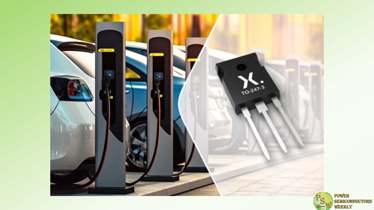
Nexperia announced its first silicon carbide (SiC) MOSFETs with the release of two 1200 V discrete devices in 3-pin TO-247 packaging with RDS(on) values of 40 mΩ and 80 mΩ. NSF040120L3A0 and NSF080120L3A0 are the first in a series of planned releases which will see Nexperia’s SiC MOSFET portfolio quickly expand to include devices with a variety of RDS(on) values in a choice of through-hole and surface mounted packages.
This release addresses the market demand for the increased availability of high performance SiC MOSFETs in industrial applications including electric vehicle (EV) charging piles, uninterruptible power supplies (UPS) and inverters for solar and energy storage systems (ESS).
“With these inaugural products, Nexperia and Mitsubishi Electric wanted to bring true innovation to a market that has been crying out for more wide-bandgap device suppliers”, according to Katrin Feurle, Senior Director & Head of Product Group SiC at Nexperia. “Nexperia can now offer SiC MOSFET devices which offer best-in-class performance across several parameters, including high RDS(on) temperature stability, low body diode voltage drop, tight threshold voltage specification as well as a very well-balanced gate charge ratio making the device safe against parasitic turn on. This is the opening chapter in our commitment to producing the highest quality SiC MOSFETs in our partnership with Mitsubishi Electric. Together we will undoubtedly push the boundaries of SiC device performance over the coming years”.
“Together with Nexperia, we’re thrilled to introduce these new SiC MOSFETs as the first product of our partnership”, says Toru Iwagami, Senior General Manger, Power Device Works, Semiconductor & Device Group in Mitsubishi Electric. “Mitsubishi Electric has accumulated superior expertise of SiC power semiconductors, and our devices deliver a unique balance of characteristics.”RDS(on) is a critical performance parameter for SiC MOSFETs as it impacts conduction power losses. Nexperia identified this as a limiting factor in the performance of many currently available SiC devices and used its innovative process technology to ensure its new SiC MOSFETs offer industry-leading temperature stability, with the nominal value of RDS(on) increasing by only 38% over an operating temperature range from 25°C to 175°C. Unlike other many currently available SiC devices in the market.
Nexperia’s SiC MOSFETs also exhibit the very low total gate charge (QG), which brings the advantage of lower gate drive losses. Furthermore, Nexperia balanced gate charge to have an exceptionally low ratio of QGD to QGS, a characteristic which increases device immunity against parasitic turn-on.
Together with the positive temperature coefficient of SiC MOSFETs, Nexperia’s SiC MOSFETs offers also ultra-low spread in device-to device threshold voltage, VGS(th), which allows very well-balanced current-carrying performance under static and dynamic conditions when devices are operated in parallel. Furthermore, low body diode forward voltage (VSD) is a parameter which increases device robustness and efficiency, while also relaxing the dead-time requirement for asynchronous rectification and free wheel operation.
Nexperia is also planning the future release of automotive grade MOSFETs. The NSF040120L3A0 and NSF080120L3A0 are available in production quantities now. Please contact Nexperia sales representatives for samples of the full SiC MOSFET offering.
Original – Nexperia
-
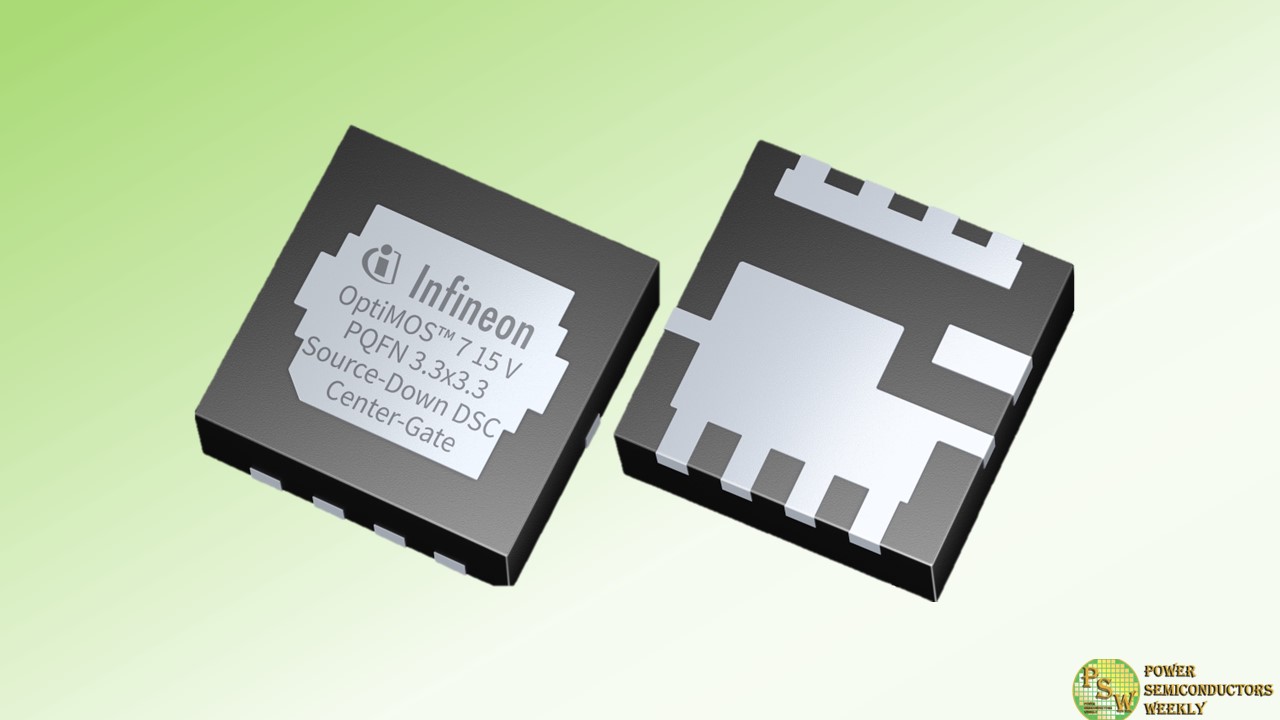
The ever-increasing power demand in data centers and computing applications requires advancements in power efficiency and compact power supply design. Infineon Technologies AG responds to trends on the system level by introducing its new OptiMOS™ 7 family, industry’s first 15 V trench power MOSFET technology. The OptiMOS 7 15 V series primarily targets optimized DC-DC conversion for servers, computing, datacenter, and artificial intelligence applications.
The product portfolio includes the latest PQFN 3.3 x 3.3 mm² Source-Down, with bottom- and dual-side cooling variants in standard- and center-gate footprints. The portfolio also includes a robust PQFN 2 x 2 mm² variant with a reinforced clip. The OptiMOS 7 15 V technology is specifically tailored for DC-DC conversions with low output voltages, particularly in server and computing environments. This advancement aligns with emerging shifts towards high ratio DC-DC conversion in data-center power distribution.
Compared to the established OptiMOS5 25 V, the new OptiMOS 7 15 V achieves a reduction of R DS(on) and FOMQ g by ~30 percent, and FOMQ OSS by ~50 percent by lowering the breakdown voltage. The PQFN 3.3 x 3.3 mm² Source-Down package variants provide a more versatile and effective PCB-design. Furthermore, the PQFN 2 x 2 mm² package provides a pulsed current capability higher than 500 A and a typical R thJC of 1.6 K/W.
By minimizing conduction and switching losses and incorporating advanced packaging technology, thermal management becomes easy and effective, setting new benchmarks both for power density and overall efficiency.
Original – Infineon Technologies
-
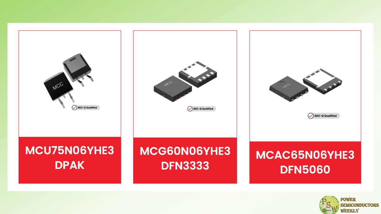
MCC Semi expanded its growing auto-grade portfolio with three new 60V N-channel MOSFETs: MCU75N06YHE3-TP, MCG60N06YHE3-TP, and MCAC65N06YHE3-TP.
Leveraging split-gate trench (SGT) MOSFET technology, MCC’s new products deliver optimal performance, efficiency, and thermal management, making them the intelligent choice for a range of demanding auto applications.
With on-resistance as low as 4.8mΩ, these AEC-Q101 qualified MOSFETs guarantee optimal power flow while significantly reducing power losses.
DFN333, DFN5060, and DPAK package options enable design flexibility and compatibility with various automotive systems.
Original – Micro Commercial Components
-
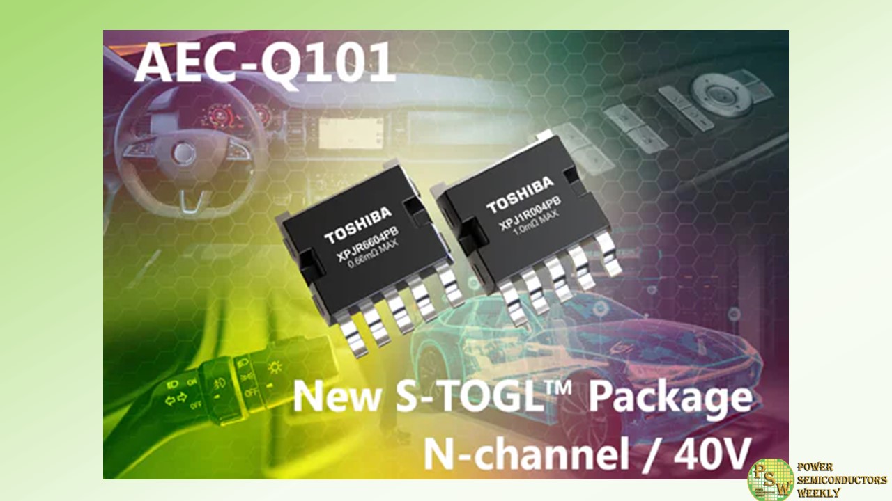
Toshiba Electronics Europe GmbH has launched a pair of automotive grade 40V N-channel power MOSFETs based upon their latest U-MOS IX-H process. The new devices use a new S-TOGLTM (Small Transistor Outline Gull-wing Leads) package that offers a number of advantages in automotive applications.
Automotive safety-critical applications such as steering, braking and autonomous driving systems generally require more devices than other systems to meet redundancy requirements. Here, a power MOSFET with high current density is required due to the size constraints within automotive equipment.
The new XPJR6604PB and XPJ1R004PB have a VDSS rating of 40V and the XPJR6604PB is rated for a continuous drain current (ID) of 200A (XPJ1R004PB = 160A). Both devices are rated for pulsed current (IDP) at 3x this value, 600A and 480A respectively. The 200A rating is higher than that achieved by Toshiba’s 6.5mm × 9.5mm DPAK+ package.
The new XPJR6604PB and XPJ1R004PB automotive MOSFETs use Toshiba’s innovative new S-TOGLTM package that measures just 7.0mm × 8.44mm × 2.3mm. The products are post-less and feature a multi-pin structure for the source leads that significantly decreases package resistance.
Combining the S-TOGLTM package with Toshiba’s U-MOS IX-H process gives the XPJR6604PB an on-resistance (RDS(ON) Compared to this device, the mounting area has reduced by around 55% compared while retaining the channel-to-case thermal resistance characteristics (Zth(ch-c)) – XPJR6604PB = 0.4ºC/W and XPJ1R004PB = 0.67ºC/W.
Many automotive applications are based in severely harsh environments, so the reliability of surface mount solder joints is a critical consideration. Toshiba’s S-TOGLTM package uses gull-wing leads that reduce mounting stress, improving the reliability of the solder joint.
Suited to harsh temperature environments, the MOSFETs are AEC-Q101 qualified and capable of operating at channel temperatures (Tch) as high as 175ºC.
Toshiba offers matched shipments for the devices, in which the gate threshold voltage range does not exceed 0.4V for each reel. This facilitates designs with small characteristic variations for applications requiring parallel connectivity for high-current operation.
Original – Toshiba
-
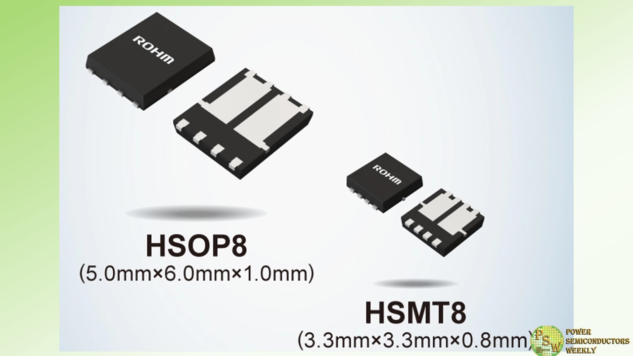
ROHM has developed dual MOSFETs that integrate two 100V chips in a single package – ideal for fan motor drive applied in communication base stations and industrial equipment. New five-models have been added as part of the HP8KEx/HT8KEx (Nch+Nch) and HP8MEx (Nch+Pch) series.
Recent years have seen a transition to higher voltages from conventional 12V/24V to 48V systems in communication base stations and industrial equipment, – intending to achieve higher efficiency by reducing current values. In these situations, switching MOSFETs are required a withstand voltage of 100V to account for voltage fluctuations, as 48V power supplies are also used in the fan motors for cooling these applications.
However, increasing the breakdown voltage raises ON resistance (RDS(on)) (which is in a trade-off relationship), leading to decreased efficiency, making it difficult to achieve both lower RDS(on) and higher breakdown voltage. Moreover, unlike multiple individual drive MOSFETs normally applied in fan motors - dual MOSFETs that integrate two chips in one package are increasingly being adopted to save space.
In response, ROHM developed two new series – the HP8KEx/HT8KEx (Nch+Nch) and the HP8MEx (Nch+Pch) – that combine Nch and Pch MOSFET chips using the latest processes. Both series achieve the industry’s lowest RDS(on) by adopting new backside heat dissipation packages with excellent heat dissipation characteristics. As a result, RDS(on) is reduced by up to 56% compared with standard dual MOSFETs (19.6mΩ for the HSOP8 and 57.0mΩ for the HSMT8 Nch+Nch), contributing to significantly lower set power consumption.
At the same time, combining two chips in a single package provides greater space savings by reducing area considerably. For example, replacing two single-chip TO-252 MOSFETs with one HSOP8 decreases footprint by 77%.
Next, ROHM will continue to expand its dual MOSFET lineup to withstand voltages ideal for industrial equipment while also developing low-noise variants. This is expected to contribute to solving social issues such as environmental protection by saving space and reducing power consumption in various applications.
Application Examples
– Fan motors for communication base stations
– Fan motors for factory automation, and other industrial equipment
– Fan motors for data center servers, etc.Original – ROHM
-
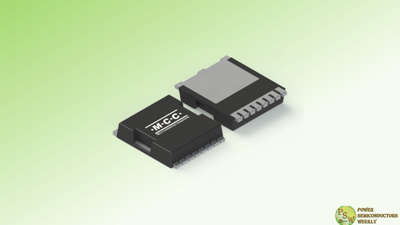
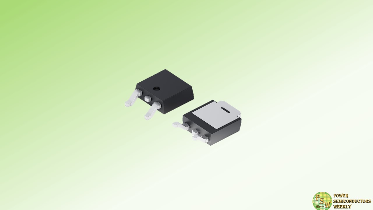
Micro Commercial Components introduced the latest auto-grade MOSFET in the TOLL package for today’s demanding e-mobility applications. AEC-Q101 qualified and ready to empower auto designs, MCC’s100V MCTL300N10YHE3 MOSFET delivers exceptional performance and unmatched reliability for a range of systems, including battery management systems, motor drives, and interior or exterior LED lighting.
Designed with split-gate trench (SGT) technology, this component features low on-resistance and high current density to maximize efficiency while handling power loads. It’s also a great replacement for traditional MOSFETs due to its enhanced performance. The innovative TOLL-8 package provides design flexibility due to its compact footprint and optimal heat dissipation to ensure safe operation in high-temperature environments.
Fully RoHS compliant, MCTL300N10YHE3 is the ideal solution for automotive applications.
Features & Benefits:
- Exceptional performance and reliability
- AEC-Q101 qualified
- SGT technology for improved performance
- Low on-resistance for enhanced efficiency
- High current density capabilities
- Low-profile TOLL package saves design space
- Excellent heat dissipation for reliable operation in high temperatures
- Halogen-free and lead-free finish for environmental friendliness and compliance with RoHS regulations
Original – Micro Commercial Components
-
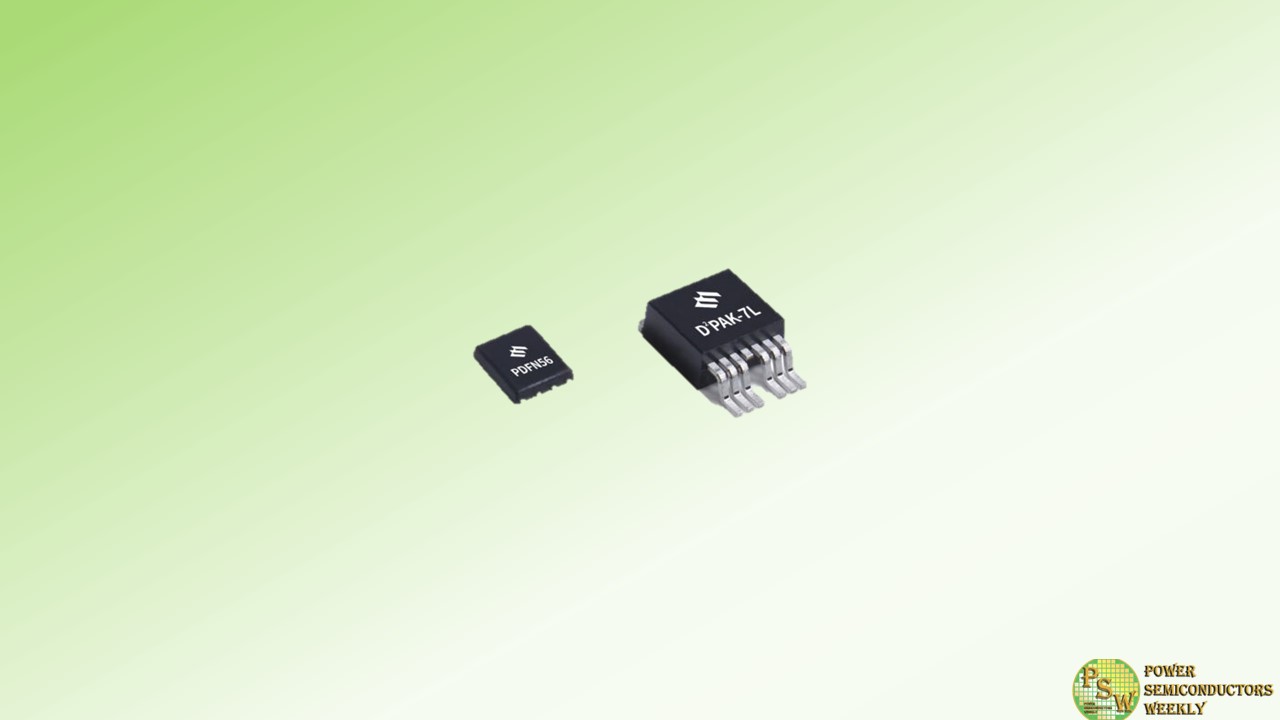
Magnachip Semiconductor Corporation announced the launch of two new 150V MXT MV Metal-Oxide-Semiconductor Field-Effect Transistors (MOSFETs), using its 8th-generation trench MOSFET technology.
Energy efficiency is crucial in high-power devices for reducing power consumption and ensuring stability. These newly released 8th-generation 150V MXT MV MOSFETs (MDES15N056PTRH, MDU150N113PTVRH) were developed by leveraging Magnachip’s cutting-edge trench MOSFET technology. In particular, the RDS(on) (the resistance value between the drain and the source of MOSFETs during on-state operation) of MDES15N056PTRH was reduced by 22% compared to the previous generation, thereby significantly enhancing energy efficiency in applications.
By improving the core cell and termination design, the Figure of Merit (FOM: RDS(on) x Qg) of MDES15N056PTRH and MDU150N113PTVRH has been improved by 23% and 39%, respectively, compared to the previous version. Furthermore, the adoption of surface-mount type packages, such as D2PAK-7L (TO-263-7L) and PDFN56, reduces MOSFET sizes, enabling flexible design of various applications, such as motor controllers, battery management systems (BMSs), residential solar inverters and industrial power supplies.
“Following the introduction of five 8th-generation 200V and 150V MOSFETs last year, we are pleased to now release two additional 150V MXT MV MOSFET product offerings in new packages,” said YJ Kim, CEO of Magnachip. “Magnachip will continue to expand its high-efficiency MXT MOSFET product portfolio, including new releases based on 180nm microfabrication technology in the near future.”
Original – Magnachip Semiconductor
-
Littelfuse, Inc. announced the release of IXTY2P50PA, the first automotive-grade PolarP™ P-Channel Power MOSFET. This innovative product design meets the demanding requirements of automotive applications, providing exceptional performance and reliability.
The key differentiator of the –500 V, –2 A IXTY2P50PA is its AEC-Q101 qualification, making it ideal for automotive applications. This qualification ensures that the MOSFET meets the automotive industry’s stringent quality and reliability standards. With this qualification, automotive manufacturers can trust that the IXTY2P50PA will deliver exceptional application performance and reliability.
One of the standout features is its low conduction loss. With a maximum on-state resistance of 4.2 Ω, this P-Channel Power MOSFET offers reduced power dissipation, decreasing heat generation and improving efficiency in the end applications. Additionally, the MOSFET provides excellent switching performance, with a low gate charge of 11.9 nC, allowing for fast and efficient operation.
Another key advantage is its ruggedness in demanding operating environments and applications. With its dynamic dv/dt and avalanche rating, this MOSFET can withstand harsh conditions and deliver reliable performance. This combination makes it an excellent choice for automotive applications that require durability and reliability.
Furthermore, the IXTY2P50PA high-voltage automotive P-channel MOSFET enables a power-dense PCB design, thanks to its miniature TO-252 (DPAK) footprint in surface mount form factor. This compact footprint results in significant space savings on the PCB, allowing for more efficient and compact designs. Automotive manufacturers can benefit from this space-saving design, enabling them to optimize their applications and achieve greater functionality in limited space.
The PolarP Series is ideally suited for a range of automotive electronics and industrial applications, including:
- Automotive ECUs
- Automotive sensor circuits
- High-side switches
- Push-pull amplifiers
- Automatic test equipment
- Current regulators
Commenting on the launch of IXTY2P50PA, Raymon Zhou, Product Marketing Manager at Littelfuse, said, “We are thrilled to introduce the first automotive-grade PolarP P-Channel Power MOSFET to the market. The IXTY2P50PA offers exceptional performance and reliability, making it ideal for demanding automotive applications. With its AEC-Q101 qualification and competitive specifications, we believe this MOSFET will greatly benefit automotive manufacturers.”
Original – Littelfuse
