-
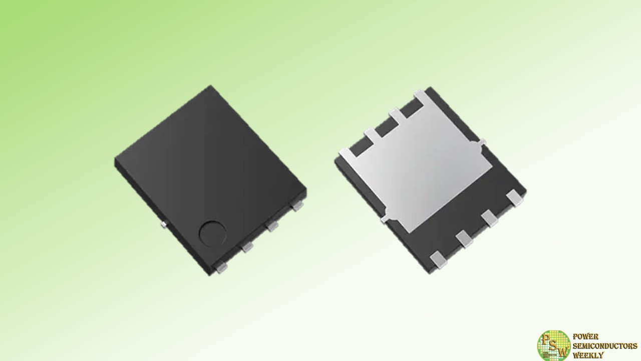
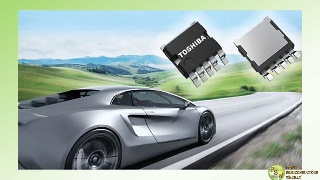
Toshiba Electronic Devices & Storage Corporation has started mass production of three 40 V N-channel MOSFETs using SOP Advance(WF) package for automotive and has expanded its lineup. The three models are “XPHR9904PS, XPH2R404PS and XPH3R304PS.”
The new products reduce drain-source On-resistance with the U-MOSIX process as with Toshiba’s precedence release products XPHR7904PS and XPH1R104PS. The drain-source On-resistance of XPH2R404PS is 2.4 mΩ (max), which is approximately 27 % lower than that of Toshiba’s existing product TPCA8083, and XPH3R304PS is 3.3 mΩ (max), which is approximately 42 % lower than that of Toshiba’s existing product TPCA8085.
The drain-source On-resistance of XPHR9904PS is 0.99 mΩ (max). Reducing drain-source On-resistance of these products contributes to low power consumption of automotive equipment. In addition, they are qualified with the automotive reliability standard AEC-Q101. The PPAP of IATF16949 is also available.
The package is a surface mount type SOP Advance(WF) that uses a wettable flank terminal structure, which facilitates automated visual inspection of the board mounting state.
Toshiba’s automotive MOSFETs support a variety of automotive applications and meet a wide range of customer needs.
Applications
- Automotive equipment: motor drives, switching power supplies, load switches, etc.
Features
- Low On-resistance
XPHR9904PS: RDS(ON)=0.99 mΩ (max) (VGS=10 V)
XPH2R404PS: RDS(ON)=2.4 mΩ (max) (VGS=10 V)
XPH3R304PS: RDS(ON)=3.3 mΩ (max) (VGS=10 V) - AEC-Q101 qualified
- PPAP of IATF16949 available
Original – Toshiba
-
Power semiconductors based on silicon carbide (SiC) offer several advantages, like high efficiency, power density, voltage resistance, and reliability. This creates opportunities for new applications and improved charging station technology innovations. Infineon Technologies announced a collaboration with Infypower, a Chinese market leader in new energy vehicle charging. Infineon will provide INFY with the industry-leading 1200 V CoolSiC™ MOSFET power semiconductor devices to improve the efficiency of electric vehicle charging stations.
“The collaboration between Infineon and Infypower in the field of charging solutions for electric vehicles (EV) provides an excellent system-level technology solution for the local EV charging station industry,” said Dr. Peter Wawer, Division President of Infineon’s Green Industrial Power Division. “It will significantly improve charging efficiency, accelerate charging speed, and create a better user experience for owners of electric cars.”
“With Infineon’s more than 20 years of continuous advancement in SiC product offering and the strength of integrated technology, Infypower can consolidate and maintain its technological outstanding position in the industry by adopting state-of-the-art product processes and design solutions“, said Qiu Tianquan, President of Infypower China. “We can also set a new standard for charging efficiency of DC chargers for new energy vehicles. As a result, customers can enjoy more convenience and unique value, promoting the healthy development of the EV charging industry.”
SiC’s high power density enables the development of high-performance, lightweight, and compact chargers, especially for supercharging stations and ultra-compact wall-mounted DC charging stations. Compared to traditional silicon-based solutions, SiC technology in EV charging stations can increase efficiency by 1 percent, reducing energy losses and operating costs. In a 100 kW charging station, this translates to 1 kWh of electricity savings, saving 270 Euros annually and reducing carbon emissions by 3.5 tons. This drives the increasing adoption of SiC power devices in EV charging modules.
As one of the first SiC power semiconductor manufacturers to use trench gate technology for transistors, Infineon has introduced an advanced design that provides high reliability for chargers. The devices offer a high threshold voltage and simplified gate driving . The CoolSiC MOSFET technology has been subjected to marathon stress tests and gate voltage jump stress tests before commercial release and regularly afterwards in form of monitoring to ensure highest gate reliability.
By integrating Infineon’s 1200 V CoolSiC MOSFETs, Infypower’s 30 kW DC charging module offers a wide constant power range, high power density, minimal electromagnetic radiation and interference, high protection performance and high reliability. In this way, it is well suited for the fast charging demand of most EVs while possessing a higher efficiency of 1 percent compared with other solutions on the market. Consequently, significant energy savings and carbon dioxide emission reduction are achieved, which are leading at a global level.
Original – Infineon Technologies
-

Aehr Test Systems announced it has received an initial customer order for a FOX-NP™ wafer level test and burn-in system, multiple WaferPak™ Contactors, and a FOX WaferPak Aligner to be used for engineering, qualification, and small lot production wafer level test and burn-in of their silicon carbide devices. The customer is a US-based multibillion-dollar semiconductor supplier serving several markets including automotive, computing, consumer, energy, industrial, and medical. The FOX-NP system, including the FOX WaferPak Aligner and initial WaferPaks are scheduled per the customer’s requested accelerated schedule to ship by the end of the calendar year 2023.
The FOX-NP system is configured with the new Bipolar Voltage Channel Module (BVCM) and Very High Voltage Channel Module (VHVCM) options that enable new advanced test and burn-in capabilities for silicon carbide power semiconductors using Aehr’s proprietary WaferPak full wafer Contactors. This new order highlights Aehr’s continued progression within the growing silicon carbide global power market.
Gayn Erickson, President and CEO of Aehr Test Systems, commented, “We are very excited that after conducting a detailed financial evaluation and multiple onsite visits to Aehr’s application lab, this new customer selected our FOX-P solution for engineering, qualification, and production of their silicon carbide power devices.
This evaluation included cost of ownership and system throughput, as well as device test, burn-in, and stabilization coverage. As their production capacity increases, they told us that they will quickly move to our FOX-XP multi-wafer test and burn-in systems for high-volume production. In addition to the automotive electric vehicle device opportunity, this customer in particular sees the enormous opportunity for silicon carbide power devices in industrial, solar, and other power applications.
“William Blair forecasts that in addition to the 4.5 million six-inch equivalent wafers that will be needed to meet the demand for electric vehicle related silicon carbide devices in 2030, another 2.8 million wafers are needed to address industrial, solar, electric trains, energy conversion and other applications in 2030. The interesting part of this is that most of these applications will be served with discrete MOSFETS in single die packages.
The cost of ownership of our solution proved to be more cost-effective and efficient for these devices than package part burn-in after the die are packaged in packages such as TO-247 or other discrete packages. This is a strong testimony of the advantage of wafer level burn-in as a better alternative to package part burn-in. This expands our silicon carbide test and burn-in market even more and this new customer helps expand Aehr’s presence in this market as our total addressable market (TAM) continues to grow.
“Aehr’s FOX-P systems and proprietary WaferPak full wafer Contactors enable our customers to do economical production volume test and reliability burn-in with processes such as High Temperature Gate Bias (HTGB) and High Temperature Reverse Bias (HTRB) very cost-effectively and ensure extremely high device quality. Our systems are typically used for long burn-in times lasting up to 24 hours or more.
We can do this for under $5.00 per hour per wafer capital depreciation cost while testing and burning-in up to several thousand devices at a time per wafer. This is also in a test system footprint that is up to 94% less than a typical test system on a standard semiconductor wafer prober, which in a precious clean room wafer facility is extremely important and saves a great deal of cost.
“The FOX family of compatible systems including the FOX-NP and FOX-XP multi-wafer test and burn-in systems and Aehr’s proprietary WaferPak full wafer contactors provide a uniquely cost-effective solution for burning in multiple wafers of devices at a single time to remove early life failures of silicon carbide devices, which is critical to meeting the initial quality and long-term reliability of the automotive, industrial, and electrification infrastructure industry needs.”
The FOX-XP and FOX-NP systems, available with multiple WaferPak Contactors (full wafer test) or multiple DiePakTM Carriers (singulated die/module test) configurations, are capable of functional test and burn-in/cycling of devices such as silicon carbide and gallium nitride power semiconductors, silicon photonics as well as other optical devices, 2D and 3D sensors, flash memories, magnetic sensors, microcontrollers, and other leading-edge ICs in either wafer form factor, before they are assembled into single or multi-die stacked packages, or in singulated die or module form factor.
Original – Aehr Test Systems
-

STMicroelectronics will supply BorgWarner Inc. with the latest third generation 750V silicon carbide (SiC) power MOSFETs dice for their proprietary Viper-based power module. This power module is used in BorgWarner’s traction inverter platforms for several current and future Volvo Cars electric vehicles.
“This collaboration will give Volvo Cars the opportunity to further increase the attractiveness of our electrical vehicles with longer range and faster charging. It will also support us on our journey towards being fully electric by 2030 and strengthen our increased vertical integration and our control of critical components,” says Javier Varela, Chief Operating Officer & Deputy CEO, Volvo Cars.
“BorgWarner is pleased to partner with ST to supply our longstanding customer Volvo Cars with inverters for their next generation of BEV platforms,” says Stefan Demmerle, Vice President of BorgWarner Inc. and President and General Manager, PowerDrive Systems.
To fully leverage the performance of ST’s SiC MOSFET dice, BorgWarner collaborated closely with ST’s technical team to match their die with BorgWarner’s Viper power switch, thereby maximizing inverter performance and delivering a compact and cost-effective architecture. The collaboration between the companies provides the high-volume capability that is required by the quickly growing EV market.
“Our collaboration with BorgWarner, a leading global automotive supplier in electrification, will enable Volvo Cars to offer their customers superior vehicle performance and range,” says Marco Monti, President, Automotive and Discrete Group, STMicroelectronics. “We are committed to expanding SiC capacity and to reinforcing our SiC supply, including through vertical integration, as we ramp up volumes to support our global automotive and industrial customers in their shift to electrification and higher efficiency.”
ST’s high-volume STPOWER SiC products are manufactured in its fabs in Italy, and Singapore, with advanced packaging and testing at its back-end facilities in Morocco and China. In October 2022, ST announced it would expand its wide bandgap manufacturing capacity with a new integrated SiC substrate manufacturing facility in Catania, home to the company’s power semiconductor expertise and the site of integrated research, development, and manufacturing of SiC.
Original – STMicroelectronics
-
Toshiba Electronic Devices & Storage Corporation has launched silicon carbide (SiC) MOSFETs, the “TWxxxZxxxC series,” that use a four-pin TO-247-4L(X) package that reduces switching loss with the company’s latest 3rd generation SiC MOSFETs chip for industrial equipment. Volume shipments of ten products, five with 650V ratings and five with 1200V, start today.
The new products are the first in Toshiba’s SiC MOSFET line-up to use the four-pin TO-247-4L(X) package, which allows Kelvin connection of the signal source terminal for the gate drive. The package can reduce the effect of source wire inductance inside the package, improving high-speed switching performance. For the new TW045Z120C, the turn-on loss is approximately 40% lower and the turn-off loss reduced by approximately 34%, compared with Toshiba’s current product TW045N120C in a three-pin TO-247 package. This helps to reduce equipment power loss.
Applications
- Switching power supplies (servers, data centers, communications equipment, etc.)
- EV charging stations
- Photovoltaic inverters
- Uninterruptible power supplies (UPS)
Features
- Four-pins TO-247-4L(X) package:
Switching loss is reduced by Kelvin connection of the signal source terminal for the gate drive - 3rd generation SiC MOSFETs
- Low drain-source On-resistance x gate-drain charge
- Low diode forward voltage: VDSF=-1.35V (typ.) (VGS=-5V)
Original – Toshiba
-
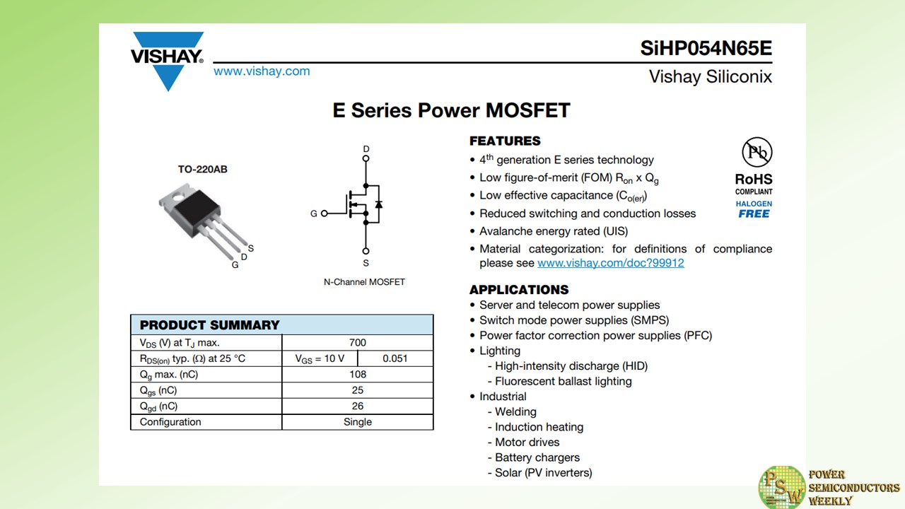
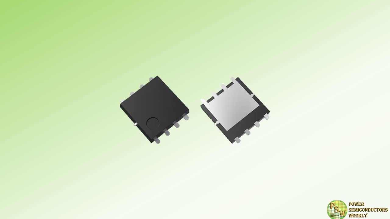
Vishay Intertechnology, Inc. introduced a new fourth-generation 650 V E Series power MOSFET that delivers high efficiency and power density for telecom, industrial, and computing applications. Compared to previous-generation devices, the Vishay Siliconix n-channel SiHP054N65E slashes on-resistance by 48.2 %, while offering a 59 % lower resistance times gate charge, a key figure of merit (FOM) for 650 V MOSFETs used in power conversion applications.
Vishay offers a broad line of MOSFET technologies that support all stages of the power conversion process, from high voltage inputs to the low voltage outputs required to power the latest high tech equipment. With the SiHP054N65E and other devices in the fourth-generation 650 V E Series family, the company is addressing the need for efficiency and power density improvements in two of the first stages of the power system architecture — power factor correction (PFC) and subsequent DC/DC converter blocks.
Typical applications will include servers, edge computing, and data storage; UPS; high intensity discharge (HID) lamps and fluorescent ballast lighting; solar inverters; welding equipment; induction heating; motor drives; and battery chargers.
Built on Vishay’s latest energy-efficient E Series superjunction technology, the SiHP054N65E’s low typical on-resistance of 0.051 Ω at 10 V results in a higher power rating for applications > 2 kW and allows the device to address the Open Compute Project’s Open Rack V3 (ORV3) standards. In addition, the MOSFET offers ultra low gate charge down to 72 nC. The resulting FOM of 3.67 Ω*nC is 1.1 % lower than the closest competing MOSFET in the same class, which translates into reduced conduction and switching losses to save energy and increase efficiency. This allows the device to address the specific titanium efficiency requirements in server power supplies or reach 96 % peak efficiency in telecom power supplies.
For improved switching performance in hard-switched topologies such as PFC, half-bridge, and two-switch forward designs, the MOSFET released today provides low typical effective output capacitances Co(er) and Co(tr) of 115 pF and 772 pF, respectively. The device’s resulting resistance times Co(er) FOM is an industry-low 5.87 Ω*pF. Offered in the TO-220AB package and providing increased dv/dt ruggedness, the SiHP054N65E is RoHS-compliant, halogen-free, and Vishay Green, and is designed to withstand overvoltage transients in avalanche mode with guaranteed limits through 100 % UIS testing.
Original – Vishay Intertechnology
-
Toshiba Electronic Devices & Storage Corporation has launched three 80 V N-channel power MOSFET products that use its latest generation process “U-MOSX-H series” and are suitable for switching power supplies for industrial equipment—used for such as data centers and communication base stations—and expanded the lineup.
The new products use the surface mount type SOP Advance(N) package, and their drain-source On-resistance (max) is 3 mΩ for “TPH3R008QM”, 6 mΩ for “TPH6R008QM”, and 8.8 mΩ for “TPH8R808QM”.
The new products have reduced the figure of merits (FOMs: expressed as On-resistance × charge characteristics.) In case of TPH3R008QM, it has reduced its FOMs, drain-source On-resistance × total gate charge by approximately 48 %, drain-source On-resistance × gate switch charge by approximately 16 %, and drain-source On-resistance × output charge by approximately 33 %, compared to Toshiba’s existing product TPH4R008NH. This contributes to lowering power consumption of equipment.
Toshiba is expanding its lineup of products to help cut equipment power consumption.
Applications
- Switching power supplies (high efficiency AC-DC converters, high efficiency DC-DC converters, etc.)
- Motor control equipment (motor drives, etc.)
Features
- Latest generation process U-MOSX-H series
- Low On-resistance:
TPH3R008QM RDS(ON)=3 mΩ (max) (VGS=10 V)
TPH6R008QM RDS(ON)=6 mΩ (max) (VGS=10 V)
TPH8R808QM RDS(ON)=8.8 mΩ (max) (VGS=10 V) - High channel temperature: Tch (max)=175 °C
Original – Toshiba
-
Toshiba Electronic Devices & Storage Corporation has launched two automotive 40V N-channel power MOSFETs, “XPJR6604PB” and “XPJ1R004PB,” that use Toshiba’s new S-TOGL™ (Small Transistor Outline Gull-wing Leads) package with U-MOS IX-H process chips. Volume shipments start today.
Safety-critical applications like autonomous driving systems ensure reliability through redundant design, with the result that they integrate more devices and require more mounting space than standard systems. Accordingly, advancing size reductions in automotive equipment requires power MOSFETs that can be mounted at high current densities.
XPJR6604PB and XPJ1R004PB use Toshiba’s new S-TOGL™ package (7.0mm×8.44mm) which features a post-less structure unifying the source connective part and outer leads. A multi-pin structure for the source leads decreases package resistance.
The combination of the S-TOGL™ package and Toshiba’s U-MOS IX-H process achieve a significant On-resistance reduction of 11% against Toshiba’s TO-220SM (W) package product, which has the same thermal resistance characteristics. The new package also cuts the required mounting area by approximately 55% against the TO-220SM(W) package.
On top of this, the 200A drain current rating of the new package is higher than Toshiba’s similarly sized DPAK + package (6.5mm×9.5mm), enabling high current flow. Overall, the S-TOGL™ package realizes high-density and compact layouts, reduces the size of automotive equipment, and contributes to high heat dissipation.
Since automotive equipment is used in extreme temperature environments, the reliability of surface mounting solder joints is a critical consideration. The S-TOGL™ package uses gull-wing leads that reduce mounting stress, improving the reliability of the solder joint.
Assuming that multiple devices will be connected in parallel for applications requiring higher-current operation, Toshiba supports grouping shipment for the new products, in which the gate threshold voltage is used for grouping. This allows designs using product groups with small characteristic variation.
Toshiba will continue to expand its product line-up of power semiconductor products and contribute to the realization of carbon neutrality with more user-friendly, high-performance power devices.
Features:
- New S-TOGL™ package: 7.0mm×8.44mm (typ.)
- Large drain current rating:
XPJR6604PB: ID=200A
XPJ1R004PB: ID=160A - AEC-Q101 qualified
- IATF 16949/PPAP available[4]
- Low On-resistance:
XPJR6604PB: RDS(ON)=0.53mΩ (typ.) (VGS=10V)
XPJ1R004PB: RDS(ON)=0.8mΩ (typ.) (VGS=10V)
Original – Toshiba
-
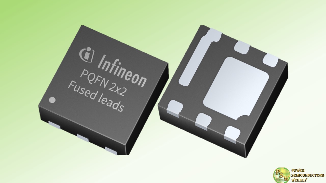
A small footprint of discrete power MOSFETs plays a critical role in achieving space savings, cost reduction, and easy-to-design applications. Additionally, higher power density can lead to layout routing flexibility and overall system size reduction. By expanding the current PQFN 2×2 portfolio with the new best-in-class OptiMOS™ power MOSFETs, Infineon Technologies AG offers benchmark solutions optimized for efficiency and performance in a small footprint. The new products are ideal for applications like synchronous rectification in switched mode power supplies (SMPS) for servers, telecom, and portable- and wireless chargers. Additional applications also include electric speed controllers for small brushless motors in drones.
The new OptiMOS 6 40 V and OptiMOS 5 25 V and 30 V power MOSFETs further optimize the proven OptiMOS technology for high-performance designs. They offer leading-edge silicon technology, package reliability, and superior thermal resistance (R thJC, max = 3.2 K/W) in the ultra-small PQFN 2×2 mm² package. The new devices combine industry-leading low on-resistance R DS(on) with industry-leading figures of merit (FOMs, Q G and Q OSS) for outstanding dynamic switching performance. As a result, MOSFETs with ultra-low switching and reduced conduction losses ensure optimal energy efficiency and power density, all while simplifying thermal management.
With the compact PQFN 2×2 mm² package outline, the OptiMOS power switches enable an improved system form factor with smaller, more flexible geometric outlines for end-user applications. The MOSFETs facilitate reliable system design with less need for paralleling, significantly reducing space and system cost.
Original – Infineon Technologies
-
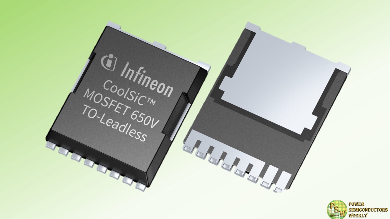
As digitalization, urbanization, and the rise of electro-mobility continue to shape the rapidly evolving world, the demand for power consumption is reaching unprecedented levels. Acknowledging energy efficiency as an important concern, Infineon Technologies AG addresses these megatrends with its silicon carbide (SiC) CoolSiC™ MOSFET 650 V in TO leadless (TOLL) packaging. The new SiC MOSFETs are enhancing Infineon’s comprehensive CoolSiC portfolio and are optimized for the lowest losses, the highest reliability, and ease-of-use in applications such as SMPS for servers, telecom infrastructure as well as energy storage systems and battery formation solutions.
The CoolSiC 650 V high-performance trench-based power SiC MOSFETs are offered in a very granular portfolio to best suit different target applications. The new family comes in a JEDEC-qualified TOLL package featuring a low parasitic inductance, allowing for higher switching frequency, reduced switching losses, good thermal management, and automated assembly. The compact form factor enables efficient and effective usage of the board space, empowering system designers to achieve exceptional power density.
The CoolSiC MOSFETs 650 V showcase remarkable reliability even in harsh environments, making them an ideal choice for topologies with repetitive hard commutation. The inclusion of the innovative .XT interconnect technology further enhances the devices’ thermal performance by reducing the thermal resistance (R th) and thermal impedance (Z th). In addition, the new devices feature a gate threshold voltage (V GS(th)) greater than 4 V for robustness against parasitic turn-on, a robust body diode, and the strongest gate oxide (GOX) in the market resulting in extremely low FIT (failures in time) rates.
While a cut-off voltage (V GS(off)) of 0 V is generally recommended to simplify the driving circuit (unipolar driving), the new portfolio supports a wide driving interval of V GS voltage within the range of -5 V (turn-off) to 23 V (turn-on). This ensures ease-of-use and compatibility with other SiC MOSFETs and standard MOSFET gate-driver ICs. This is paired with higher reliability, reduced system complexity, and the enablement of automated assembly, reducing system and production costs and accelerating time-to-market.
Original – Infineon Technologies
