-
Mitsubishi Electric Corporation has begun shipping low-current 3.3kV/400A and 3.3kV/200A versions of a Schottky barrier diode (SBD) embedded silicon carbide (SiC) metal-oxide-semiconductor field-effect transistor (MOSFET) module for large industrial equipment, including rolling stock and electric power systems, from today, June 10.
Together with the existing 3.3kV/800A version, the newly named UnifullTM series comprises three modules to meet the growing demand for inverters capable of increasing power output and power conversion efficiency in large industrial equipment. The new modules will be exhibited at major trade shows, including Power Conversion Intelligent Motion (PCIM) Europe 2024 in Nuremberg, Germany from June 11 to 13.
Mitsubishi Electric’s SBD-embedded SiC-MOSFET modules, including the 3.3kV/800A version released on March 29, feature an optimized package structure to reduce switching loss and improve SiC performance. Compared to existing power modules, UnifullTM modules, significantly reduce switching loss and contribute to higher power output and efficiency in large industrial equipment, making them suitable for auxiliary power supplies in railcars and drive systems with relatively small capacities.
Original – Mitsubishi Electric
-

Vishay Intertechnology, Inc. announced that at PCIM Europe 2024 the company will be showcasing its broad portfolio of power management solutions that address several increasingly important trends in power electronics, including e-mobility, high efficiency power conversion, energy storage, and grid management. In Hall 9, Booth 208, Vishay experts will be available to discuss the company’s extensive offering of passive and semiconductor solutions for these next-generation applications.
Taking center stage for Vishay at PCIM will be the company’s newly released 1200 V MaxSiC™ series silicon carbide (SiC) MOSFETs, which deliver on-resistances of 55 mW, 95 mW, and 280 mΩ in standard packages for industrial applications, with custom products also available.
In addition, Vishay will provide a roadmap for 650 V to 1700 V SiC MOSFETs with on-resistances ranging from 10 mΩ to 1 Ω. Vishay’s SiC platform is based on proprietary MOSFET technology — enabled through the company’s acquisition of MaxPower Semiconductor, Inc. — which will address market demands in traction inverter, photovoltaic energy conversion and storage, on-board charger, and charging station applications. At the booth, Vishay’s experts will also be discussing upcoming planned releases of the MaxSiC platform, including AEC-Q101 Automotive Grade products.
At PCIM, Vishay will be offering a variety of application-focused demonstrations, including:
- A high voltage intelligent battery shunt for 400 V and 800 V batteries
- A 40 kW resettable electronic fuse (eFuse) for 400 V and 800 V battery electric vehicles (BEV)
- A unidirectional, 11 kW three-phase AC on-board charger (OBC) with a BOM consisting of 90 % Vishay parts
- A bidirectional 10 kW eFuse for 48 V applicationsA collaborative robot workstation featuring Vishay power resistors, ESTA power electronic capacitors (PEC), Automotive Grade diodes, SiC MOSFETs, and an SiC-based auxiliary power converter.
Vishay passive components on display at PCIM will include IHPT series solenoid-based haptic actuators featuring Immersion Corporation licenses, a 5.5 kW transformer / inductor for LLC applications, and IHLE® series low profile, high current inductors with integrated e-field shields; wirewound resistors and charging resistors featuring hybrid wirewound technology; thick film power resistors; robust metallized polypropylene film capacitors, including AC and pulse capacitors and DC-Link capacitors with high temperature operation up to +125 °C and the ability to withstand temperature humidity bias (THB) testing of 85 °C / 85 % for 1000 h; X1, X2, and Y2 EMI suppression film capacitors certified to safety and humidity robustness grade IIIB; and DC and AC power electronic capacitors (PEC) with high impulse current ratings, low inductance, and high reliability.
Highlighted Vishay semiconductor solutions will consist of surface-mount diodes in the eSMP® and FlatPAK 5×6 packages; leadless surface-mount diodes in the DFN, CLP, and LLP series packages; and 650 V and 1200 V SiC Schottky diodes up to 20 A in eSMP® series and 40 A in power packages for AC/DC power factor correction (PFC) and ultra high frequency output rectification. In addition, Vishay will be showcasing microBUCK® and microBRICK® buck regulators, including the 60 V input SiC967 synchronous buck regulator with integrated power MOSFETs and inductors; high voltage MOSFETs in the PowerPAK 10×12 package; automotive power modules in the EMIPAK 1B, MaacPAK, FlatPAK, and HC0 packages; and industrial power modules in Gen III TO-244, IAP, SOT-227, and MTC packages.
Prior to the exhibition, on June 9, Vishay’s Sanjay Havanur — senior manager of system applications — will be presenting the seminar “Silicon Is Still Here: A Refresher on the Narrow Bandgap Power MOSFETs and Their Datasheets” at 2 p.m. in the Arvena Park Hotel. During the show, Claudio Damilano — director of product marketing and market development, power modules — will present “Evolution in Vishay Power Modules for E-Mobility: Solutions for High Voltage and Low Voltage Applications” on June 11, at 3:50 p.m. in Hall 6, Booth 220.
Original – Vishay Intertechnology
-
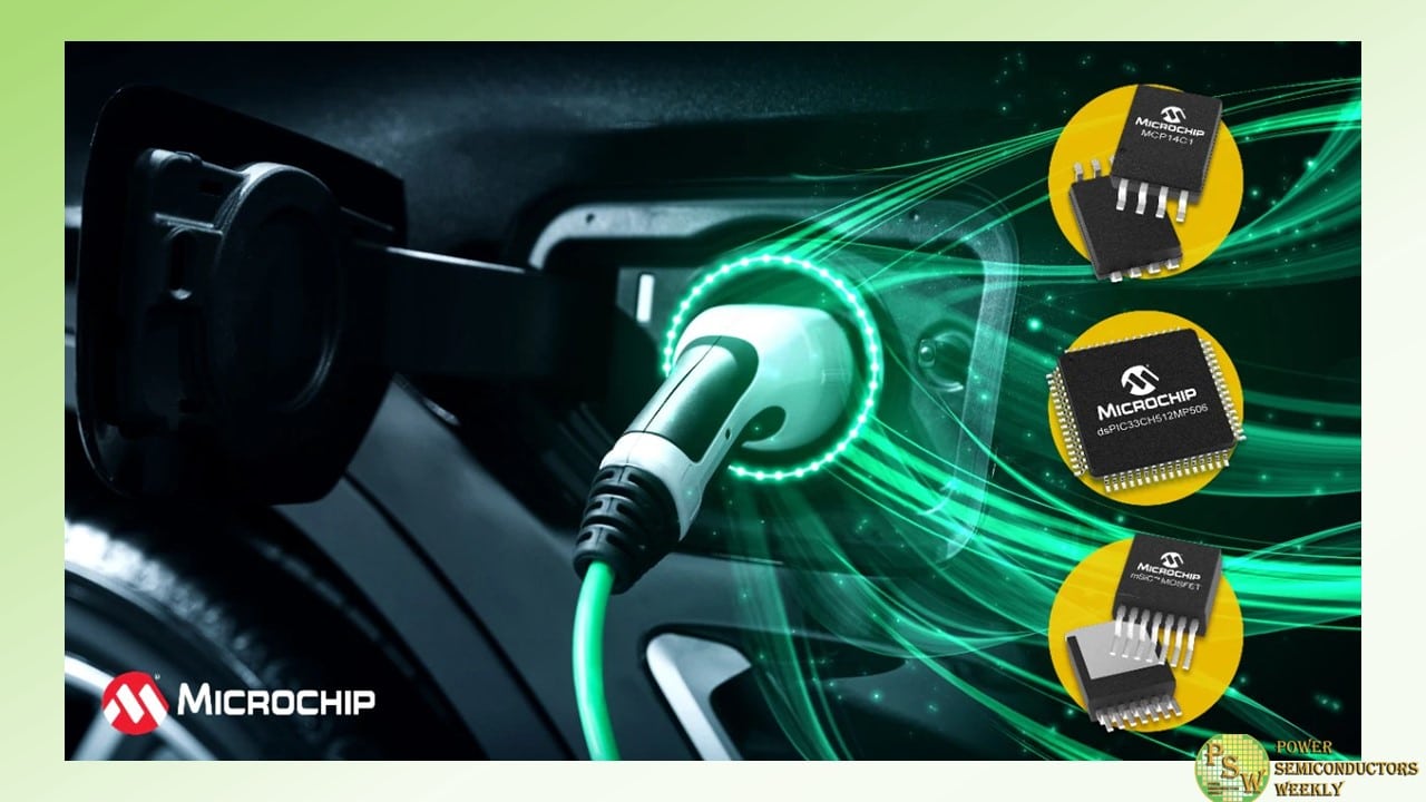
The market for Battery Electric Vehicles (BEVs) and Plug-in Hybrid Electric Vehicles (PHEVs) continues to grow as the push towards decarbonization requires sustainable solutions to reduce emissions. A critical application for EVs is the on-board charger, which converts AC power into DC power to recharge the vehicle’s high-voltage battery.
Microchip Technology announced an On-Board Charger (OBC) solution that uses a selection of its automotive-qualified digital, analog, connectivity and power devices, including the dsPIC33C Digital Signal Controller (DSC), the MCP14C1 isolated SiC gate driver and mSiC™ MOSFETs in an industry-standard D2PAK-7L XL package.
This solution is designed to increase an OBC system’s efficiency and reliability by leveraging the dsPIC33 DSC’s advanced control functions, the MCP14C1 gate driver’s high-voltage reinforced isolation with robust noise immunity and the mSiC MOSFETs’ reduced switching losses and improved thermal management capabilities. To further simplify the supply chain for customers, Microchip provides the key technologies that support the other functions of an OBC, including communication interfaces, security, sensors, memory and timing.
To accelerate system development and testing, Microchip offers a flexible programmable solution with ready-to-use software modules for Power Factor Correction (PFC), DC-DC conversion, communication and diagnostic algorithms. The software modules in the dsPIC33 DSC are designed to optimize performance, efficiency and reliability, while offering flexibility for customization and adaptation to specific OEM requirements.
“Microchip established an E-Mobility megatrend team with dedicated resources to support this growing market, so in addition to providing the control, gate drive and power stage for an OBC, we can also provide customers with connectivity, timing, sensors, memory and security solutions,” said Joe Thomsen, corporate vice president of Microchip’s digital signal controller business unit. “As a leading supplier to OEMs and Tier-1s, Microchip offers comprehensive solutions to streamline the development process, including automotive-qualified products, reference designs, software and global technical support.”
Here is an overview of the key components in this OBC solution:
- The dsPIC33C DSC is AEC-Q100 qualified and features a high-performance DSP core, high-resolution Pulse-Width Modulation (PWM) modules and high-speed Analog-to-Digital Converters (ADCs), making it optimal for power conversion applications. It is functional safety ready and supports the AUTOSAR® ecosystem.
- The MCP14C1 isolated SiC gate driver is AEC-Q100 qualified and is offered in SOIC-8 wide-body package supporting reinforced isolation and SOIC-8 narrow-body supporting basic isolation. Compatible with the dsPIC33 DSC, the MCP14C1 is optimized to drive mSiC MOSFETs via Undervoltage Lockout (UVLO) for VGS = 18V gate drive split output terminals, which simplifies implementation and eliminates the need for an external diode. Galvanic isolation is achieved by leveraging capacitive isolation technology, which results in robust noise immunity and high Common-Mode Transient Immunity (CMTI).
- The mSiC MOSFET in an AEC-Q101-qualified D2PAK-7L XL surface mount package includes five parallel source sense leads to reduce switching losses, increase current capability and decrease inductance. This device supports 400V and 800V battery voltages.
Microchip has published a white paper that provides more information about how this OBC solution can optimize a design’s performance and speed up its time to market.
For more information about Microchip’s OBC solutions for EVs, visit Microchip’s website.
Original – Microchip Technology
-
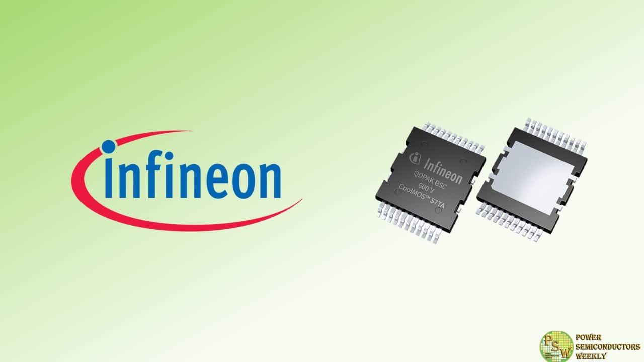
Infineon Technologies AG introduced the 600 V CoolMOS™ S7TA Superjunction MOSFET for automotive power management applications. Designed to meet the specific requirements of automotive electronics, the S7TA features an integrated temperature sensor that significantly improves the accuracy of junction temperature sensing, building on the advances made by its counterpart for industrial applications (CoolMOS S7T). The resulting benefits include improved durability, safety, and efficiency, all of which are essential in the automotive domain.
Like its industrial counterpart, the automotive-graded CoolMOS S7TA is particularly well suited for solid-state relay (SSR) applications, demonstrating superior R DS(on) and sensing accuracy, which is crucial for various automotive electronic devices that rely on efficient power management solutions. The integration of a Superjunction MOSFET with an embedded temperature sensor in the same package enhances the performance of SSRs and ensures dependable operation even under the most severe overload conditions, which is an absolute necessity for automotive applications where reliability is non-negotiable.
The embedded sensor of the S7TA offers a 40 percent increase in accuracy and up to four times faster response time than standalone on-board sensors. Such advances in temperature monitoring are critical for automotive applications, enabling individual monitoring within multi-device systems, thereby improving reliability, and preventing thermal issues that can lead to system failures.
The optimized power transistor utilization of the CoolMOS S7TA promises not only superior performance, but also precise control of the output stage. This level of precision is key to reducing power consumption and energy costs, which is a pressing concern in automotive applications where efficiency translates directly into vehicle range and operational economy. Compared to traditional electromechanical relays, the CoolMOS S7TA offers a significant improvement in total power dissipation.
The CoolMOS S7TA further provides a high overcurrent threshold, which serves to increase the reliability of the SSR and reduce the likelihood of failures. The robust switching solution paves the way for safer operations within the vehicle, and the enhanced robustness of the MOSFETs leads to a longer automotive relay lifecycle, resulting in lower maintenance and replacement costs.
The 600 V CoolMOS S7TA provides an optimized solution for potential applications that are central to the safety and functionality of modern vehicles. These include critical components such as circuit breakers, encompassing high-voltage battery disconnect switches, low-frequency switches for both direct current (DC) and alternating current (AC), as well as high-voltage electronic fuses (HV eFuses).
Infineon also introduces the EVAL_eFuse_PoC_400V_S7, a proof-of-concept board that showcases the robustness and versatility of an automotive eFuse. The board demonstrates a reliable method for safeguarding automotive electrical systems, featuring an interchangeable power stage that adapts to various operating conditions with different voltage classes and cooling methods.
Both the 600 V CoolMOS S7T in automotive and industrial grades are already available and come in QDPAK TSC and BSC packages, offering a range of R DS(on) from 17 to 40 mΩ. The 10 mΩ variant will be added to the lineup in the second half of 2024. Further information is available at www.infineon.com/s7ta and www.infineon.com/s7t.
Original – Infineon Technologies
-
Wolfspeed is expanding its portfolio of industry-leading SiC MOSFET & Schottky diode discrete products with the addition of the new Top Side Cooled (TSC) package: the U2. With options ranging from 650 V – 1200 V, Wolfspeed’s TSC products significantly increase system level power density and efficiency, while improving thermal management and board layout flexibility.
Applications:
- Electric Vehicle (EV) On-Board Chargers and Fast Charging Infrastructure
- EV & Industrial HVAC (Heating, Ventilation, and Air Conditioning) Motor Drives
- High Voltage DC/DC Converters
- Solar and Energy Storage
- Industrial Motor Drives
- Industrial Power Supplies
Features:
- Low profile, surface mount footprint
- Top side cooling with low Rth
- AEC-Q101 Automotive Qualified Options
- SiC MOSFETs Available from 750 V – 1200 V
- SiC Schottky Diodes Available from 650 V – 1200 V
Benefits:
- Highest Creepage Distance Available for SiC Top Side Cooled Packages
- Higher System Power Density with Optimized PCB Layouts
- High Volume Manufacturing Capability with Surface Mount Footprint
What’s New? Advantages of New Top Side Cooled Packages
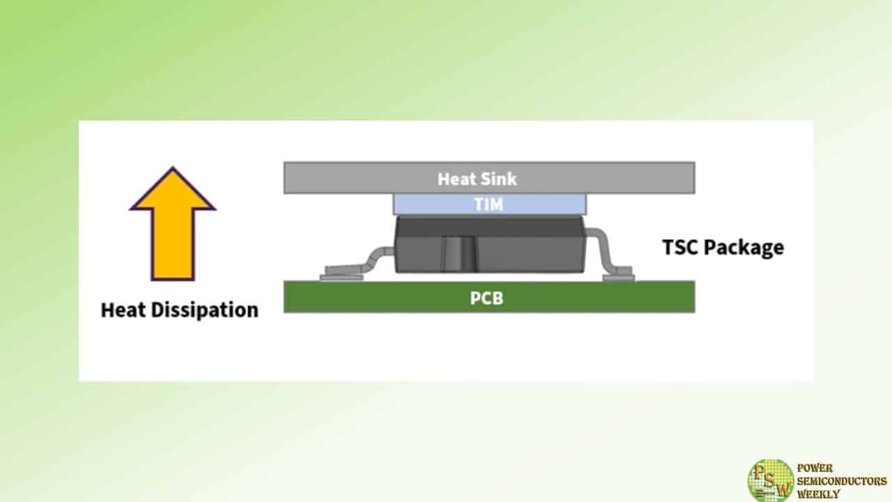
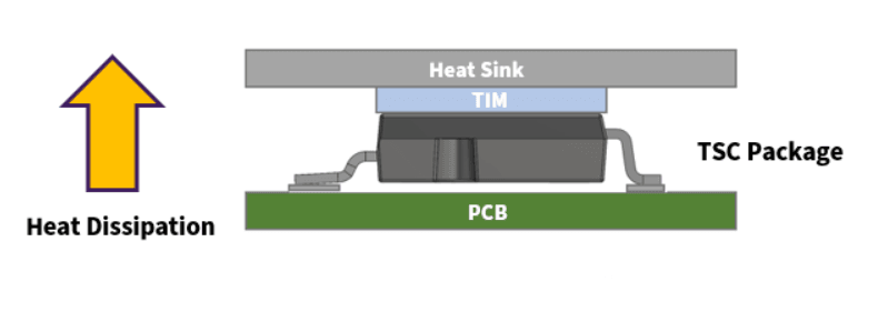
Most standard surface mount discrete power semiconductors remove heat through the bottom of the device by making direct contact with the power circuit board (PCB), which utilizes a heat sink or cooling plate attached underneath. This method is common across many different power electronics applications, particularly when size and weight requirements do not limit PCB mounting and heat sinks.
Top side cooled (TSC) devices, on the other hand, dissipate heat through the top side of the package. Inside TSC packages, the die sits upside down in the upper portion of the package to allow heat to flow directly to the top surface. Generally, TSC devices are best suited for high-performance applications such as automotive and e-mobility systems where high-power densities, advanced thermal management solutions, and small footprints are essential. Within these applications, TSC devices help address cooling requirements by enabling maximum power dissipation and optimizing thermal performance.
TSC designs also allow for dual-side usage of the PCB since the bottom board surface is no longer needed for the heatsink interface. Removing the heatsink from the thermal path not only creates an improved overall system thermal impedance; it also allows for automated assembly, which can increase manufacturing throughput for a more efficient and cost-effective solution.
Evaluating U2 TSC Devices Made Easy with SpeedVal™ Kit
Wolfspeed’s SpeedVal Kit Modular Evaluation Platform allows engineers to reduce the transition from silicon to silicon carbide (SiC) with a flexible set of building blocks for in-circuit evaluation of system performance at real operating points. The recently released 3-phase motherboard enables high-power testing with static loads as well as a foundation for advanced motor control firmware development.
Evaluation boards for a variety of Rdson ratings for Wolfspeed’s TSC MOSFET devices are coming soon.
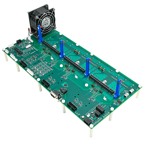
SpeedVal™ Kit Modular Evaluation Platform Three-Phase Motherboard Putting U2 TSC Devices to Work: 13 kW Automotive HVAC Motor Drive Reference Design
Wolfspeed’s upcoming 13 kW motor drive reference design, featuring the TSC U2 package, demonstrates the benefits of U2 devices for 10 kW+ EV HVAC systems, which support thermal management of the cabin, battery, and electronics. Optimizing the efficiency and operating temperature range of the HVAC system with the implementation of SiC enables systems designers to bring fast charging to the driver in under 15 minutes, while also extending the driving range per charge for the lifetime of the car. Utilizing Wolfspeed’s new CRD-13DA12N-U2 13 kW HVAC reference design, SiC enables:
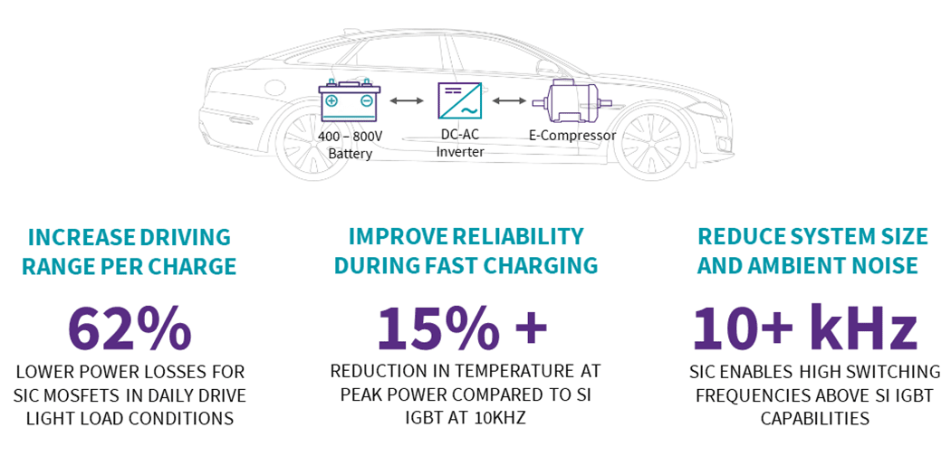
Reference Design Specifications:
- Input Voltage: 550 – 850 V
- Max Output Current: 25 A
- Max Output Power: 13 kW
- Switching Frequency: 10 – 32 kHz
- Peak Efficiency: > 98%
Original – Wolfspeed
-
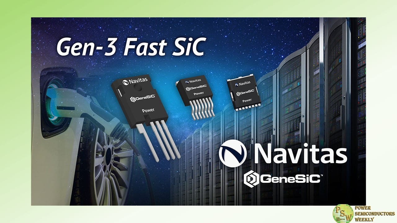
Navitas Semiconductor announced their new portfolio of Gen-3 ‘Fast’ (G3F) 650 V and 1,200 V SiC MOSFETs optimized for fastest switching speed, highest efficiency, and increased power density for applications such as AI data center power supplies, on-board chargers (OBCs), fast EV roadside super-chargers, and solar / energy-storage systems (ESS). The broad portfolio range covers industry-standard packages from D2PAK-7 to TO-247-4, designed for demanding, high-power, high-reliability applications.
The G3F family is optimized for high-speed switching performance, resulting in 40% improvement to hard-switching figures-of-merits (FOMs) compared to competition in CCM TPPFC systems. This will enable increasing the wattage of next-generation AI power supply units (PSUs) up to 10 kW, and power per rack increase from 30 kW to 100-120 kW.
The G3F GeneSiC MOSFETs are developed using a proprietary ‘trench-assisted planar’ technology. and offer better-than-trench MOSFET performance, while also providing superior robustness, manufacturability and cost than competition. G3F MOSFETs deliver high-efficiency with high-speed performance, enabling up to 25°C lower case temperature, and up to 3x longer life than SiC products from other vendors.
The ‘trench-assisted planar’ technology enables an extremely low RDS(ON) increase versus temperature, which results in the lowest power losses across the complete operating range and offers up to 20% lower RDS(ON) under real-life operation at high temperatures compared to competition.
Additionally, all GeneSiC MOSFETs have the highest-published 100%-tested avalanche capability, 30% longer short-circuit withstand time, and tight threshold voltage distributions for easy paralleling, GeneSiC MOSFETs are ideal for high-power, fast-time-to-market applications.
Navitas’ latest 4.5 kW high-power density AI Server PSU reference design in CRPS185 form-factor, showcases the 650 V-rated, 40mOhms G3F FETs for an Interleaved CCM TP PFC topology. Alongside the GaNSafe™ Power ICs in the LLC stage, a power density of 138 W/inch3 and peak efficiency above 97% is realized, which comfortably achieves ‘Titanium Plus’ efficiency standards, now mandatory in Europe.
For the EV market, 1,200 V/34 mOhm (G3F34MT12K) G3F FETs enable Navitas’ new 22 kW, 800V Bi-Directional OBC and 3KW DC-DC converter to achieve a superior power density of 3,5 kW/L and a peak efficiency of 95.5%.
“G3F sets a new standard for efficient, cool-running SiC performance, coupled with high reliability and robustness for high-power, high-stress systems,” noted Dr. Sid Sundaresan, Senior Vice President of SiC Technology and Operations. “We’re pushing the boundaries of SiC, with up to 600 kHz switching speeds, and hard-switching figures-of-merit up to 40% better than competition.”
Original – Navitas Semiconductor
-

Alpha and Omega Semiconductor Limited announced the expansion of their package portfolio options available for their second generation 650V to 1200V αSiC MOSFETs. Applicable to many critical applications such as xEV charging, solar inverters, and industrial power supplies, the new package selections give designers the added flexibility of multiple system optimization options to further maximize system efficiency while streamlining their manufacturing process.
AOS will showcase its expanded surface mount and module package options at PCIM Europe 2024 in Nuremberg, Germany, June 11-13.
The first new surface mount package is available for the AOBB040V120X2Q, AOS’ new 1200V/40mOhm αSiC MOSFET in a standard D2PAK-7L surface mount package. This AEC-Q101 qualified product is designed to replace traditional through-hole packages. It is ideal for applications such as on-board chargers (OBCs) where efficient cooling can be provided by vias and backside PCB heatsinks, simplifying the assembly flow and maximizing the power density. In addition, the low inductance package combined with the fast driver sourcesense connection positions these AOS αSiC MOSFETs as one of the most efficient power-switching solutions in the market.
For additional design flexibility, AOS is releasing its GTPAK™ surface mount package with topside cooling features. In designs where a topside-mounted heatsink is viable, the direct heat path from the GTPAK minimizes the thermal resistance. It enables higher power dissipation for more effective PCB routing. The first AOS product in GTPAK is the AOGT020V120X2. This 1200V/20mOhm αSiC MOSFET is an ideal solution to meet the requirements of high-efficiency solar inverter and industrial power supply applications.
Finally, AOS announced the AOH010V120AM2 as the first product in its new AlphaModule™ high power baseplate-less module family. This 1200V/10mOhm half-bridge αSiC module features press-fit pins and an integrated thermistor. It is in a standard footprint module that enables the replacement of multiple discrete devices into a single compact form factor while simplifying both the mechanical and electrical design by providing a clear separation of electrical and cooling paths. Single modules are suitable for residential solar inverters, or several modules in parallel will allow scaling to power levels necessary to drive the needs of fast DC charging stations.
“With the continued growth in EVs, energy infrastructure, and renewable energy, we continue to see increased interest in our αSiC MOSFETs. The expansion of our product portfolio to include these new advanced package options gives our customers the design flexibility they need to take advantage of our superior αSiC performance and continue the trend of pushing power systems to higher density and efficiency,” said David Sheridan, Vice President of SiC products at AOS.
Original – Alpha and Omega Semiconductor
-

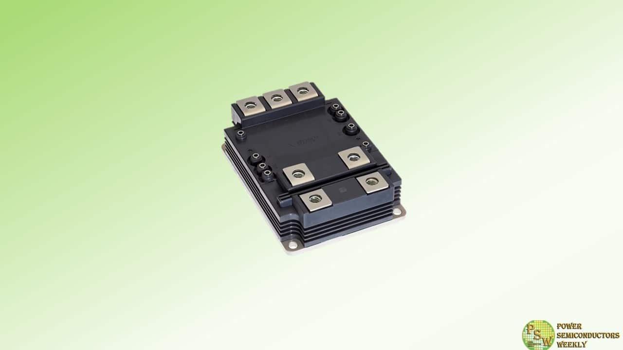
Toshiba Electronic Devices & Storage Corporation has started mass production of a 3rd generation silicon carbide (SiC) 1200 V and drain current (DC) rating 400 A of SiC MOSFET module “MG400Q2YMS3” for industrial equipment and has expanded its lineup.
The new product MG400Q2YMS3 offers low conduction loss with low drain-source on-voltage (sense) of 0.9 V (typ.). It also offers low switching loss with both turn-on switching loss and turn-off switching loss of 13 mJ (typ.). These help to reduce power loss of equipment and the size of cooling device.
MG400Q2YMS3 has a low stray inductance of 12 nH (typ.) and is capable of high-speed switching. In addition, it suppresses surge voltage in switching operation. Thus, it is available for high frequency isolated DC-DC converter.
Toshiba’s SiC MOSFET module of 2-153A1A package has a lineup of five existing products, MG250YD2YMS3 (2200 V / 250 A), MG400V2YMS3 (1700 V / 400 A), MG250V2YMS3 (1700 V / 250 A), and MG600Q2YMS3 (1200 V / 600 A), including new products. This provides a wider range of product selection.
Toshiba will continue to meet the needs for high efficiency and the downsizing of industrial equipment.
Applications
Industrial equipment
- Auxiliary power supply for railway vehicles
- Renewable energy power generation systems
- Motor control equipment for industrial equipment
- High frequency DC-DC converters, etc.
Features
- Low drain-source on-voltage (sense):
VDS(on)sense=0.9 V (typ.) (ID=400 A, VGS=+20 V, Tch=25 °C) - Low turn-on switching loss:
Eon=13 mJ (typ.) (VDD=600 V, ID=400 A, Tch=150 °C) - Low turn-off switching loss:
Eoff=13 mJ (typ.) (VDD=600 V, ID=400 A, Tch=150 °C) - Low stray inductance:
LsPN=12 nH (typ.)
Original – Toshiba
-

The electronics industry is witnessing a significant shift towards more compact and powerful systems, driven by technological advancements and a growing focus on decarbonization efforts. With the introduction of the Thin-TOLL 8×8 and TOLT packages, Infineon Technologies AG is actively accelerating and supporting these trends. They enable a maximum utilization of the PCB mainboard and daughter cards, while also taking the system’s thermal requirements and space restrictions into account.
The company is now expanding its portfolio of CoolSiC™ MOSFET discretes 650 V with two new product families housed in the Thin-TOLL 8×8 and TOLT packages. They are based on the CoolSiC Generation 2 (G2) technology, offering significantly improved figures-of-merit, reliability, and ease-of-use. Both product families specifically target high and medium switching-mode power supplies (SMPS), including AI servers, renewable energy, EV chargers, and large home appliances.
The Thin-TOLL package has a form factor of 8×8 mm and offers the best-in-class Thermal Cycling on Board (TCoB) capability on the market. The TOLT package is a top-side cooled (TSC) enclosure with a similar form factor to TOLL. Both package types offer developers several benefits: Using them in AI and server power supply units (PSU), for example, reduces the thickness and length of the daughter cards and allows for a flat heat sink.
When used in microinverters, 5G PSU, TV PSU and SMPS, the Thin-TOLL 8×8 package allows for a minimization of the PCB area occupied by the power supply devices on the mainboard, while TOLT keeps the junction temperature of the devices under control, given that these applications typically use convection cooling. In addition, TOLT devices complete Infineon’s top-side cooled CoolSiC industrial portfolio, namely CoolSiC 750 V in Q-DPAK. They enable developers to reduce the PCB footprint occupied by SiC MOSFETs when the power to be delivered to the devices does not require a Q-DPAK package.
The CoolSiC MOSFETs 650 V G2 in ThinTOLL 8×8 and TOLT are now available in R DS(on) from 20, 40, 50 and 60 mΩ. Additionally, the TOLT variant is also available with an R DS(on) of 15 mΩ. The product family will be expanded by a more granular portfolio by the end of 2024. More information is available at www.infineon.com/coolsic-gen2. Infineon will showcase the CoolSiC MOSFET 650 V Generation 2 at the PCIM in Nuremberg.
Original – Infineon Technologies
-
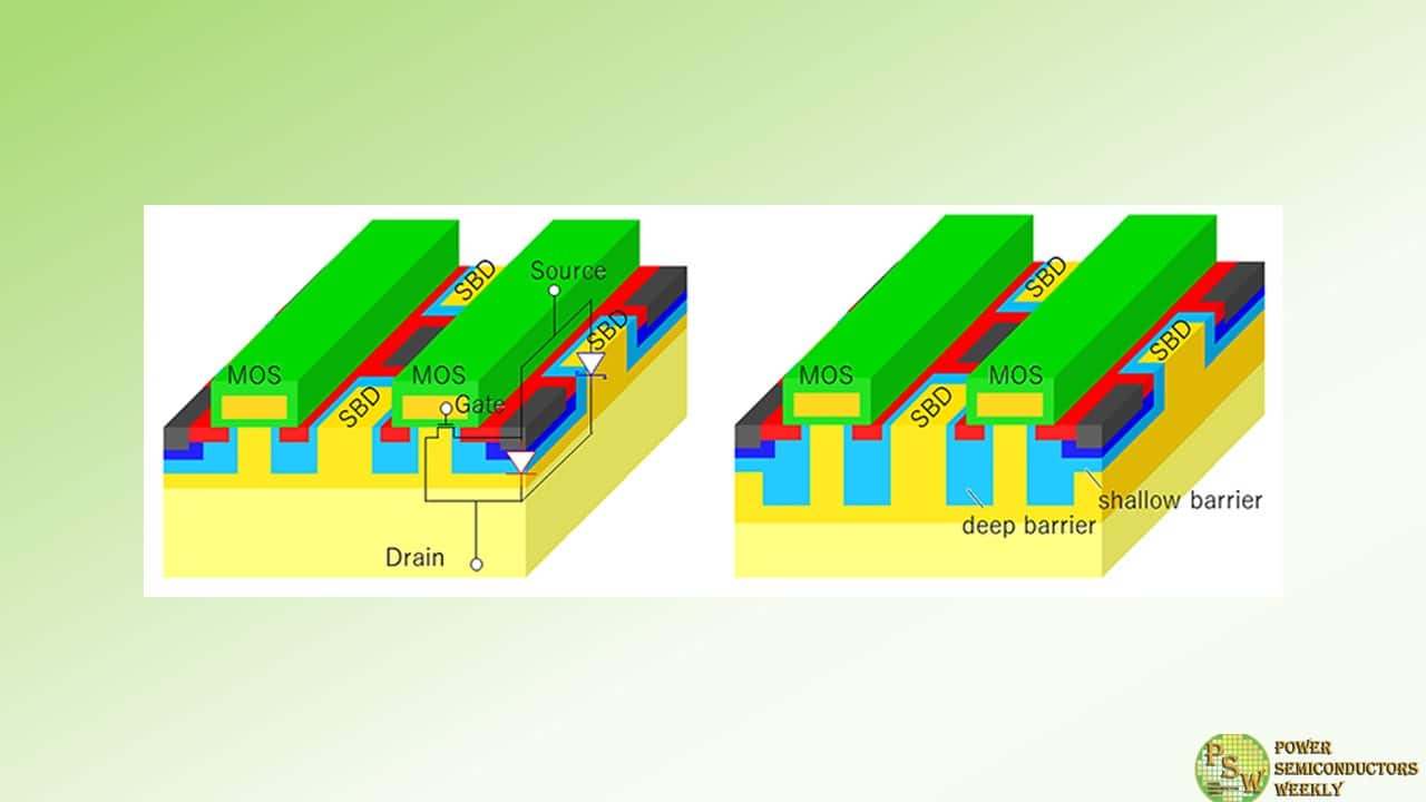
Toshiba Electronic Devices & Storage Corporation has developed a Schottky barrier diode (SBD) embedded metal oxide semiconductor field effect transistor (MOSFET), a significant improvement over the current device structure, while maintaining high reliability and short-circuit ruggedness.
A successful design modification introduces a barrier structure with varying depths in the device structure that maintains the reliability of the reverse conduction operation, the function of an integrated SBD, while suppressing the current leakage from the SBD part that causes destruction during short-circuiting. By making use of new design technology and optimizing the device structure, the new MOSFET achieves lower on-resistance (RonA), with about a 26% improvement over the current structure.
Power semiconductors play a central role in electricity supply and control. They cut energy consumption in all kinds of electronic equipment, and are an important tool for the realization of carbon neutrality. Continued demand expansion is expected from vehicle electrification and the miniaturization of industrial equipment.
Against this background, SiC MOSFETs are seen as next-generation power semiconductors. They deliver better power energy conversion efficiency than Si MOSFETs, and their use has expanded rapidly in recent years. However, SiC MOSFETs have a reliability problem: increased RonA due to reverse conduction operation. Toshiba has now developed an SBD-embedded SiC MOSFET that operates in reverse conduction without increasing RonA.
Reducing the RonA of SiC MOSFET simultaneously causes excess current flow through the MOSFET part during short-circuit operation, reducing the durability of short-circuit operation. However, enhancing the conduction of the embedded SBD to improve the reliability of reverse conduction operation increases its current leakage during short-circuit operation, which also decreases the durability of short-circuit operation.
Introducing a deep barrier structure can suppress both the excess current of the MOSFET and SBD current leakage during short-circuit operation, but it also obstructs current flow from the SBD, raising concerns about decreased reliability in diode conduction.
This led Toshiba to consider a barrier structure divided into shallow and deep areas. The deep barrier area successfully suppresses excess current from the MOSFET part during short-circuit operation, and reduces SBD current leakage, while leaving a shallow area effectively spreads current from the SBD without any obstruction by the barrier.
This improves ruggedness during short-circuit operation while maintaining excellent reliability in reverse conduction operation. Toshiba has provided some customers with test samples of SiC MOSFETs with embedded SBD that apply the new technology since December 2023 for evaluation, toward further enhancing performance.
By making use of its new design technology and optimizing the device structure, Toshiba has developed a prototype 1.2 kV class SBD-integrated MOSFET. This achieves a low RonA of 2.0 mΩcm2, about a 26% improvement over the current structure. Toshiba will present the details of this technology at The 36th International Symposium on Power Semiconductor Devices and ICs (ISPSD) 2024, an international conference on power semiconductors, which is being held in Bremen, Germany from June 2 to 6.
Original – Toshiba
