-
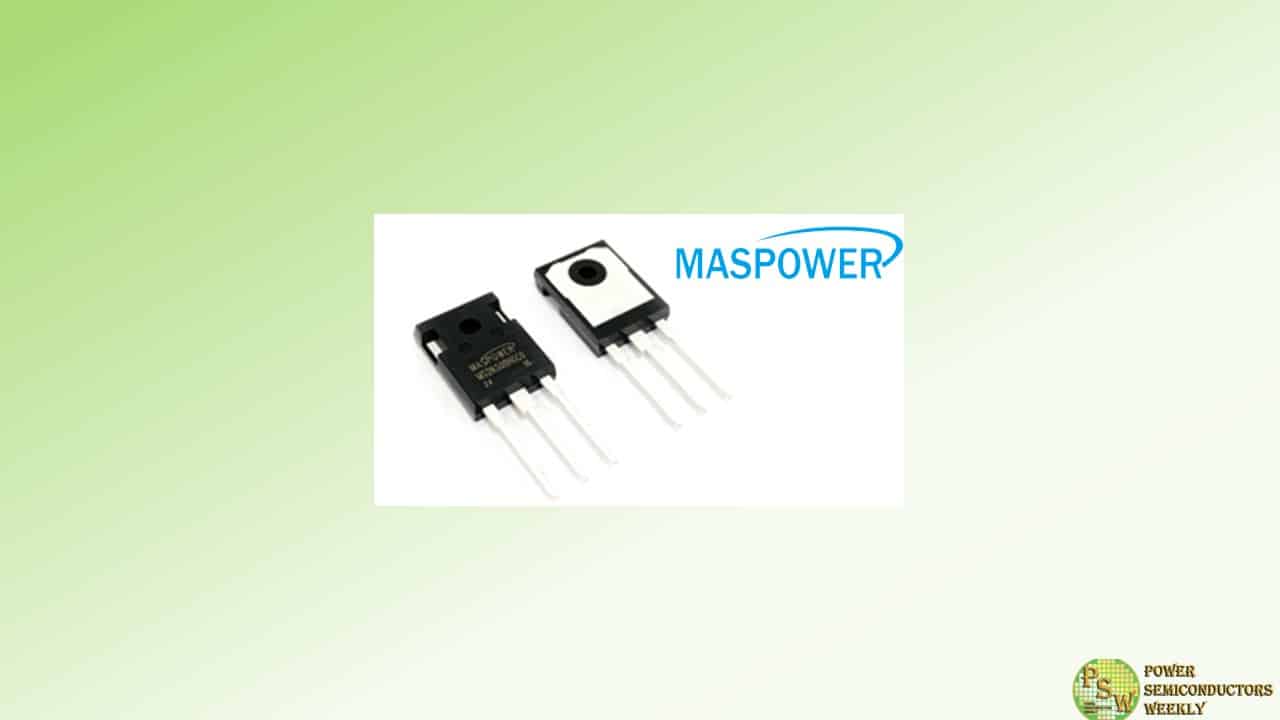
In a significant advancement for the high-voltage power electronics industry, Maspower Semiconductor has introduced the MS2N300HGC0 MOSFET, a powerful new component that sets new benchmarks in performance and reliability.
This cutting-edge product, housed in the TO-247 package, offers unprecedented performance with its robust 3000V voltage rating and 2A continuous current capability. What truly sets this MOSFET apart, however, is its rigorous testing and certification. The MS2N300HGC0 has undergone 100% avalanche testing, ensuring exceptional resilience and durability in demanding applications.
Moreover, the MS2N300HGC0’s Fast Intrinsic Diode design and minimized gate charge contribute to its high-speed switching capabilities, making it a perfect fit for high-voltage power supplies, PV inverters, switching applications and more. Its very low intrinsic capacitance further enhance its performance, delivering maximum efficiency and reliability. Maspower’s commitment to innovation and reliability is evident in the MS2N300HGC0, which has been rigorously tested and certified to meet the highest industry standards.
“The MS2N300HGC0 is a testament to our commitment to pushing the boundaries of high-voltage power electronics,” said a spokesperson from Maspower. “We are proud to offer this state-of-the-art MOSFET to our customers, enabling them to achieve unprecedented levels of performance and reliability in their applications.”
Original – Maspower Semiconductor
-
With the increasing power requirements of Artificial Intelligence (AI) processors, server power supplies (PSUs) must deliver more and more power without exceeding the defined dimensions of the server racks. This is driven by a surge in energy demand of high-level GPUs, which could consume 2 kW and more per chip by the end of the decade.
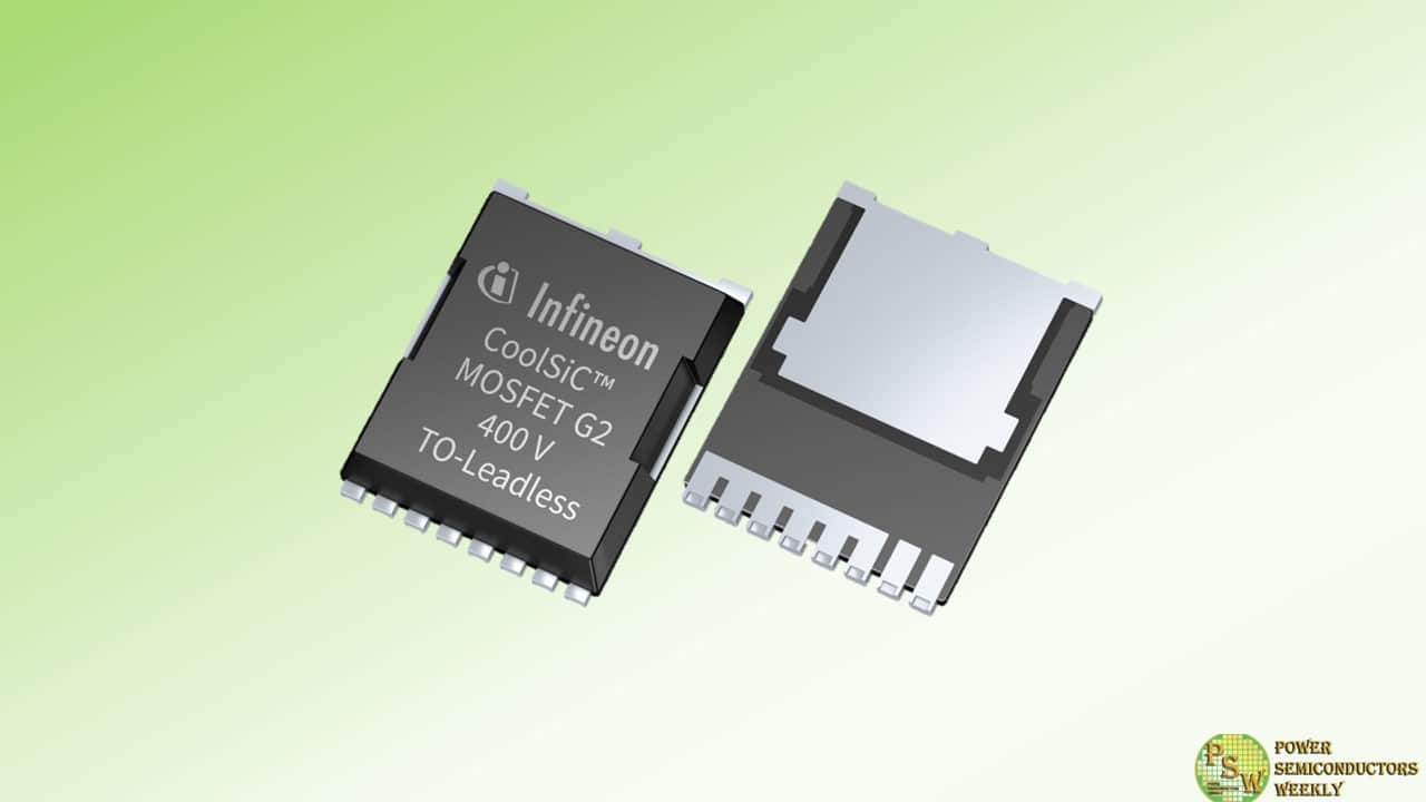
These needs, as well as the emergence of increasingly demanding applications and the associated specific customer requirements have prompted Infineon Technologies AG to extend the development of SiC MOSFETs to voltages below 650 V. The company is now launching the new CoolSiC™ MOSFET 400 V family, which is based on the second generation (G2) CoolSiC technology introduced earlier this year.
The new MOSFET portfolio was specially developed for use in the AC/DC stage of AI servers, complementing Infineon’s recently announced PSU roadmap. The devices are also ideal for solar and energy storage systems (ESS), inverter motor control, industrial and auxiliary power supplies (SMPS) as well as solid-state circuit breakers for residential buildings.
“Infineon offers an extensive portfolio of high-performance MOSFETs and GaN transistors to meet the demanding design and space requirements of AI server power supplies”, said Richard Kuncic, Head of the Power Systems Business Line at Infineon. “We are committed to supporting our customers with advanced products such as the CoolSiC MOSFETs 400 V G2 to drive highest energy efficiency in advanced AI applications.”
The new family features ultra-low conduction and switching losses when compared to existing 650 V SiC and Si MOSFETs. Implemented in a multi-level PFC, the AC/DC stage of the AI Server PSU can attain a power density of more than 100 W/in³ and is proven to reach 99.5 percent efficiency.
This is an efficiency improvement of 0.3 percentage points over solutions using 650 V SiC MOSFETs. In addition, the system solution for AI Server PSUs is completed by implementing CoolGaN™ transistors in the DC/DC stage. With this combination of high-performance MOSFETs and transistors, the power supply can deliver more than 8 kW with an increase in power density by a factor of more than 3 compared to current solutions.
The new MOSFET portfolio comprises a total of 10 products: five R DS(on) classes from 11 to 45 mΩ in Kelvin-source TOLL and D²PAK-7 packages with .XT package interconnect technology. The drain-source breakdown voltage of 400 V at T vj = 25°C. makes them ideal for use in 2- and 3-level converters and for synchronous rectification.
The components offer high robustness under harsh switching conditions and are 100 percent avalanche tested. The highly robust CoolSiC technology in combination with the .XT interconnect technology enables the devices to cope with power peaks and transients caused by sudden changes in the power requirements of the AI processor. Both the connection technology and a low and positive R DS(on) temperature coefficient enable excellent performance under operating conditions with higher junction temperatures.
Original – Infineon Technologies
-

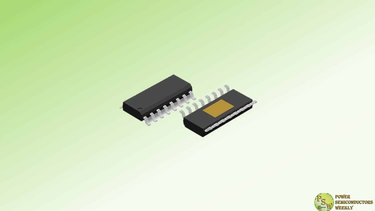
PANJIT introduced its latest 60, 100, and 150V AEC-Q101 qualified MOSFETs, engineered with advanced trench technology to set new standards in performance and efficiency. Designed for both automotive and industrial power systems, these MOSFETs offer unparalleled figure of merit (FOM), significantly lower RDS(ON), and reduced capacitance. This ensures minimal conduction and switching losses, resulting in enhanced overall electrical performance.
The new MOSFET series is available in various packages, including DFN3333-8L, DFN5060-8L, DFN5060B-8L, TO-252AA and TO-220AB-L. These compact packages facilitate efficient design solutions for modern electronic systems. With an operating junction temperature of up to 175°C, these MOSFETs are robust and reliable, further evidenced by their AEC-Q101 qualification.
These MOSFETs are ideal for various automotive applications, including wireless charging transmitters, battery management systems, front and rear lighting systems, DC/DC converters, infotainment systems and more. Their low on-resistance and high efficiency enhance the performance and reliability of these systems. Additionally, their versatility extends to industrial power systems, broadening their range of applicability and utility.
PANJIT’s new automotive-grade MOSFET series delivers superior performance, reliability, and efficiency. These MOSFETs are set to become a cornerstone in the design of next-generation automotive and industrial systems.
Original – PANJIT International
-
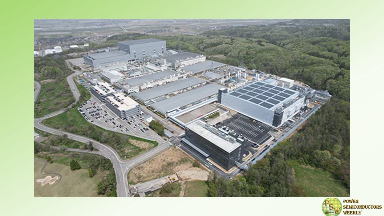
Toshiba Electronic Devices & Storage Corporation held a ceremony to mark the completion of a new 300-millimeter wafer fabrication facility for power semiconductors and an office building at Kaga Toshiba Electronics Corporation in Ishikawa Prefecture, Japan, one of Toshiba’s key group companies. The completion of construction is a major milestone for Phase 1 of Toshiba’s multi-year investment program.
Toshiba will now proceed with equipment installation, toward starting mass production in the second half of fiscal year 2024. Once Phase 1 reaches full-scale operation, Toshiba’s production capacity for power semiconductors, mainly MOSFETs and IGBTs, will be 2.5 times that of fiscal 2021, when the investment plan was made. Decisions on the construction and start of operation of Phase 2 will reflect market trends.
The new manufacturing building follows and will make a major contribution to Toshiba’s Business Continuity Plan (BCP): it has a seismic isolation structure that absorbs earthquake shock and redundant power sources. Energy from renewable source and solar panels on the roof of the building (onsite PPA model) will allow the facility to meet 100% of its power requirement with renewable energy.
Product quality and production efficiency will be boosted by the use of artificial intelligence (AI). Toshiba expects to receive a grant from the Ministry of Economy, Trade and Industry of Japan to subsidize its investment in part of the manufacturing equipment.Power semiconductors play a crucial role in electricity supply and control, and are essential devices for energy efficiency in all electrical equipment. With the continuing electrification of automobiles and the automation of industrial machinery, they are expected to see continued robust demand growth. Toshiba started power semiconductor production on a new 300-millimeter wafer line in the second half of fiscal 2022 at Kaga Toshiba Electronics’ existing facility. Going forward, the company will expand production with the new fab and further contribute to carbon neutrality.
Overview of Kaga Toshiba Electronics Corporation
Location: 1-1, Iwauchi-machi, Nomi-shi, Ishikawa Prefecture, Japan
Established: December, 1984
President and Representative Director: Satoshi Aida
Employees: 1,150 (as of March 31, 2024)
Main Products: Discrete semiconductors (power semiconductors, small-signal devices and optoelectronic devices)
Web: Kaga Toshiba Electronics CorporationOriginal – Toshiba
-
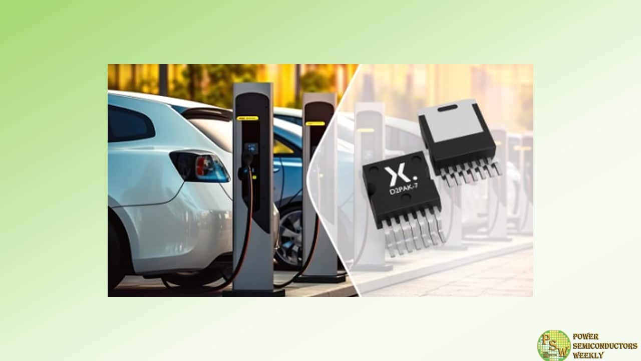
Nexperia announced that it is now offering its industry leading 1200 V silicon carbide (SiC) MOSFETs in D2PAK-7 surface mount device (SMD) packaging, with a choice of 30, 40, 60, and 80 mΩ RDSon values. This announcement follows on from Nexperia’s late-2023 release of two discrete SiC MOSFETs in 3 and 4-pin TO-247 packaging and is the latest offering in a series which will see its SiC MOSFET portfolio swiftly expand to include devices with RDSon values of 17, 30, 40, 60 and 80 mΩ in flexible package options.
With the release of the NSF0xx120D7A0, Nexperia is addressing the growing market demand for high performance SiC switches in SMD packages like D2PAK-7, which is becoming increasingly popular in various industrial applications including electric vehicle (EV) charging (charge pile, offboard charging), uninterruptible power supplies (UPS) and inverters for solar and energy storage systems (ESS).
It is also further testimony to Nexperia’s successful strategic partnership with Mitsubishi Electric Corporation (MELCO), which has seen the two companies join forces to push the energy efficiency and electrical performance of SiC wide bandgap semiconductors to the next level, while additionally future-proofing production capacity for this technology in response to ever growing market demand.
RDSon is a critical performance parameter for SiC MOSFETs because it impacts conduction power losses. However, many manufacturers concentrate on the nominal value, neglecting the fact that it can increase by more than 100% as device operating temperatures rise, resulting in considerable conduction losses.
Nexperia identified this as a limiting factor in the performance of many currently available SiC devices and leveraged the features of its innovative process technology to ensure that its new SiC MOSFETs offer industry-leading temperature stability, with the nominal value of RDSon increasing by only 38% over an operating temperature range from 25 °C to 175 °C.
Tightest threshold voltage, VGS(th) specification, allows these discrete MOSFETs to offer balanced current-carrying performance when connected in parallel. Furthermore, low body diode forward voltage (VSD) is a parameter which increases device robustness and efficiency, while also relaxing the dead-time requirement during freewheeling operation.
Original – Nexperia
-
Littelfuse, Inc. announced the launch of the IX4352NE Low-side SiC MOSFET and IGBT Gate Driver. This innovative driver is specifically designed to drive Silicon Carbide (SiC) MOSFETs and high-power Insulated Gate Bipolar Transistors (IGBTs) in industrial applications.
The key differentiator of the IX4352NE lies in its separate 9 A source and sink outputs, which enable tailored turn-on and turn-off timing while minimizing switching losses. An internal negative charge regulator also provides a user-selectable negative gate drive bias for improved dV/dt immunity and faster turn-off. With an operating voltage range (VDD – VSS) of up to 35 V, this driver offers exceptional flexibility and performance.
One of the standout features of the IX4352NE is its internal negative charge pump regulator, which eliminates the need for an external auxiliary power supply or DC/DC converter. This feature is particularly valuable for turning off SiC MOSFETs, saving valuable space typically required for external logic level translator circuitry. The logic input’s compatibility with standard TTL or CMOS logic levels further enhances space-saving capabilities.
The IX4352NE is ideally suited for driving SiC MOSFETs in various industrial applications such as:
- on-board and off-board chargers,
- Power Factor Correction (PFC),
- DC/DC converters,
- motor controllers, and
- industrial power inverters.
It’s superior performance makes it ideal for demanding power electronics applications in the electric vehicle, industrial, alternate energy, smart home, and building automation markets.
With its comprehensive features, the IX4352NE simplifies circuit design and offers a higher level of integration. Built-in protection features such as desaturation detection (DESAT) with soft shutdown sink driver, Under Voltage Lockout (UVLO), and thermal shutdown (TSD) ensure the protection of the power device and the gate driver. The integrated open-drain FAULT output signals a fault condition to the microcontroller, enhancing safety and reliability. Furthermore, the IX4352NE saves valuable PCB space and increases circuit density, contributing to overall system efficiency.
Notable improvements over the existing IX4351NE include:
- A safe DESAT-initiated soft turn-off.
- A thermal shutdown with high threshold accuracy.
- The charge pump’s ability to operate during thermal shutdown.
The new IX4352NE is pin-compatible, allowing for a seamless drop-in replacement in designs that specify the existing Littelfuse IX4351NE, which was released in 2020.
“The IX4352NE extends our broad range of low-side gate drivers with a new 9 A sink/source driver, simplifying the gate drive circuitry needed for SiC MOSFETs,” commented June Zhang, Product Manager, Integrated Circuits Division (SBU) at Littelfuse. “Its various built-in protection features and integrated charge pump provide an adjustable negative gate drive voltage for improved dV/dt immunity and faster turn-off. As a result, it can be used to drive any SiC MOSFET or power IGBT, whether it is a Littelfuse device or any other similar component available on the market.”
Original – Littelfuse
-
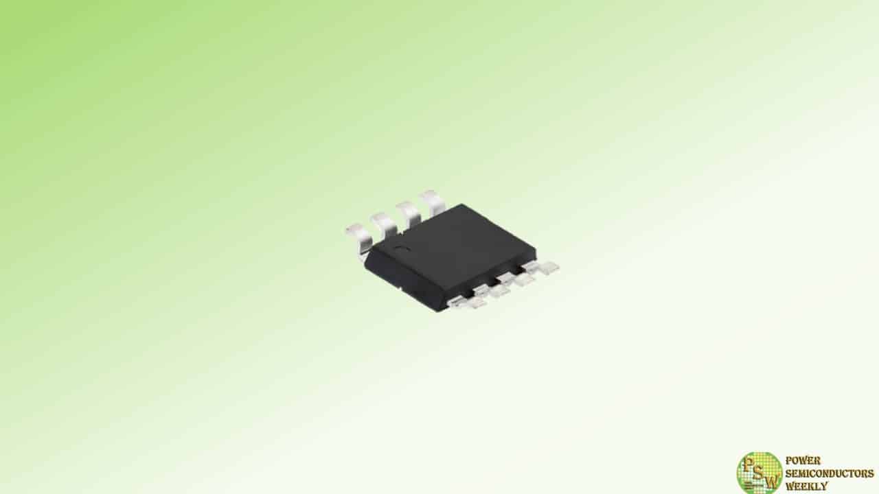
To provide higher efficiency and power density for telecom, industrial, and computing applications, Vishay Intertechnology, Inc. introduced its first fourth-generation 600 V E Series power MOSFET in the new PowerPAK® 8 x 8LR package.
Compared to previous-generation devices, the Vishay Siliconix n-channel SiHR080N60E slashes on-resistance by 27 % and resistance times gate charge, a key figure of merit (FOM) for 600 V MOSFETs used in power conversion applications, by 60 % while providing higher current in a smaller footprint than devices in the D²PAK package.
Vishay offers a broad line of MOSFET technologies that support all stages of the power conversion process, from high voltage inputs to the low voltage outputs required to power the latest high tech equipment. With the SiHR080N60E and other devices in the fourth-generation 600 V E Series family, the company is addressing the need for efficiency and power density improvements in two of the first stages of the power system architecture — power factor correction (PFC) and subsequent DC/DC converter blocks.
Typical applications will include servers, edge computing, super computers, and data storage; UPS; high intensity discharge (HID) lamps and fluorescent ballast lighting; telecom SMPS; solar inverters; welding equipment; induction heating; motor drives; and battery chargers.
Measuring 10.42 mm by 8 mm by 1.65 mm, the SiHR080N60E’s compact PowerPAK 8 x 8LR package features a 50.8 % smaller footprint than the D²PAK while offering a 66 % lower height. Due to its top-side cooling, the package delivers excellent thermal capability, with an extremely low junction to case (drain) thermal resistance of 0.25 °C/W.
This allows for 46 % higher current than the D²PAK at the same on-resistance level, enabling dramatically higher power density. In addition, the package’s gullwing leads provide excellent temperature cycle capability.
Built on Vishay’s latest energy-efficient E Series superjunction technology, the SiHR080N60E features low typical on-resistance of 0.074 Ω at 10 V and ultra low gate charge down to 42 nC. The resulting FOM is an industry-low 3.1 Ω*nC, which translates into reduced conduction and switching losses to save energy and increase efficiency in power systems > 2 kW.
For improved switching performance in hard-switched topologies such as PFC, half-bridge, and two-switch forward designs, the MOSFET released today provides low typical effective output capacitances Co(er) and Co(tr) of 79 pF and 499 pF, respectively. The package also provides a Kelvin connection for improved switching efficiency.
The device is RoHS-compliant and halogen-free, and it is designed to withstand overvoltage transients in avalanche mode with guaranteed limits through 100 % UIS testing.
Original – Vishay Intertechnology
-
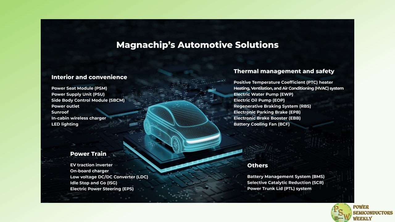
Magnachip Semiconductor Corporation announced the release of its new 40V MXT MV MOSFET. With this latest addition, the Company now offers 13 MOSFET and IGBT products for a wide range of automotive applications.
As the automotive industry adopts advanced technologies such as autonomous driving and enhanced infotainment systems, the demand for high-efficiency power solutions increases. According to Omdia, a global market research firm, the automotive power discrete market is projected to grow 14% annually from 2024 to 2027.
Magnachip entered the automotive sector in April 2022 with its first 40V MOSFET and has since broadened its product offerings by releasing 30V, -40V (P-channel MOSFET), 60V, and 250V MOSFETs for vehicles. In September 2023, the Company introduced 650V and 1200V IGBTs for positive temperature coefficient heaters and e-compressors for automotive. In the last two years, Magnachip’s power products have been integrated into vehicles of major automotive manufacturers in the United States, Korea, Japan and China.
Leveraging its technological capabilities, Magnachip now unveils this 40V MXT MV MOSFET (AMDD040N055RH) in the Decawatt Package (DPAK). The new MOSFET offers exceptional versatility for various automotive applications, such as motor control systems or power seat modules and electric stability control systems for reverse battery protection.
“Magnachip is committed to supplying premium products that meet the evolving demands of the automotive sector,” said YJ Kim, CEO of Magnachip. “Our technical innovation, coupled with a steady supply and a comprehensive range of product offerings, will strengthen our foothold in the automotive industry and broaden our global market presence.”
Original – Magnachip Semiconductor
-

Infineon Technologies AG supplies its power semiconductor devices to FOXESS, a fast-growing leader in the green energy industry and a manufacturer of inverters and energy storage systems. The two sides aim at promoting the development of green energy.
Infineon will provide FOXESS with its CoolSiC™ MOSFETs 1200 V, which will be used with EiceDRIVER™ gate drivers for industrial energy storage applications. At the same time, FOXESS’ string PV inverters will use Infineon’s IGBT7 H7 1200 V power semiconductor devices.
The global market for photovoltaic energy storage systems (PV-ES) has grown at a high speed in the last years. As competition in the PV-ES market accelerates, improving power density has become key to success, and how to improve efficiency and power density for energy storage applications has attracted much attention. Infineon’s CoolSiC MOSFET 1200 V and IGBT7 H7 1200 V series power semiconductor devices adopt the latest semiconductor technologies and design concepts that are tailored to industrial applications.
Mr. Yu Daihui, Senior Vice President and Head of Industrial & Infrastructure of Infineon Technologies Greater China said, “As an industry leader in power semiconductors, we are proud to work closely with FOXESS. We will continue to drive decarbonization by enabling higher power density and more reliable systems for PV-ES applications.”
Mr. Zhu Jingcheng, Chairman of FOXESS, said, “Thanks to the support of Infineon’s advanced components, FOXESS’ products have been significantly improved in terms of reliability and efficiency. This has been an important driving force for FOXESS’ growth. Infineon’s technical support and product quality have not only strengthened our competitiveness, but also expanded our presence in the market. We are confident about the future and look forward to further cooperation with Infineon to jointly promote the development of the industry and create greater value for our customers.”
With a high power density, Infineon’s CoolSiC MOSFETs 1200 V can reduce losses by 50 percent and provide ~2 percent additional energy without increasing the battery size, which is especially beneficial for high-performance, lightweight, and compact energy storage solutions. FOXESS’ H3PRO 15 kW-30 kW energy storage series uses Infineon’s CoolSiC MOSFETs 1200 V for all models. Thanks to Infineon’s excellent performance, the H3PRO series has achieved an efficiency of up to 98.1 percent and excellent EMC performance; with superior performance and reliability, the H3PRO series has seen rapid sales growth in the global market.
Infineon’s TRENCHSTOP IGBT7 H7 650 V / 1200 V series has lower losses and helps improve the overall efficiency and power density of inverters. In high-power inverter projects, high-current mold packaged discrete devices with current handling capability above 100 A can reduce the number of IGBTs in parallel and replace the IGBT module solution, further improving system reliability and reducing costs; in addition, the H7 series has become an industry benchmark for its high-quality performance and greater resistance to humidity.
At present, FOXESS’ main industrial and commercial model, the R Series 75-110 kW, redefines the overall design of the 100 kW model by using IGBT7 H7 series discretes, and the efficiency of the whole machine can reach up to 98.6 percent. Thanks to the low power loss and high power density of the IGBT7 H7 series in discrete packages, technical problems such as current sharing in the paralleling process can be simplified and optimized.
Every power device needs a driver, and the right driver can make the design a lot easier. Infineon offers more than 500 EiceDRIVER gate drivers with typical output currents of 0.1 A~18 A and comprehensive protection functions including fast short-circuit protection (DESAT), active Miller clamp, shoot-through protection, fault reporting, shutdown, and overcurrent protection, suitable for all power devices including CoolSiC and IGBTs.
Original – Infineon Technologies
-
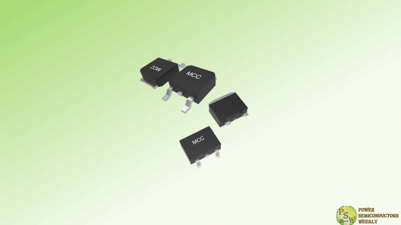
MCC Semi introduced new high-performance 40V N-channel MOSFETs. These components leverage split-gate trench (SGT) technology and full AEC-Q101 qualification in compact packages.
Both MCU2D8N04YHQ and MCB2D8N04YHQ also boast low on-resistance of only 2.8mΩ, ensuring efficient power management in a diverse range of automotive systems.
These versatile MOSFETs in high-demand DPAK and D2PAK packages ensure a seamless upgrade path with minimal changes for integration within existing designs. Adding to their unquestionable performance in harsh conditions, these components have a high operating junction temperature of up to 175°C.
Whether it’s a battery management system or electric water pump, these new MOSFETs are up for delivering the ultimate in reliability for challenging automotive applications.
Features & Benefits:
- Fully AEC-Q101 qualified
- Split-gate trench (SGT) technology
- Low RDS(on)
- High power density package
- High junction temperature up to 175℃
- Available in compact DPAK and D2PAK packages
Original – Micro Commercial Components
