-
Micro Commercial Components unveiled 1700V SiC MOSFET – SICW400N170A-BP. Designed to elevate power conversion in a range of applications, this MOSFET features ultra-low on-resistance of only 400mΩ and high blocking voltage capability. SICW400N170A-BP SiC MOSFET enables high-speed switching while ensuring minimal conduction losses — essential requirements for optimizing frequency-dependent systems.
A standard, yet durable TO-247AB package delivers effective operation at a gate-source voltage of 20V with superior thermal stability and an operating junction temperature of +175°C.
This unwavering reliability in harsh conditions only adds to the component’s appeal and versatility for various high-voltage applications, including EV charging stations and renewable energy systems.
Features & Benefits:
- High blocking voltage capability (1700V)
- Ultra-low on-resistance (400mΩ) enhances efficiency
- Low capacitance enables faster switching
- Excellent thermal stability
- High operating junction temperature (to +175°C)
- Standard TO-247AB package
Original – Micro Commercial Components
-
LATEST NEWS / Si / SiC / WBG1 Min Read
BYD honored United Nova Technology (formerly known as Semiconductor Manufacturing Electronics (ShaoXing) Corporation) with “Special Contribution Award” on BYD NEV (New Energy Vehicle) Core Supplier Convention 2023 for being a highly reliable partner in terms of quality and delivery capability.
Since 2021, UNT has engaged in broad cooperation with BYD in multi domains, including power devices such as SiC MOSFET, IGBT, and silicon-based MOSFET, as well as power modules and analog IC for automotive industry.
With the deepening of cooperation, UNT’s products have entered BYD’s ocean series and dynasty series on a large scale. In 2023, the SiC MOSFET manufactured by UNT have been widely installed in BYD’s electric vehicles. Being awarded the “Special Contribution Award” is a full recognition of the continuous contribution and outstanding performance of UNT.
In the future, UNT will continue to deepen its close cooperation with global customers such as BYD, promote technology innovations, and provide customers with more efficient and low-energy consumption solutions to support the vigorous development of the green energy.
Original – United Nova Technology
-
LATEST NEWS / PRODUCT & TECHNOLOGY / Si3 Min Read
Alpha and Omega Semiconductor Limited announced the release of two αMOS5™ 600V FRD Super Junction MOSFETs. αMOS5™ is AOS’s market and application-proven high voltage MOSFET platform, designed to meet the high efficiency and high-density needs of servers, workstations, telecom rectifiers, solar Inverters, EV charging, motor drives and industrial power applications.
The design of today’s mid-high power switched-mode power supply (SMPS) and solar inverter systems boil down to four major challenges – higher efficiency, higher density, lower system costs, and uncompromised robustness. High Voltage Super Junction MOSFETs are dominant the choice for topologies such as single/interleaved/dual boost/CrCM TP PFCs, LLC, PSFB, multi-level NPC/ANPC and so forth.
αMOS5™ has been the leading High Voltage Super Junction solution tailored for fast switching, ease-of use and robustness in mission-critical applications. αMOS5™ FRD FETs are engineered with strong intrinsic body diode to handle hard commutation scenarios, when the freewheeling body diode is in reverse recovery due to abnormal operations, such as short-circuit or start-up transients.
The two products released, the AOK095A60FD (TO-247) and AOTF125A60FDL (TO-220F), are 600V FRD FETs with 95mohm and 125mohm maximum Rdson, respectively. In tests conducted by AOS engineers, the body diodes of these two FRD FETs have survived high di/dt, under abnormal system conditions, even at elevated junction temperatures of up to 150°C. Additionally, AOS tests have shown that these devices’ turn off energy (Eoff) are noticeably lower than the competition’s, which contributes to higher efficiency in light or mid-load conditions.
“We defined our products for traditional power supplies, as well as DC/DC and DC/AC converters of solar inverters and ESS systems, where bi-directional topologies are needed. As energy storage-ready inverters become the trend and high voltage batteries are utilized increasingly in AC-coupled systems, the AOK095A60FD and AOTF125A60FDL will become industry leading solutions for bi-directional DC/DC and inverter/PFC applications that serve a wide range of power supplies, solar PV inverters, and ESS hybrid converters,” said Richard Zhang, Senior Director of Product Line and Global Power Supply Business at AOS.
Technical Highlights
- Rugged, fast recovery diode (FRD) with reduced Qrr for demanding use cases
- Engineered for both hard and soft switching topologies with ultra-low switching loss
- Strong UIS and SOA capabilities
- Engineered to prevent self turn-on
- Suitable for LLC, PSFB, CrCM Totem-Pole, Multi-level NPC and CrCM H-4/Cyclo Inverter applications
Original – Alpha and Omega Semiconductor
-
INDUSTRY PAPERS29 Min Read
Abstract
The design and optimization of power converters is a key factor in the growth and development of the power electronics field. However, the process of designing a power converter is not straightforward, and engineers often rely on experience and intuition, sometimes requiring time-consuming computer simulations. This paper presents a tool for the basic design of grid-connected AC–DC converters. The design tool takes specifications and operating conditions for two-level and three-level NPC converter topologies and derives a draft design.
The tool calculates the input filter’s electrical parameters, the converter’s losses, the temperature rise of the power semiconductor devices, and the ripple current and voltage of the DC-link capacitor. In order to validate the proposed design tool, four AC–DC converters using SiC MOSFETs were designed. Based on the design results, simulation models and prototypes were fabricated to verify the performance and confirm that the proposed design tool can be used in the basic design process of converters.
1. Introduction
As the field of power electronics continues to evolve, the design and optimization of power converters is a key factor in the efficient conversion and utilization of energy. Power converters in various forms, such as AC–DC converters and DC–DC converters, play an important role in power management, motor control, and more in a variety of applications such as renewable energy systems, electric vehicles, industrial automation, and home appliances. The ability to design these power converters precisely and efficiently is crucial for meeting the energy efficiency, reliability, and sustainability requirements of the ever-evolving energy industry [1].
However, the process of designing a power converter is far from simple. There are complex tradeoffs between design features such as the power circuit structure, control scheme, and switching frequency and performance metrics such as efficiency, voltage ripple, and current ripple. Engineers designing power converters often rely on experience and intuition, and in some cases, complex computer simulations, to achieve optimal results. Even experienced professionals can find it difficult to design with new converter topologies, control schemes, etc., and it can take a lot of trial and error to learn how to do it, especially for newcomers to the field [2,3].
To solve this problem, studies have been conducted on procedures and methods for designing various types of power converters. References [4,5,6] present step-by-step procedures for designing power converters with specific converter topologies or introduce tools that can assist in the design. These works are mainly aimed at finding the optimal design point to achieve the targeted performance metrics when the basic design of the power converter is already completed. However, this approach can be difficult for someone not already familiar with the design of this type of converter.
Recently, methods using artificial intelligence (AI) have been studied to automate and reduce the reliance on experts in the converter and controller design phase [7,8,9,10]. These methods are well suited for use in the optimization design phase for specific target systems. However, AI-based design methods have the disadvantage of requiring simulations under various specifications and operating conditions to collect data, and the selection of appropriate training methods and the training process may require a considerable amount of resources.
Alternatively, basic power converter design tools are available, often provided by power semiconductor manufacturers [11,12]. However, the applicable converter topologies are limited, and device selection is also limited by the only components manufactured by the design tool vendor.
To address these issues, this paper introduces a general converter design tool for power converter design. The research project “Development of High Efficiency Power Converter based on Multidisciplinary Design and Optimization Platform”, funded by the Korea Institute of Energy Technology and Planning (KETEP), aims to build and operate an open web-based design tool for various power conversion systems based on wide-band-gap (WBG) semiconductors [13].
The design tool proposed in this paper is intended to be used in the basic design phase and is intended to quickly check feasibility or to quickly see how a particular performance varies as a function of parameter variation. The intention is to save the user of the design tool the effort of calculating formulas or building simulation models by hand. The tool is a synthesis of state-of-the-art research and practical engineering expertise and aims to simplify and popularize the process of power converter design and optimization. It provides engineers and researchers with an intuitive and user-friendly interface, allowing them to efficiently explore different design outcomes with a large number of degrees of freedom. It enables them to optimize the design parameters and ultimately deliver a high-performance solution for their specific needs.
These design tools can help accelerate the development of power conversion systems, foster innovation, and enable the rapid adoption of new technologies. Furthermore, they have the potential to popularize power conversion design knowledge. The popularization of this knowledge can play an important role in the development of new technologies and paving the way for a more sustainable and efficient future in power electronics.
This paper introduces a general power conversion design tool for grid-connected AC–DC converters as part of the general converter design tool. The design tool developed requires the ability to allow the user to select different types of components available on the market during the design process. For this purpose, it is difficult to use data that must be obtained through complex experiments, and it is possible to use only the level of information disclosed in the datasheets provided by the manufacturers of the devices. The proposed design tool also aims to have simple formulas and design procedures so that they can be used in a lightweight web-based design tool.
The proposed design tool primarily tackles the complexity inherent in power converter design. While traditional design methods heavily rely on complex computer simulations, the proposed tool simplifies this aspect, allowing for faster, more rapid, and more accessible design iterations. By making the design process more accessible and less dependent on deep expertise, the proposed tool helps to popularize power converter design knowledge, which is crucial for promoting innovation in the field.
In the next section, the procedure for the basic system design of an AC–DC converter is presented, and the formulas used in each design step are derived. Based on the proposed design procedure, the design of converters of various specifications was carried out, and simulation models and prototypes were produced based on the designed parameters to verify the results of the design tool.
2. Design Procedures
This paper presents a design tool for grid-connected three-phase AC–DC converters using SiC MOSFETs among various types of power conversion devices. The design tool aims to facilitate the drafting of designs by engineers with little experience in converter design. Figure 1 shows the design procedure. Viewing the converter as an electrical circuit composed of lumped elements, the basic specifications, such as the input and output voltages, capacity, and converter topology, are first selected. Limits are set on the efficiency, voltage and current ripple, and temperature rise of the semiconductors, and the switching devices are selected.
The input parameters include operating conditions such as the switching frequency and power factor, along with the previously selected items. Based on the input parameters, the tool calculates the ripple of the input current, the voltage and current ripple of the DC-link, derives the electrical parameters of the input filter and the DC-link capacitor, and calculates the converter loss and temperature rise to check whether the limit conditions are met.
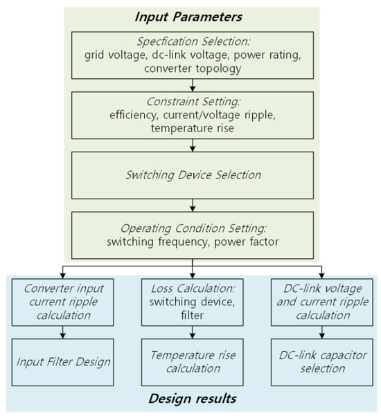
Figure 1. Grid-connected AC–DC converter design procedure.
However, this tool is intended for use in the basic design phase of a converter. In order for the web-based design tool to display design results quickly, the design procedure is based on simple formulas, and a certain amount of error is allowed. To develop a real product-level converter, more detailed design steps are required.
The component-level design of passive devices, such as inductors used in converters, component placement and mechanical structure design for power density optimization, and the electromagnetic field analysis and heat distribution analysis, which require finite element analysis, are not covered in this paper. The process and formulas used in the design tool are as follows.
2.1. Input Filter Design Procedure
In a grid-connected AC–DC converter, the purpose of the input filter is to reduce current harmonics at the input side caused by voltage harmonics generated by PWM switching. As an input filter circuit, a simple inductor or an LCL filter consisting of two inductors and one capacitor is commonly used. The design tool in this paper exploits an LCL filter that has high harmonic rejection performance per unit inductance.
Figure 2 shows the structure of the AC–DC converter and the LCL filter discussed in this paper. Lc and Lg represent the converter-side and grid-side inductors, respectively, and the filter capacitor, Cf, is connected in series with the damping resistor, Rd. The power stack is represented by a three-phase, two-level (2L) voltage-type inverter structure, which assumes the use of a three-phase, two-level or three-level (3L)-NPC converter in this paper.

Figure 2. Grid-connected AC–DC converter structure with LCL filter.
Ignoring the effect of damping resistors in the converter structure of Figure 2, the relationship between voltage harmonics and current harmonics can be expressed as follows.

where ig is the grid-side current and vc is the output voltage at the converter side. The order-specific harmonics of the output voltage due to the switching of the converter can be calculated analytically [14]. With the limits of the target harmonic currents for each order, the input filter can be designed using the relationship in (1).
Table 1, Table 2 and Table 3 show the current harmonic limits by order of the current harmonic regulations IEEE-519 [15] and IEEE-1547 [16], which are widely used in designing grid-connected AC–DC converters. Studies on designing input filters have used the relationship in (1) to select input filter parameters that ensure that the voltage harmonics caused by the PWM of the converter do not exceed the current harmonic limits of each regulation [17,18].
Table 1. Current harmonic limits according to the IEEE 519 standard [15].
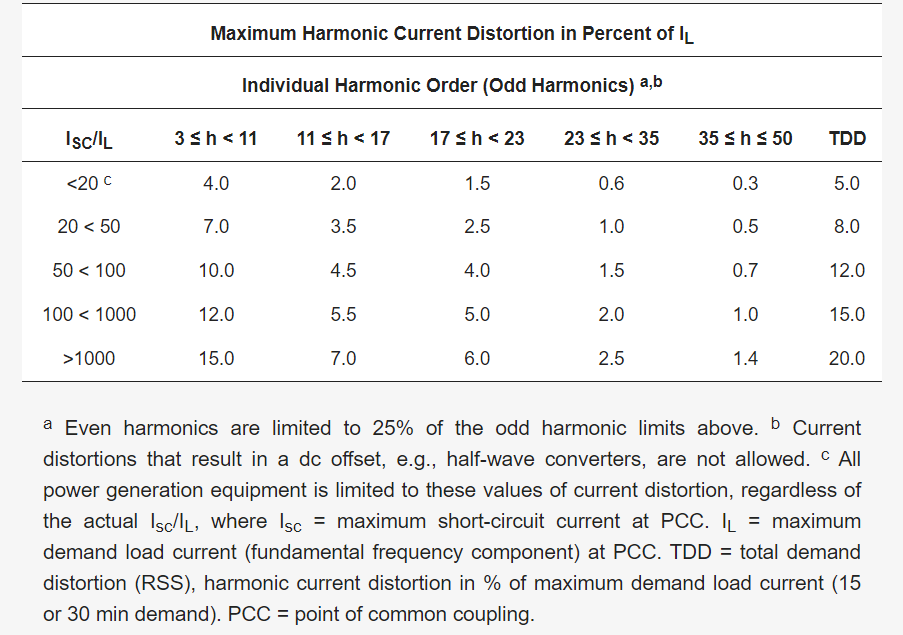
Table 2. Odd harmonic current distortion limit in percent of rated current (Irated) a according to IEEE 1547 [16].

Table 3. Even harmonic current distortion limit in percent of rated current (Irated) a according to IEEE 1547 [16].

However, this approach may not be appropriate for converters using SiC MOSFETs. As shown by the relationship in (1), harmonics in the grid current are caused by harmonics in the output voltage due to the PWM operation of the converter. The output voltage harmonics can be roughly divided into two classes according to their order: higher-order harmonics around multiples of the PWM switching frequency and lower-order harmonics corresponding to multiples of the fundamental wave, such as the 5th, 7th, 11th, etc.
The higher-order voltage harmonics can be calculated analytically according to the PWM method by obtaining the magnitude of the harmonic voltage of each order, and filter parameters can be designed accordingly to limit the harmonic current of that order to a target value or less.
However, higher-order harmonics often account for a smaller proportion of the total current harmonic component generated by a grid-tied converter than lower-order harmonics. This is because higher-order harmonics have higher frequencies and are more easily attenuated by the input filters.
This is especially true for converters using SiC MOSFETs, which often have switching frequencies of tens of kHz or more. Furthermore, popular grid input current harmonic regulations, IEEE 519 [15] and IEEE 1547 [16], limit the harmonic frequency to no more than the 50th order of the fundamental wave. For converters using SiC MOSFETs, most have switching frequencies above 20 kHz, so the higher-order harmonics associated with the switching frequency are well beyond the 50th order when referenced to the typical grid frequency of 60 Hz, which is outside the harmonic regulation criteria.
When using input filters to satisfy grid current harmonics regulations, it is then necessary to design them with low-order current harmonics in mind, but it is difficult to accurately calculate the magnitude of the voltage harmonics that cause low-order current harmonics.
Low-order output voltage harmonics are due to the non-ideal output characteristics of the converter, such as dead time and a voltage drop across switching elements, and are difficult to obtain analytically. In addition, for converters using SiC MOSFETs with fast switching frequencies, harmonic current controllers can be used to significantly suppress low-order harmonics [17]. In practice, harmonic current controllers are often used, which can lead to overly large filter designs if their effects are not considered. However, the harmonic control performance of the controller is also difficult to accurately estimate at the filter design stage.
In this paper, an input filter design method based on limiting the maximum value of the ripple of the converter-side current below a certain value is used, rather than limiting the grid current harmonics below a certain value according to the regulations of [15,16], etc. The design procedure of the input filter is shown in Figure 3, and the detailed design process is as follows.
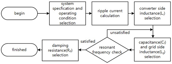
Figure 3. Inpul filter design procedure.
- Select system specifications and operating conditions. Select the grid voltage, grid frequency, converter type (2L or 3L-NPC), switching frequency, DC-link voltage, and rated current.
- Calculate ripple current and select converter side inductance. Set the converter-side ripple current limit. Select the limit value of the peak-to-peak amplitude of the current ripple relative to the rated current and calculate the converter-side inductor value that satisfies the ripple current according to the operating conditions. The peak-to-peak amplitude of the ripple current generated by the converter is determined by the operating conditions, and the instantaneous phase angle and can be expressed as (2) [18].

where Vdc is the DC-link voltage, Ts is the switching period, and r(m,θ) is a function of the voltage modulation index (m) and the output voltage phase angle (θ). The magnitude of the instantaneous current ripple depends on the phase angle, but the proposed method calculates the magnitude of the current ripple based on the output voltage at a phase angle of 90°.
In general, the power factor of a grid-connected converter is close to unity, so the output voltage and current are almost in-phase, and the magnitude of the current flowing in the converter is maximized around 90 degrees. Therefore, when considering the maximum current flowing through the converter due to current ripple, it is appropriate to base the design on the value when the phase angle is 90°. The converter-side inductance (Lc) value that satisfies the magnitude of the ripple current can be selected by using (2).
- Select capacitance and grid-side inductance. The larger the capacitor of the LCL filter, the better it can absorb the converter’s ripple current and reduce the harmonics of the grid-side current. However, the capacitor in the input filter introduces reactive power at the grid side and changes the grid side power factor. Typically, the reactive power flowing into the capacitor is limited to 2–5% of the apparent power in the design of the input filter [19]. The proposed design tool takes the reactive power value of the capacitor as input and selects the capacitor divisor of the corresponding filter. The formula for selecting the capacitance value is shown in (3).

where S is the apparent power of the converter, ω is the frequency of the grid, Vph is the phase voltage of the grid, and R is the ratio of the reactive power to the apparent power. In studies dealing with LCL filter design, the values of the grid-side inductance and the converter-side inductance are often chosen to be equal. This is because, when the resonant frequency of the LCL filter is first determined, equalizing the two inductance values results in the smallest magnitude of the total inductance [20], i.e., the harmonics of the grid current can be reduced the most with the same inductance value.
However, in this paper, the filter is designed based on the ripple current on the converter side, not the current harmonics delivered to the grid. In the case of converters using SiC MOSFETs, the low-order harmonics that contribute most to the grid current harmonics can be significantly suppressed by current controllers, so the proposed method focuses more on the converter-side inductor in the total inductance used in the input filter. In this paper, the grid-side inductance is selected as one-third of the converter-side inductance.
- Check the resonant frequency of the input filter. The resonant frequency (fres) of the input filter should be less than one-half of the sampling frequency (fs) according to the Nyquist sampling theory, and it should be higher than the bandwidth (fb) of the current controller to avoid affecting the current control behavior [21].

Finally, check whether the parameters of the input filter selected satisfies (4), and if not, adjust the capacitance value so that the resonant frequency satisfy the limitation of (4).
- Select damping resistor. The LCL filter theoretically has zero impedance at its resonant frequency. The damping resistor is used to provide impedance at this time to suppress the oscillation of the current at the resonant frequency. For this purpose, the value of the damping resistor is designed to be similar to the impedance of the capacitor connected in series at the resonant frequency [22], and in this paper, it is selected as one-third of the impedance of the capacitor at the resonant frequency.

2.2. Calculating Losses and Temperature Rise
The losses of the converter covered in this paper are composed of the losses of the power semiconductor and the losses of the input filter. The losses are calculated based on the given converter specifications and operating conditions, and the junction temperature is estimated using the thermal resistance information of the heat sink where the power semiconductor is installed.
The losses of the power semiconductor can be divided into conduction losses and switching losses. The conduction losses of SiC MOSFETs and diodes are calculated using the Rds, Rd, and Vf0 information in the datasheet, as shown in (6) and (7), respectively, and the switching losses of SiC MOSFETs are calculated using the datasheet loss data, as expressed in (8).

where Rds is the equivalent resistance when the SiC MOSFET is turned on and Rd and Vfo are the equivalent resistance and threshold voltage when the diode is turned on, respectively. Irms is the rms value of the current flowing in each power semiconductor device, fsw is the switching frequency, s(θ) is duration when the current is flowing in that semiconductor device, Iavg is the average current in the current flowing section, Vdc is the DC-link voltage, Vtest is the test voltage indicated in the switching loss data in the datasheet, and Eon/off is the loss function extracted from the on and off switching loss data in the datasheet. The gate resistance is inputted by the user and reflected in the determination of Rds and Eon/off.
Equation (8) uses the average current in the conducting section to calculate the switching losses under the assumption that the current flowing in the device at the time of switching is proportional to the switching losses. In practice, the two are not exactly proportional. In general, for SiC MOSFETs, there is a slight exponential increase in switching losses as the current flowing through the device at the time of switching increases.
As a result, the switching losses calculated from the average current tend to be smaller than the actual switching losses at higher load currents, leading to calculation errors. However, since the design tool presented in this paper is intended to be used in the basic design phase for feasibility checks, this level of error can be justified. Overcurrent and overvoltage due to parasitic components like stray inductance also affect the switching loss [23]. However, the parasitic component cannot be anticipated during the basic design phase, so it is not reflected.
Figure 4 shows the leg structure of the two-level and three-level converters covered in this design tool, and the output voltage command and output current of the converter are shown in (9) and (10).

where V and I represent the magnitude of the output voltage command and output current, respectively, ω is the frequency of the grid, and φ is the load angle. In order to calculate the loss of each power semiconductor device, the operating region can be divided into four according to sign of output voltage command and output current.
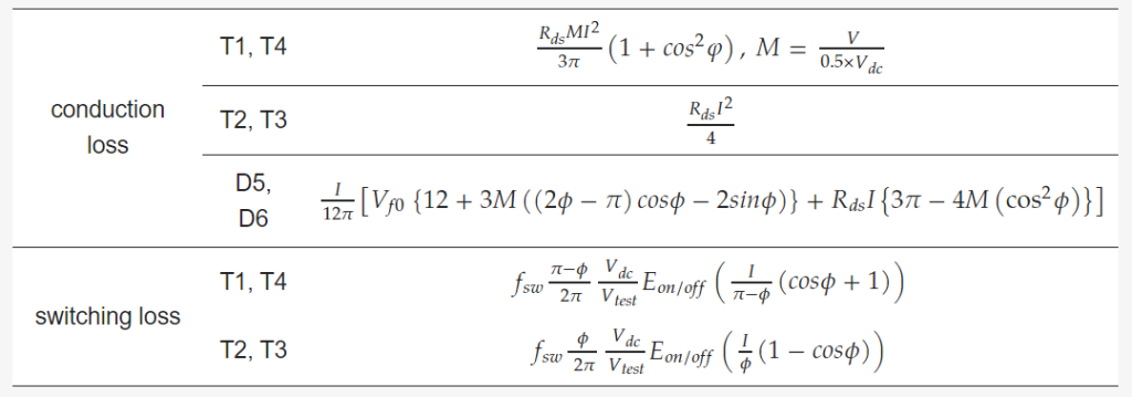
Figure 5 shows the four operating areas with the state of the output voltage command and current. Table 4 summarizes the current-carrying devices and devices where switching losses occur in each operating area for 2L and 3L-NPC converters. Using Figure 5 and Table 4, it is possible to calculate the rms value of the current flowing through each power semiconductor element, the average current in the section where the current flows, and substitute the values into (6)–(8) to calculate the loss for each element in each converter, as shown in Table 5 and Table 6.
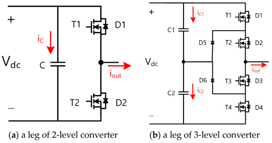
Figure 4. Leg configuration of AC–DC converters.
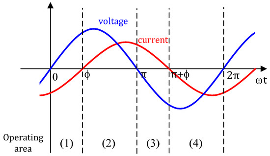
Figure 5. Operating area classification.
Table 4. Switch operation according to operating area.
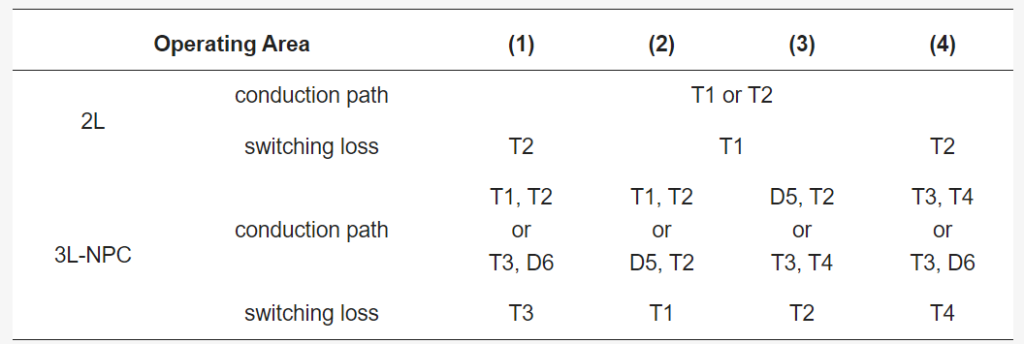
Table 5. Power semiconductor loss for 2L converter.

Table 6. Power semiconductor loss for 3L-NPC converter.
The calculated losses of the power semiconductor are used to calculate the junction temperature rise of the power semiconductor. Figure 6 shows the heat transfer circuit model used to calculate the temperature rise in this paper. The losses generated by the power semiconductor are denoted as Ploss, and the thermal resistance from the junction of the power semiconductor to the case, the thermal resistance from the case to the heat sink, and the thermal resistance from the heat sink to the atmosphere are denoted as Rth,jc, Rth,ch, and Rth,ha, respectively. Tjunction, Tcase, Theatsink, and Tamb represent the junction, case, heatsink, and ambient temperatures, respectively.
The heat capacity of each part is not considered, but only steady-state losses and thermal resistance are considered to calculate the junction temperature. Rth,jc and Rth,ch use the datasheet values of the semiconductor device, and Rth,ha of the heat sink can be entered to be used to calculate the temperature rise, as shown in (11).


Figure 6. Heat transfer circuit.
More precisely, thermal resistance could be expressed as a function of temperature [24]. However, as shown in [24], for accurate modeling, the parameters should be obtained through testing for each component used in the converter, which is difficult to achieve with a basic design tool for various different types of components. The thermal resistance in this paper uses nominal values from the datasheet.
Most of the losses in the input filter come from the inductor. The loss of the inductor is determined by the design conditions, such as the core and winding used in the inductor, and the operating conditions, such as the magnitude and frequency of the voltage and current applied to the inductor. The conduction losses of an inductor are calculated using the resistance calculated from the cross-sectional area and length of the inductor windings, and the effective value of the current flowing in the inductor and the iron losses are calculated using the Steinmetz equation shown in (12) [25].

The coefficients required for the Steinmetz equation were obtained from the core’s datasheet information and added together by calculating the losses at the fundamental and switching frequencies. The flux density (B) was calculated using the magnitude of the fundamental wave current and the maximum ripple current magnitude, calculated using (2).
2.3. DC-Link Voltage, Current Ripple Calculations
The design tool in this paper derives the minimum DC-link capacitance values required during the converter design process. With the given system specifications and operating conditions, the DC-link capacitor currents of the 2L and 3L-NPC converters (iC of the 2L converter and iC1/iC2 of the 3L-NPC converter in Figure 4) can be calculated analytically, as shown in (13) and (14), respectively [26,27]. Table 7 shows the detailed formulas for the parameters used in (14).

Table 7. Expressions of A, B, C, and D in (14).

Taking the limit value of the voltage ripple as the input, the minimum value of the DC-link capacitor that satisfies the limit value can be selected as follows [26].

The tool selects the minimum value of the DC-link capacitor through equation (15) and derives the minimum value of the ripple current rating of the capacitor through (13) or (14).
3. Design Examples
Many cases of grid-connected AC–DC converters were designed using the converter design tool introduced in this paper. Table 8 shows the specifications and operating conditions of the design cases. All of them are 10 kVA-class grid-connected AC–DC converters and use 2L and 3L-NPC NPC converter topologies.
The grid to which they are connected is assumed to be typical three-phase 380 V 60 Hz converters. The current ripple ratio indicates the magnitude of the ripple current relative to the rated current. Cases 1 and 2 and cases 3 and 4 have identical specifications except for the current ripple specification, resulting in designs with different input filters.
Table 8. Specification and operating conditions for design cases.

Table 9 shows the minimum values of the input filter and DC-link capacitance derived from the design tool. In (2), the current ripple magnitude of the 2L converter is generally larger compared to the 3L-NPC converter, resulting in a larger inductance despite the higher current ripple limit of the 2L converter.
The minimum value of the DC-link capacitor resulting from the design is less than 10 μF, so in practice, the converter design should be based on selecting a capacitor that meets the current ripple rating. In such a design, the capacitance of the actual capacitor used is considerably larger than the minimum capacitance derived from the design tool, so that the voltage ripple caused by the current ripple is negligible.
Table 9. Input filter design results.

4. Simulation and Experimental Results
Based on the results of the design tool introduced in this paper, simulation models and prototypes were produced and compared with the design values. For the four cases of circuits in Table 8 and Table 9, simulation models were created using PSIM (version 9.0), and prototypes were fabricated and compared with the experimental results.
Figure 7 is a photo of the experimental set of one of the fabricated prototypes. The current ripple of the fabricated converter was measured using an oscilloscope, and the efficiency was measured using a power meter. The temperature rise was measured by attaching an NTC to the heatsink where the power semiconductor was installed.
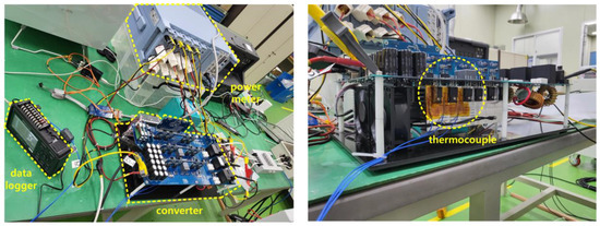
Figure 7. Experimental setup with prototype converter.
Figure 8 shows the waveforms of the fabricated simulation and the prototype. They represent the input line voltage, converter current, and grid current, respectively. It can be seen that the experimental waveforms have similar characteristics to the simulation results and behave appropriately.
Both the experimental and simulation results show that the ripple of the converter-side current varies with the circuit topology and the parameters of the input filters, but the harmonics of the grid-side current are not significantly different in all four cases. It can be seen that the low-order harmonics, which have a significant impact on the grid-side current quality, are sufficiently suppressed by the current controller.
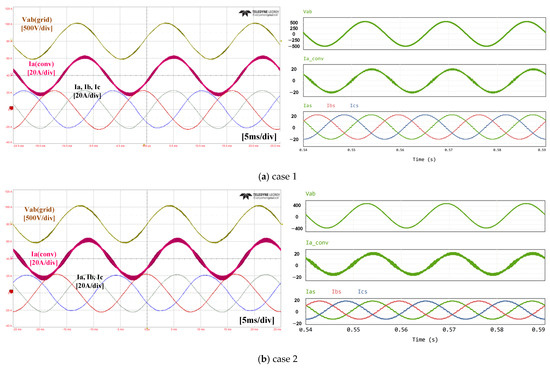
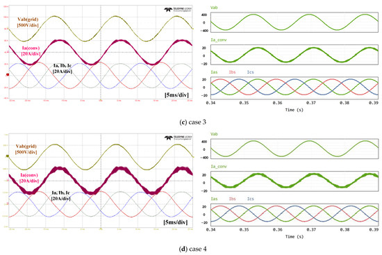
Figure 8. Experimental and simulation waveforms.
Table 10 shows the design values and experimental results of the current ripple, temperature rise, and THD of the grid current. For these metrics, only results at a rated load are compared, as their maximum values are considered during the design phase. The current ripple is similar to the design value for the 2L converter, while the 3L-NPC converter shows more deviation from the design value. In the 3L-NPC converter, the parasitic inductance along the switching path is larger due to the increase in the number of power semiconductor devices and the complexity of the busbar structure of the PCB, and the voltage spikes generated during switching have the effect of making the current ripple larger.
The THD of the grid-side current is not considered in the design tool introduced in this paper, but the measured current THD is shown to confirm that the input filter, considering only the converter-side ripple current, can keep the current THD low enough if a sufficiently good PR controller is used under a fast switching frequency. The temperature rise was calculated by measuring the temperature of the heatsink near where the power semiconductor is attached, as shown in Figure 7. In the model in Figure 6, the power semiconductor losses were calculated as Ploss and compared to Theatsink’s calculations and measurements.
The heatsink model was calculated with a simple concentrated integer thermal resistance, and the temperature of three heatsinks near the power semiconductor was measured and averaged. For the 2L converter, the temperature rise difference between the design and experimental results is smaller, but for the 3L-NPC converter, the deviation is relatively larger. In the case of the 2L converter, the number of semiconductor devices and the size of the heat sink are smaller, so the heat transfer structure is simpler and more in line with the simple model in Figure 6, but in the case of the 3L-NPC converter, the placement structure of the power semiconductor devices and the heatsink is relatively more complex, which is estimated to cause a slight deviation from the model.
Table 10. Current ripple, THD, and temperature rise of design value and experimental results.

Figure 9 shows the calculated efficiency of the design tool and the measured efficiency from the experiment. The losses in the power semiconductor and the losses in the input filter were used to calculate the efficiency. Overall, the deviation between the measured and calculated efficiency at low loads is large, and the error decreases as the load factor increases.
At light loads, the iron losses in the input filter account for a large portion of the total losses, and it is assumed that the iron losses calculated through (12) are different from the actual losses incurred, leading to the error. The flux density is used as an input variable to calculate the iron loss in Equation (12). In the proposed design tool, the flux density is derived based on the maximum value of the current ripple calculated in (2).
However, in practice, the magnitude of the current ripple varies with the phase angle [28]. In the phase section where the current ripple is reduced, the flux density is also reduced, resulting in smaller iron losses. As a result, the calculated value of iron loss is larger than the actual value. Further improvements in flux density variation according to phase angle may be needed to increase the precision of the iron loss calculation. However, as a tool used in the basic design phase of a converter, it can be considered to have a reasonable calculation error. It is also appropriate that the calculation error is reduced under heavy loads, as efficiency at higher load factors is generally considered more important.
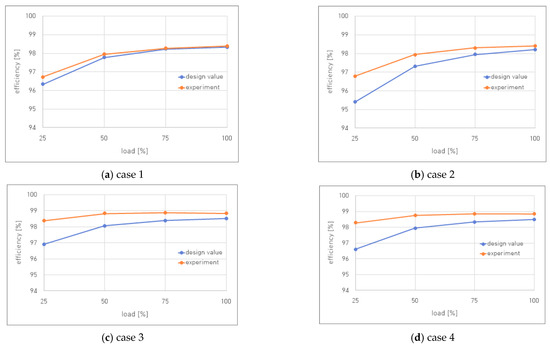
Figure 9. Efficiencies vs. loads of design value and experimental results.
5. Conclusions
This paper presents a design tool for designing three-phase grid-connected AC–DC converters. The basic design procedures for drafting the system design of a 2L or 3L-NPC converter were introduced, and the theory and formulas used in each design procedure were presented. The introduced design tools view the converter as an electrical circuit composed of lumped elements and set basic specifications, such as the input and output voltages, capacitance, converter topology, and limit conditions, such as the efficiency, voltage and current ripple, and temperature rise, and select switching elements.
Based on the input parameters, the ripple of the input current, DC-link voltage, and current ripple are calculated to derive the electrical parameters of the input filter and DC-link capacitor, and the converter losses and temperature rise are calculated to verify that the limit conditions are met.
The input filter uses the LCL filter structure, which is widely used in grid-connected converters. To limit the converter-side ripple current, the converter-side inductor value is determined first, and the grid-side inductor value is set accordingly. The capacitor value is determined according to the user-entered reactive power magnitude limit, and the damping resistor value is set to make the impedance of the input filter at the resonant frequency large enough.
Then, to calculate the efficiency, the converter losses are calculated. There are two main types of losses discussed in this paper: power semiconductor losses and input filter losses. The power semiconductor losses are calculated using the device’s datasheet information. The rms and average current flowing in each device are calculated and applied to the datasheet information of the power semiconductor device to calculate the conduction and switching losses.
The temperature rise is calculated using the thermal resistance information of the semiconductor device, the heatsink, and the previously calculated losses of the semiconductor device. The losses of the input filter are calculated by calculating the copper and iron losses of the inductor.
The current ripple in the DC stage is calculated analytically using the given system specifications and operating conditions. The calculated current ripple is used to find the minimum value of the DC-link capacitor that satisfies the voltage ripple given as a limit.
Using the introduced design tool, the converter design for various conditions is carried out and validated through a simulation and experiment. For four 10kVA-class converters, the design tool was used to derive the parameters of the input filter and the minimum value of the DC-link capacitor, and simulation models and prototypes were built based on the derived values and compared with the results of the design tool.
The experimental results showed that the temperature rise and current ripple magnitude were similar to the results of the design tool. The measured efficiency showed some deviation from the calculated value in the light-load region, but overall, the trend of efficiency change with load factor was similar in the design value and the experimental result, and the difference in the absolute values was small, showing that it is suitable as a basic design tool.
Authors
Original – MDPI
-
INDUSTRY PAPERS25 Min Read
Abstract
This paper investigates and compares the static performance and short-circuit (SC) robustness of 1200 V SiC MOSFETs with varying JFET widths (WJFET = 2.0–5.0 μm). Short-circuit measurements as well as electrical-thermal simulations are used to identify thermal distribution and maximum electrical field, providing valuable insights into the design limits. The devices under test (DUTs) with narrow and wide WJFET exhibit different failure mechanisms under SC stress.
After the short-circuit failure, interlayer dielectric (ILD) cracks are observed in DUTs with narrow JFET width (WJFET < 3 μm). In contrast, it is discovered that the burn mark is located in the channel region of the device with a wide JFET width. Moreover, the short-circuit withstand time (SCWT) of DUTs with narrow and wide WJFET exhibits varying trends under high temperature conditions (100 °C). These results can help verify the different failure mechanisms and determine an optimal JFET design to improve the trade-off between the static performance and SC ruggedness of the SiC MOSFETs.
1. Introduction
SiC MOSFETs have already emerged as one of the most crucial components in power electronic systems. They can be utilized at frequencies exceeding 100 kHz, which can facilitate a reduction in the volume of passive components and enhance the power density of the system [1]. MOSFETs are gaining increasing popularity in electric vehicles (EVs), hybrid electric vehicles (HEVs), and railways, with a growing interest in their reliability and robustness.
Approximately 38% of inverter failures can be attributed to the failure of power devices induced by short-circuit (SC) stresses [2,3,4]. During the device operation, unexpected circuit faults may occur. For example, in the half-bridge circuit, failures often arise from short circuits in the upper or lower bridge devices, and the device channel may accidentally conduct current when the device withstands the high drain voltage. This high current density flowing through the device can lead to device failure.
Numerous investigations have been conducted on the short-circuit characteristics of commercial SiC MOSFETs. The results of the short-circuit test provide valuable information about the SiC MOSFET’s ability to handle short-circuit faults without suffering permanent damage. It helps in determining the device’s short-circuit withstand capability, evaluating the effectiveness of its protection mechanisms, and assessing its thermal management strategies [5].
This knowledge is crucial for designing reliable power electronic systems that utilize SiC MOSFETs and ensuring their safe operation under various fault conditions. The short-circuit performance of SiC MOSFET power modules under various operating conditions has also been studied [6,7]. Compared to Si IGBTs, the short-circuit withstand time (SCWT) of SiC MOSFETs is 80% shorter due to their larger current densities and higher electrical fields [7]. During the short-circuit (SC) process, the heat generated in SiC MOSFETs leads to a rapid increase in the junction temperature, exceeding 1000 °C [8,9].
The rapid increase in junction temperature induces thermal and mechanical stress on the interface between aluminum and the interlayer dielectric. This stress has been observed to cause cracks at the corner of the interlayer dielectric, as reported in references [10,11]. The oxide thickness, Pwell doping and channel length have been extensively studied in SiC MOSFETs [12,13,14]. Channel structure on the short-circuit capability of SiC MOSFETs has been investigated. The impacts of channel design parameters, such as doping profiles and dimensions, are compared, offering guidelines for optimizing the channel structure for enhanced short-circuit performance [15].
The impacts of gate structure on the short-circuit performance of SiC MOSFETs are explored. Different gate designs influence the device’s ability to handle short-circuit events, providing insights into optimizing the gate structure for improved short-circuit withstand time [16]. However, the short-circuit robustness of SiC MOSFET with different JFET widths and the optimal design for JFET width are still under investigation. JFET width is the vital parameter in SiC MOSFET, which not only affects the on-resistance, electrical field at oxide, but also influences the saturate current and short-circuit characteristics.
The device researcher always focuses on the optimal parameters in static performance, but the comparison of short-circuit characteristics of switches with different JFET widths needs to be evaluated. Furthermore, devices from various manufacturers have different value (Commercial device of A company has the width of 1.75 μm. Commercial device of B company has the width of 2.8 μm).
In this study, SiC MOSFETs with various structural parameters are fabricated and their impacts on short-circuit capability are investigated. The correlation between short-circuit withstanding time and measurement temperature is studied. Electrical-thermal simulations are used to identify thermal distribution and maximum electrical field, providing valuable insights into the design limits. Additionally, device failure mechanisms are analyzed based on experimental and simulation results for different structure designs. Finally, the optimal structure design of SiC MOSFETs is summarized for improving the trade-off relationship between device conduction performance and short-circuit ruggedness.
2. Materials and Methods
2.1. Static Characteristics of SiC MOSFETs with Different Structural Parameters
As shown in Figure 1, the JFET width (WJFET) is one of the key structural parameters for SiC MOSFETs, which significantly affects both device performance and reliability. To study its impact on short-circuit ruggedness, 1200 V SiC MOSFETs with various WJFET (2.0, 2.5, 3.0, 4.0, and 5.0 μm) are fabricated in this work. In the fabricated SiC MOSFETs, the channel doping is 1 × 1017 cm−3, the drift region doping is 8 × 1015 cm−3 and the drift thickness is 12 μm. The fabrication flow is shown in Figure 2. In SiC MOSFET, the JFET region is located between two adjacent P well regions.
And P well—Nepi—P well is like JFET (junction field effect transistor), so this region is named the JFET region. Due to the intrinsic depletion region, the real current path is narrower than the dimension of WJFET. To optimize, the minimal resistance and minimize electrical field are at the center of gate oxide (<3 MV/cm).
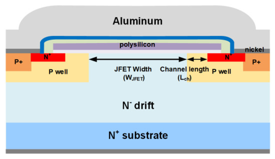
Figure 1. The schematic diagram of the 1200 V SiC MOSFET.
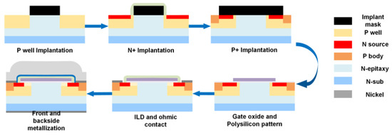
Figure 2. Manufacture flow of the 1200 V SiC MOSFET.
The five SiC MOSFET devices in this study are labeled A1–A5. The devices have identical active areas and chip sizes. In this section, the static characteristics of the five MOSFET devices are measured and analyzed.
The transfer, output and blocking I–V (current-voltage) characteristics of the five devices are measured by Keysight B1505A equipment and the results are compared in Figure 3. For the transfer I–V characteristics, the drain-source voltage (VDS) is set to 10 V in the measurement. For the output I–V characteristics, the gate-source voltage (VGS) is set to 20 V. For the blocking I–V characteristics, the VGS is set to 0 V. Device performance indexes, such as threshold voltage, resistance, transconductance and breakdown voltage are extracted and summarized in Table 1.
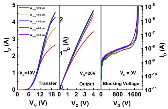
Figure 3. Static characteristics of SiC MOSFETs with different JFET widths.
Table 1. Static characteristics of SiC MOSFETs with different JFET widths.
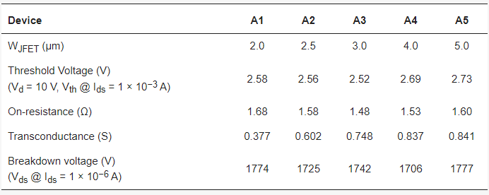
With increasing WJFET design, the threshold voltage initially decreases from 2.58 to 2.52 V, and then increases to 2.73 V. Correspondingly, the on-resistance decreases from 1.68 to 1.48 Ω, and then increases to 1.6 Ω. The transconductance of the device gradually increases from 0.377 to 0.841 S. Besides, from the blocking characteristics, all five devices can successfully achieve blocking voltages above 1700 V.
The on-resistance of a SiC MOSFET device is composed of channel resistance, JFET region resistance, drift layer resistance and substrate resistance. For 1200 V SiC MOSFETs, JFET region resistance contributes around 30% of the total resistance at room temperature. Increasing the WJFET can help reduce the JFET region resistance. However, it can also result in an increase in the cell pitch and a decrease in channel density, if the source region width remains constant. According to the experimental results, Device A3 with WJFET = 3 μm achieves the lowest resistance of 1.48 Ω among the five designs.
The output characteristics of the five devices are measured at 25 to 175 °C to investigate the conduction performance of SiC MOSFETs at high temperatures. The on-resistances at different temperatures are presented in Figure 4. It can be observed that the on-resistance increases with temperature for all five devices, but the temperature coefficient of resistance varies for different WJFET designs.
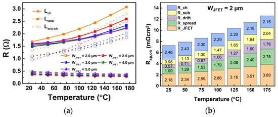
Figure 4. (a) Compositional channel resistance and total resistance at elevated temperature. (b) Compositional resistance in Device A1.
The channel resistance of VDMOS is determined by calculating the resistance of lateral long channel MOSFET and converting it based on channel length and width, as seen in Figure 4. The channel resistance accounts for more than 30% of the total resistance. The channel resistance decreases as the temperature increases from room temperature to 175 °C. At higher temperatures, the threshold voltage of the device decreases, resulting in an increased generation of electrons in the channel. Furthermore, higher electron densities in the channel provide a better screening effect, reducing the Coulomb scattering caused by interface traps.
These two factors contribute to the overall reduction in channel resistance [12]. Apart from the channel resistance, the bulk resistance exhibits a positive temperature coefficient, which is due to the lower mobility of carries at elevated temperatures caused by acoustic scattering. The opposite temperature behaviors of the channel resistance and bulk resistance components lead to the different trends in total resistance at elevated temperatures for devices with different WJFET. With a narrower JFET width, the JFET resistance becomes a larger proportion of the total resistance. Consequently, the total resistance increases more rapidly at elevated temperatures.
For Device A1, with a narrow WJFET design (2.0 μm), the JFET region resistance contributes significantly to the total on-resistance. It also has a positive temperature coefficient, resulting in the highest slope among the five devices in Figure 3. For Device A5, with a wide WJFET design (5.0 μm), the JFET region resistance contributes only a small portion to the total on-resistance. In contrast, the channel resistance plays a more significant role in determining the overall resistance of Device A5.
The negative temperature coefficient of the channel resistance in Device A5 counterbalances the positive temperature coefficient of JFET region resistance, drift layer resistance and substrate resistance. Thus, the slope of the curve for Device A5 in Figure 3 is the lowest among the five devices. For Device A3 to A5, the on-resistances are less sensitive to ambient temperature, which is good for high temperature applications. The slight increase in on-resistance with temperature is beneficial for balancing current in parallel connections.
The devices’resistance types are channel resistance, JFET resistance, drift resistance and substrate resistance, as shown in Figure 4, and the resistance is mainly based. To illustrate the reason for the transconductance and on-resistance exhibiting different trends, the different compositional resistance needs to be separated, as shown in Figure 4b. Transconductance is mainly controlled by channel resistance, as the channel resistance is dependent on the gate voltage. If the channel resistance occupies a larger portion in the on-resistance, the transconductance is higher. In five types of DUTs, the wider WJFET has a larger portion of channel resistance, so the transconductance is higher.
WJFET influence the cell pitch and also have a large impact on JFET resistance. When WJFET decreases, smaller cell pith results in the reduced channel resistance. However, narrower WJFET leads to increased JFET resistance, which is a trade-off in different devices. Among five types of devices, the WJFET = 3 μm is the optimal value.
2.2. Short-Circuit Capability of SiC MOSFETs
A short-circuit (SC) test platform has been established. Figure 5a illustrates the test bench, while Figure 5b presents the schematic diagram of the test board. The device under test (DUT) is connected in series with an IGBT device and a current shunt. A pulsed gate-source voltage is applied to the gate terminal of the DUT, and the duration of the short circuit is controlled by the pulse width. The duration of the short-circuit time gradually increased until the device reaches a failure state. In this section, we compare the short-circuit withstand time (SCWT) of SiC MOSFETs with different WJFET designs. We also analyze the device failure mechanisms, considering various device designs and different bus voltages.
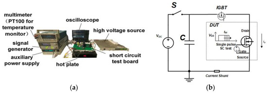
Figure 5. (a) Short-circuit test bench. (b) Schematic diagram of the SC test board.
3. Results
3.1. Short-Circuit Capability of SiC MOSFETs with Different JFET Widths at 400 V
The on and off gate-source voltages (VGS) are 20 and −5 V, respectively. The bus voltage is 400 V, and the short-circuit duration time is increased with a step of 0.5 μs until the device fails. The last non-destruction short-circuit current waveforms for different device designs are illustrated in Figure 6a. According to the figure, the SCWT of Device A1, A2, A3, A4, and A5 are 19.0, 18.5, 17.0, 15.0 and 14.0 μs, respectively. Device A3 with WJFET = 3.0 μm demonstrates the highest peak current due to the lowest on-resistance, as discussed in Section 2.
On the other hand, the SCWT gradually decreases with the increase in WJFET. The changes in peak current and SCWT with WJFET are summarized in Figure 6b. The typical waveform of gate voltage and drain current for the destruction test are shown in Figure 6c. After the destruction test, it is observed that the gate is shorted to the source terminal for all five devices. When the WJFET is increased from 2.0 to 3.0 μm, devices with wider WJFET exhibit higher peak currents.
The higher peak currents result in increased energy dissipation, which can lead to a rapid rise in junction temperature and a reduction in SCWT. However, when JFET width is further increased from 3.0 to 5.0 μm, both the peak current and SCWT decrease. It is evident that wide WJFET design devices are likely to experience different failure mechanisms compared to devices with narrower WJFET designs.

Figure 6. (a) The SC current waveforms of five types of devices with different JFET widths at Vds = 400 V. (b) Extracted SC peak current and SCWT in devices with varied JFET widths. (c) Failure waveform including gate and drain waveforms.
The failure mode is checked with blocking characteristic measurements after device failure, which are shown in Figure 7. After device failure, Device A2 with WJFET = 2.5 μm remains almost the same blocking voltage (Figure 7a) as a fresh device, while Device A5 with WJFET = 5.0 μm shows degraded blocking capability (Figure 7b). OBIRCH (Optical Beam Induced Resistance Change) is utilized to find out the failure spot.
The failure spot in Device A2 is located in the active region, as shown in Figure 8a. FIB (Focus Ion Beam) analysis is employed to observe the cross-section at the failure spot. Figure 8b displays the obtained cross-sectional result of Device A2. Cracks are observed in the ILD (interlayer dielectric) between gate polysilicon and source metal in Device A2. However, for Device A5, different observations are shown. The failure spot is also observed in the active region, as shown in Figure 8c. When the device is stripped in solvents to expose the SiC layer’s surface, a burn mark is found between the JFET region and the channel region. The top view of the device is illustrated in Figure 8d.
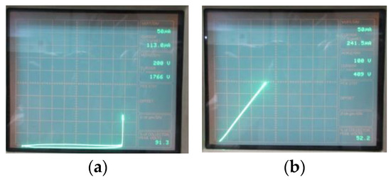
Figure 7. Blocking characteristic after short-circuit failure. (a) Device A2 with WJFET = 2.5 μm. (b) Device A5 with WJFET = 5.0 μm.

Figure 8. (a) The hot spot is observed under OBIRCH (Optical Beam Induced Resistance Change) of Device A2 at drain voltage of 400 V. (b) The cross-section at hot spot is prepared by FIB (Focus Ion Beam) of Device A2 at drain voltage of 400 V. (c) The hot spot is observed on Device A5 at drain voltage of 400 V. (d) Top view of the failure spot of Device A5 at drain voltage of 400 V after the ILD and top metal is dissolved.
To explain the failure mechanism, the TCAD is used to simulate the short-circuit procedure in SiC MOSFETs. The SiC/SiO2 interface mobility model is established, taking into account the presence of interface traps. The integration of the interface trap is coulomb charge named Nc. Varying the interface trap density at the SiC/SiO2 interface leads to differences in the short-circuit current waveform, as demonstrated in Figure 9a.
With the lower interface trap density, the peak current is higher, and more heat is generated in the SiC MOSFET. The interface trap distribution is determined by extracting the interface trap from the MOS capacitance. Figure 9b shows the comparison between the simulation results (using Dit = 3 × 1011 cm−2eV−1) and the corresponding measurement results. The simulation model is established and the temperature can be extracted through the simulation.
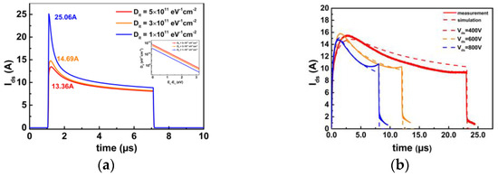
Figure 9. (a) Different interface trap density is established by applying coulomb scattering considering interface trap model. (b) Comparison between measurement and simulation result by using proper model.
For Device A2, the cracks found at ILD are due to the unmatched coefficient of thermal expansion (CTE) between different materials [17]. With higher temperatures, the CTE becomes larger [18,19]. The temperature distribution during the SC procedure at the ILD corner is calculated using a simulation tool, and the result is shown in Figure 10. Consequently, the dominant failure mechanism is the junction temperature rise caused by the energy dissipation within the device during the short-circuit pulse.
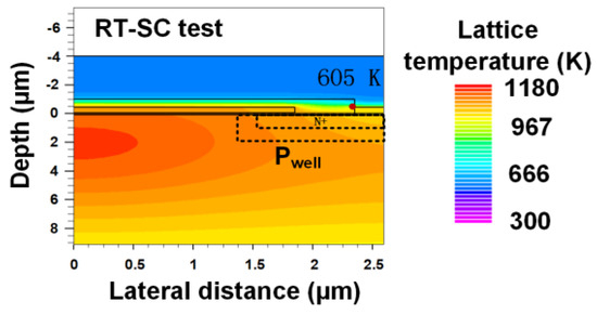
Figure 10. Simulated ILD and source metal temperature during the SC procedure.
For Device A5, the failure mode could be different. To investigate the failure mode, the short-circuit transient process is simulated using TCAD. Due to the wide WJFET design, the electrical field at SiC surface (upper in JFET region) is higher than that in Device A2, resulting in a higher impact ionization. The impact ionization within Device A5 is shown in Figure 11a. Higher impact ionization leads to an increase in hole and electron current densities. A comparison of the hole and electron current densities can be seen in Figure 11b. As the electric field direction points from SiC to the gate in the JFET region, the holes would inject into the gate oxide due to the combined effect of electric field and high kinetic energy resulting from the elevated temperature.
Additionally, in the channel region, the channel electron density in Device A5 is also higher than that in Device A2. Both the holes in the JFET region and electrons in the channel region have the potential to degrade the gate oxide and lead to device failure. To identify the main reason, a repetitive short-circuit test is conducted. The voltage shift direction indicates whether there is hole injection (negative shift) or electron injection (negative shift).
Device A2 and Device A5 are measured during a repetitive short-circuit test with Vds = 400 V, a pulse width of 6µs and Vgs,on/Vgs,off = 19 V/−5 V. When the cycle time is low, the device with a wider JFET width is influenced more by hole injection than electron injection, as observed in the comparison of the two devices in Figure 12a. However, Device A2 is primarily affected by electron injection. With repetitive cycle increasing, the electron injection becomes dominant due to the hot electron effect, as shown in Figure 12b.
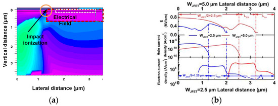
Figure 11. (a) Impact ionization in Device A5 WJFET = 5.0 μm. (b) Comparison of electrical field and hole current density at surface between Device A2 (WJFET = 2.5 μm) and Device A5 (WJFET = 5.0 μm).
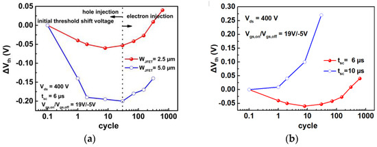
Figure 12. (a) Threshold voltage shift of device with different WJFET after repetitive short-circuit test. (b) Threshold voltage shift for different short-circuit pulse widths (6 and 10 μs).
3.2. Short-Circuit Capability of SiC MOSFETs Measured at Elevated Temperature
Short-circuit tests are carried out at an ambient temperature of 100 °C to verify the failure mechanisms for Device A2 and Device A5. The SC current waveforms are shown in Figure 13a. The peak current and SCWT for the five WJFET designs are extracted from the figure and summarized in Figure 13b. The correlations between SC peak current (SCWT) and WJFET observed at 100 °C are similar to the results obtained at 25 °C (refer to Figure 6b).
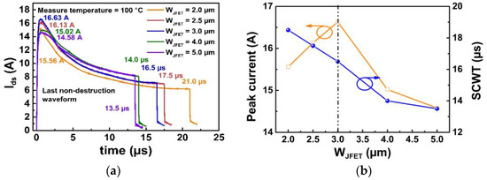
Figure 13. (a) The SC current waveforms of five types of devices with different JFET widths at Vds = 400 V at elevated temperature (100 °C). (b) Extracted SC peak current and SCWT in devices with varied JFET widths at elevated temperature (100 °C).
To study the impacts of ambient temperature on SCWT test results for different WJFET designs, the results obtained at 25 °C and 100 °C test conditions are compared in Figure 14a. The results indicate that wide WJFET designs (WJFET ≥ 3 μm) exhibit an increase in SCWT at elevated temperatures—namely, SCWT demonstrates a positive temperature coefficient for wide WJFET designs.
The increase in SCWT can be attributed to reduced electron injection into the gate oxide at elevated temperatures. Figure 14b compares the short-circuit current waveforms for the 25 and 100 °C test conditions, with tsc = 3 μs used as an example. The peak current at 100 °C is lower than that of 25 °C due to the limitations of acoustic scattering at elevated temperatures, resulting in reduced election injection for the 100 °C test condition.
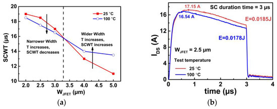
Figure 14. (a) Relationship between SCWT and JFET width under 25 and 100 °C. (b) Comparison of SC current at 25 and 100 °C under the SC duration time of 3 µs.
On the other hand, for narrow WJFET designs (WJFET < 3.25 μm), SCWT decreases at elevated temperatures. The junction temperature is calculated using simulation software. Figure 15 shows the temperature distribution within the device during the short-circuit transient at both 25 °C (Figure 15a) and 100 °C (Figure 15b). Elevated ambient temperatures result in higher junction temperatures. The thermal and mechanical stress can cause cracks in ILD layers, and higher temperatures result in a larger coefficient of thermal expansion mismatch [11].
Thus, the SCWT is decreased at elevated temperatures. In order to figure out whether failure mechanism is changed in the device with wider WJFET, failure spot of Device A4 after SC test under 100 °C is detected shown in Figure 15c. Compared with the results shown in Figure 8b, the ILD crack becomes the main failure reason for the device with wide WJFET.

Figure 15. Simulated ILD and source metal temperature during the SC procedure under (a) room temperature and (b) the elevated temperature. (c) The cross-section at hot spot is prepared by FIB (Focus Ion Beam) of Device A5 at drain voltage of 400 V after SC test under 100 °C.
3.3. Short-Circuit Capability of SiC MOSFETs with Different JFET Widths at Varied Vds Measured at Room Temperature
The SC capability of SiC MOSFETs is measured under different bus voltages (400, 600 and 800 V). The short-circuit pulse width (tSC) is gradually increased from 3 μs in steps until DUT fails. The increment step is set to 0.5 μs for 400 V, 0.3 μs for 600 V and 0.1 μs for 800 V, respectively. The short-circuit current waveforms for the five devices tested under a high bus voltage of 800 V are illustrated in Figure 16. The peak current varies among different WJFET designs. For Device A1–A3 with narrow WJFET designs, the peak current is higher than the other two designs, resulting in a shorter SCWT. Additionally, in Device A2, an interlayer crack is observed after the SC test under 800 V in Figure 17a,b.
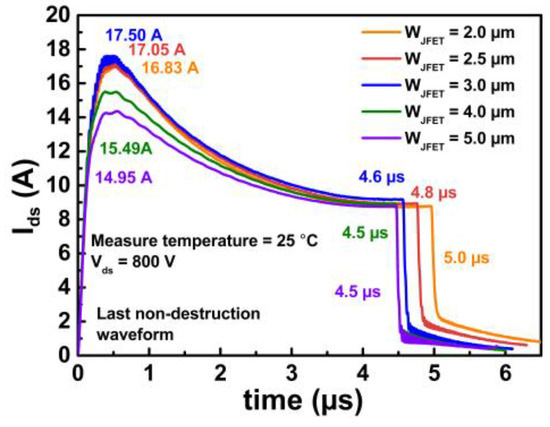
Figure 16. The SC current waveforms of five types of devices with different JFET widths at Vds = 800 V.
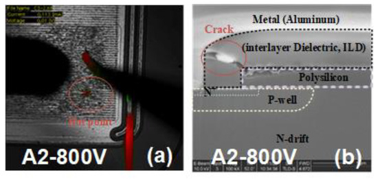
Figure 17. (a) The hot spot is observed under OBIRCH (Optical Beam Induced Resistance Change) of Device A2 at drain voltage of 800 V. (b) The cross-section at hot spot is prepared by FIB (Focus Ion Beam) of Device A2 at drain voltage of 800 V.
The SCWT tested under different bus voltages is summarized in Figure 18a. The energy can be calculated using short-circuit current waveforms and device voltage waveforms. The calculated results are plotted in Figure 18b. Devices with different JFET widths have almost the same SCWT under drain voltages of 600 and 800 V. The WJFET has a significant effect on the SCWT when the drain voltage is 400 V. For higher bus voltage conditions, the difference in SCWT among the five designs is significantly reduced.
In addition, at higher bus voltages, the maximum short-circuit energy that device can safely dissipate is reduced to 33%, as shown in Figure 18b. This is because the short-circuit current multiplied by a high bus voltage generates a significant amount of heat on a very short time scale (<1 μs), causing the device junction temperature to rise rapidly. Thus, the SCWT and total energy are decreased.
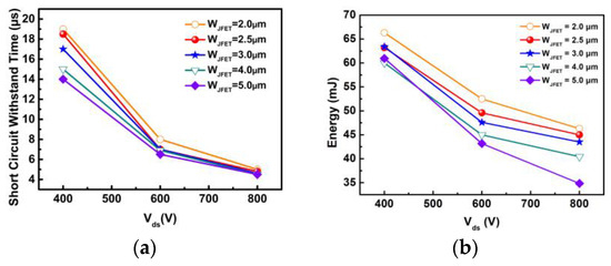
Figure 18. (a) The SCWT of five types of devices with different JFET widths. (b) The SC energy of five types of devices with different JFET widths.
4. Discussion
The on-resistance and short-circuit withstanding time are crucial parameters for SiC MOSFETs, representing their conduction performance and reliability, respectively. It has been reported that the structure designs (JFET region width in this work) can influence both the on-resistance and short-circuit withstanding time. Furthermore, there exists a trade-off relationship between the on-resistance and SCWT, which will be discussed in this section. Figure 19 summarizes the on-resistance and SCWT parameters for each device (Device A1–A5 with different WJFET designs).
The SCWT test results for the three bus voltage conditions (400, 600 and 800 V) are also illustrated in the figure. For each bus voltage, increasing the WJFET from 2 to 3 μm results in a decrease in device on-resistance from 1.68 to a minimum of 1.48 Ω (a reduction of 11.9%). However, a further increase in WJFET will raise the on-resistance, which is unacceptable. On the other hand, observing the SCWT parameters for the 400 V bus voltage condition (red lines in Figure 19), we can observe a slight drop from Device A1 to A3 (11.7%), followed by a significant drop from A3 to A5 (35.2%). The impact of WJFET designs on SCWT is negligible for higher bus voltages.
The bus voltage is usually determined by the power electronic system and circuit designs in practical applications. The saturation current primarily indicates the short-circuit current. The short-circuit current and saturation current are positively correlated. In SiC MOSFETs, the saturation current is influenced by two factors: the JFET region’s pinch-off voltage and the MOSFET channel’s saturation voltage. Short-circuit simulations are used to evaluate the potential under the gate oxide. With a wider JFET width, the potential at the JFET side increases, leading to an increase in channel saturation current due to the Drain-Induced Barrier Lowering effect.
Additionally, a lower pinch-off voltage results in a smaller saturation current in the JFET region. When the JFET region becomes sufficiently narrow, the saturation current of the JFET region becomes the primary factor. For 1200 V–rated SiC MOSFETs, the bus voltage can be selected between 400~800 V or even out of this range. In conclusion, the optimal design of WJFET is 3 μm for the 1200 V SiC MOSFETs studied in this work, without considering an enhanced doping concentration for the JFET region.
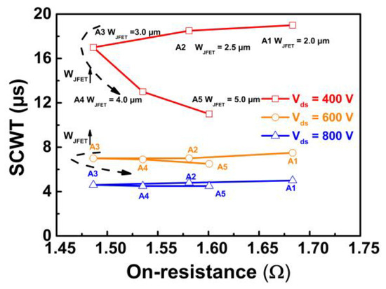
Figure 19. The relationship between on-resistance and SC withstanding time (SCWT) of different devices with varied JFET width.
Under high bus voltage conditions, devices with various JFET widths exhibit similar short-circuit behavior. As the JFET region becomes depleted during the short-circuit test, the resistances in the JFET region become relatively small compared to the channel resistance. Therefore, the JFET width has less impact on the result. Furthermore, it can be concluded that the variation in JFET width is not highly sensitive to the short-circuit withstand capability under high bus voltage, but it exhibits a greater impact under low bus voltage conditions. Moreover, Device A3 demonstrates the best performance within the voltage range of 400 to 800 V.
The relationship between the short-circuit test results at temperatures of 25 and 100 °C and the on-resistance under a 400 V bus voltage is shown in Figure 20 and will be discussed in the following paragraphs. In Section 3.2, the failure reason for DUTs under a high-temperature SC test is clarified. Failure mode is summarized in Figure 21. The failure of a wide WJFET device is due to gate oxide burnout tested in SC under room temperature. As the temperature increases, the failure mode changes to the ILD crack.
When the temperature is above 100 °C, the device failure mode becomes the same. When evaluating the performance of devices operated at high temperatures, the static resistance gradually increases with temperature, while the short-circuit duration time at high temperatures varies. The devices with wider WJFET inhibit the injection of hot electrons at an elevated temperature, thereby reducing the formation of defects caused by hot carriers.
Therefore, there is an improvement in SCWT. When the width of the JFET is less than 3.0 μm (A3), due to the increase in the junction temperature in the high-temperature test, the temperature in the interlayer dielectric reaches the critical value faster, resulting in a reduction in the short-circuit withstand time. If the temperature rises to 150 °C, the SCWT for WJFET devices may all decrease due to the failure mode being changed to the ILD crack mode.
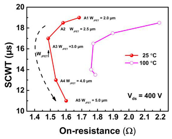
Figure 20. The relationship between on-resistance and SC withstanding time (SCWT) of devices with varied JFET width at 25 and 100 °C.
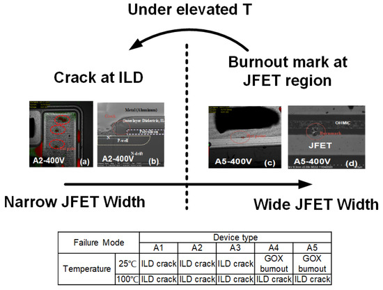
Figure 21. Summary of the failure mode of devices with different WJFET.
Judging from the trade-off relationship between the on-resistance and short-circuit current at room temperature and high temperature, devices with WJFET larger than 3.0 μm are more suitable for operating at high temperatures. These devices exhibit a gradual increase in resistance at high temperatures, resulting in an improved short-circuit performance to a certain extent.
5. Conclusions
In this paper, 1200 V SiC MOSFETs with various WJFET are fabricated, followed by a comprehensive comparison and study of the short-circuit robustness of these devices. Devices with narrow and wide WJFET exhibit distinct failure mechanisms. The ILD crack is observed in the device with narrow WJFET, while the breakdown of gate oxide is found in the device with wider WJFET after device failure. The relationship between on-resistance and SCWT of devices A1–A5 with different JFET widths is summarized.
Device A3 demonstrates the best performance in terms of SCWT and on-resistance characteristics, making it an improved design. Furthermore, devices with narrowed JFET widths have limitations in improving SCWT (<20 μs) under a bus voltage of 400 V. The relationship between the short-circuit test results at temperatures of 25 and 100 °C and on-resistance under a bus voltage of 400 V is also investigated. Devices with WJFET larger than 3.0 μm exhibit improved SCWT under high temperatures and are better suited for high temperature operation. As the temperature rises, their resistance shows a slow increment, contributing to an enhanced short-circuit performance to a certain degree.
Authors
Hongyi Xu, Baozhu Wang, Na Ren, Hu Long, Kai Huang and Kuang Sheng
Original – MDPI
-
LATEST NEWS / PRODUCT & TECHNOLOGY / Si2 Min Read
Alpha and Omega Semiconductor Limited (AOS) announced the release of its state-of-the-art automotive TO-Leadless (TOLL) package for the company’s automotive grade 80V and 100V MOSFETs. AOS’s TOLL package is developed to optimize the company’s power semiconductors as essential components in the evolution of e-mobility such as 2- and 3-wheel and other light vehicles. This new package helps designers meet the ongoing trend to electrify vehicles with the latest battery technology to meet clean energy zero-emission goals.
These capabilities make AOS 80V and 100V MOSFETs ideally suited for automotive BLDC motor and battery management applications for e-mobility. The AOS automotive TOLL package is designed to achieve the highest current capability using AOS’s innovative approach which utilizes advanced clip technology to achieve a high in-rush current rating.
In addition, AOS TOLL packaging with clip technology offers a very low package resistance and inductance, enabling improved EMI performance compared to other TOLL packages utilizing standard wire-bonding technology. With the combination of low ohmic and high current capability, utilizing AOS TOLL packaging also allows designers to reduce the number of parallel MOSFETs in high current applications. This, in turn, helps to enable higher power density requirements without compromising reliability in applications where robustness and reliability are key design objectives.
Providing a more compact solution for space-constrained designs, the AOTL66810Q (80V) and AOTL66912Q (100V) have a 30 percent smaller footprint compared to a TO-263 (D2PAK) package. These new devices in TOLL packaging are qualified to AEC-Q101, PPAP capable, and are manufactured in IATF 16949 certified facilities making them ideally suited for demanding application requirements in e-mobility. AOS TOLL devices are also compatible with automated optical inspection (AOI) manufacturing requirements.
“Using the AOS Automotive TOLL package with clip technology offers significant performance improvements in a robust package. The advanced technologies in our AOTL66810Q and AOTL66912Q MOSFETs will help simplify new designs allowing them to reduce the number of devices in parallel while providing the necessary higher current capability to enable overall system cost savings,” said Peter H. Wilson, Marketing Sr. Director of MOSFET product line at AOS.
Part Number VDS (V) VGS (±V) Continuous Drain Current (A) Pulsed Drain Current (A) RDS(ON) Max (mOhms) @10V @25°C @100°C @25°C AOTL66810Q 80 20 445 247 1780 1.25 AOTL66912Q 100 20 370 269 1480 1.7 Original – Alpha and Omega Semiconductor
