-
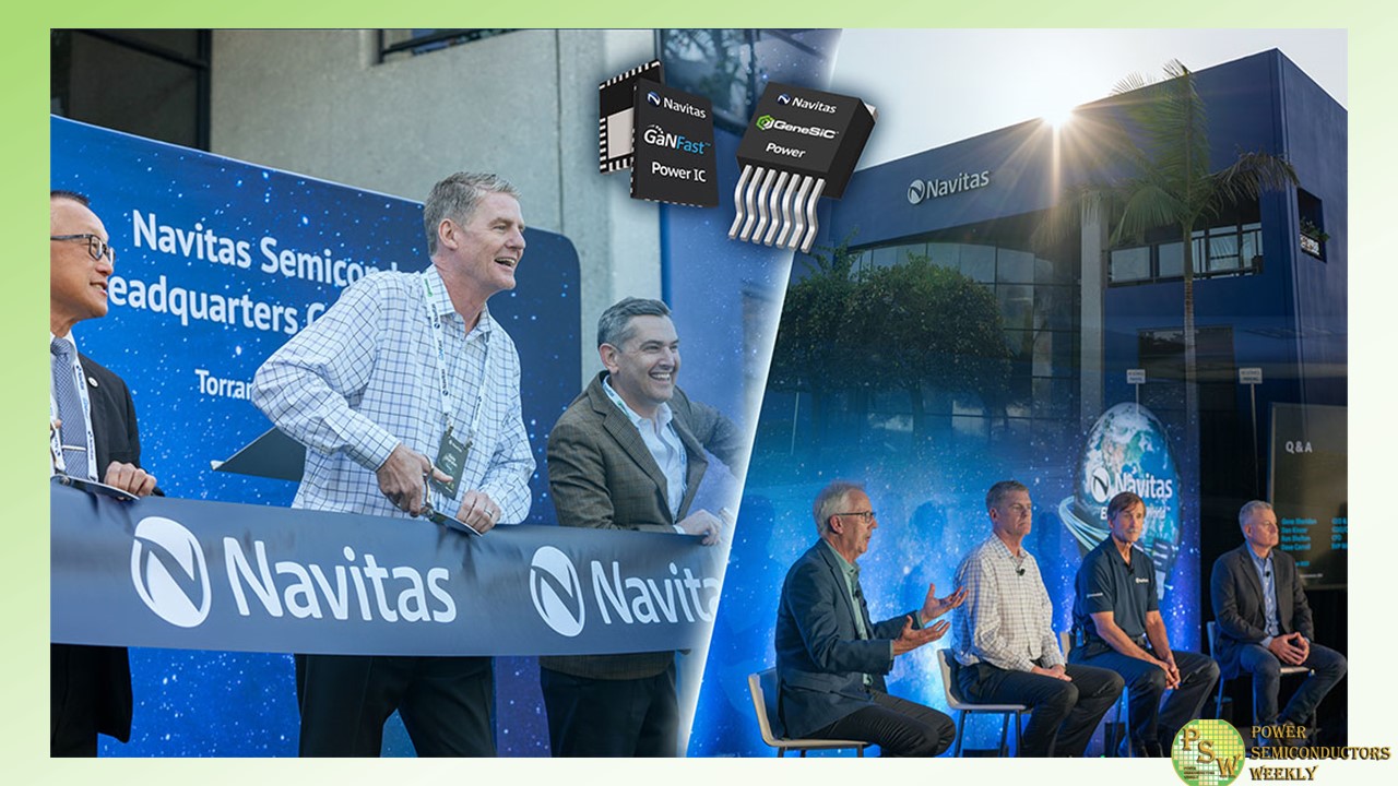
Navitas Semiconductor held an Opening Ceremony and 2023 Investor Day at its new headquarters in Torrance, CA.
Torrance Mayor, George Chen, and Dustin McDonald from the Office of the Governor of California joined Navitas’ CEO and co-founder Gene Sheridan to speak and cut the ribbon, officially opening Navitas’ new headquarters. Around 100 highly-skilled Navitas staff are employed in Torrance for all aspects of GaN and SiC design, applications, test, characterization and quality plus finance, marketing and HR. Further team growth is planned for 2024, including a $20M investment to add SiC epi-growth capability for strategic manufacturing expansion.
The well-attended investor meeting began with Mr. Sheridan’s recap on a year of significant growth for Navitas, with a doubling of revenue, a $92M capital raise, four major new technology platforms and an update on Navitas’ mission to ‘Electrify Our World™. Then, Mr. Sheridan outlined a $1.3T electrification market opportunity as GaN and SiC enable and accelerate our transition away from fossil fuels to a carbon-neutral, full-electrified world, envisaged as ‘Planet Navitas’.
Dan Kinzer, co-founder and COO/CTO then introduced technology platforms including Gen-4 GaNSense half-bridges for motor drive and mobile fast chargers, GaNSafe – the world’s most protected GaN powertrain, GaNSense Control, and a revolutionary new bi-directional GaN power IC platform with up to 9x smaller chip size than legacy silicon MOSFETs or IGBTs. Sid Sundaresan, SVP for the GeneSiC product line added more detail on the Gen-3 Fast SiC platform.
In May, Navitas announced a qualified customer pipeline of $760M, across mobile, solar/ESS, EV/eMobility, data center and appliance/industrial markets. At the Investor Day, David Carroll, SVP Worldwide Sales announce that the pipeline had increased by 65% to $1.25B, with 10/10 top mobile OEMs and majority of solar inverter makers. Investors also heard from the voices of Navitas customers, including Rick Liu from Accopower for EV, Belkin’s Steve Malony for mobile, Philipp Guo from VREMT for EV, Adam Weissman from Anker for mobile, and Harron Inam from DG Matrix for EV roadside charging.
Ron Shelton, Navitas CFO, presented more detail on the impressive financial results with increased gross margin, and over $170M is cash and no debt, plus a long-term target to grow 6x-10x more than the market, with 50%+ gross margins.
In-person visitors then toured the Navitas facility, including past & present demos and the ‘Electrify Studio’ experience – where Navitas is creating a vision for our electrified planet – plus SiC design, GaN IC design, applications, test & characterization, quality & reliability.
The day concluded with a celebration at the Crypto.com Arena, where guests enjoyed the LA Clippers’ victory—a fitting finale to a day filled with inspiration, innovation, and collaboration.
Comprehensive Investor Day material is available via the Navitas website, with presentation slides, and complete video playback of the main presentations, customer testimonials, and facility tour.
Original – Navitas Semiconductor
-
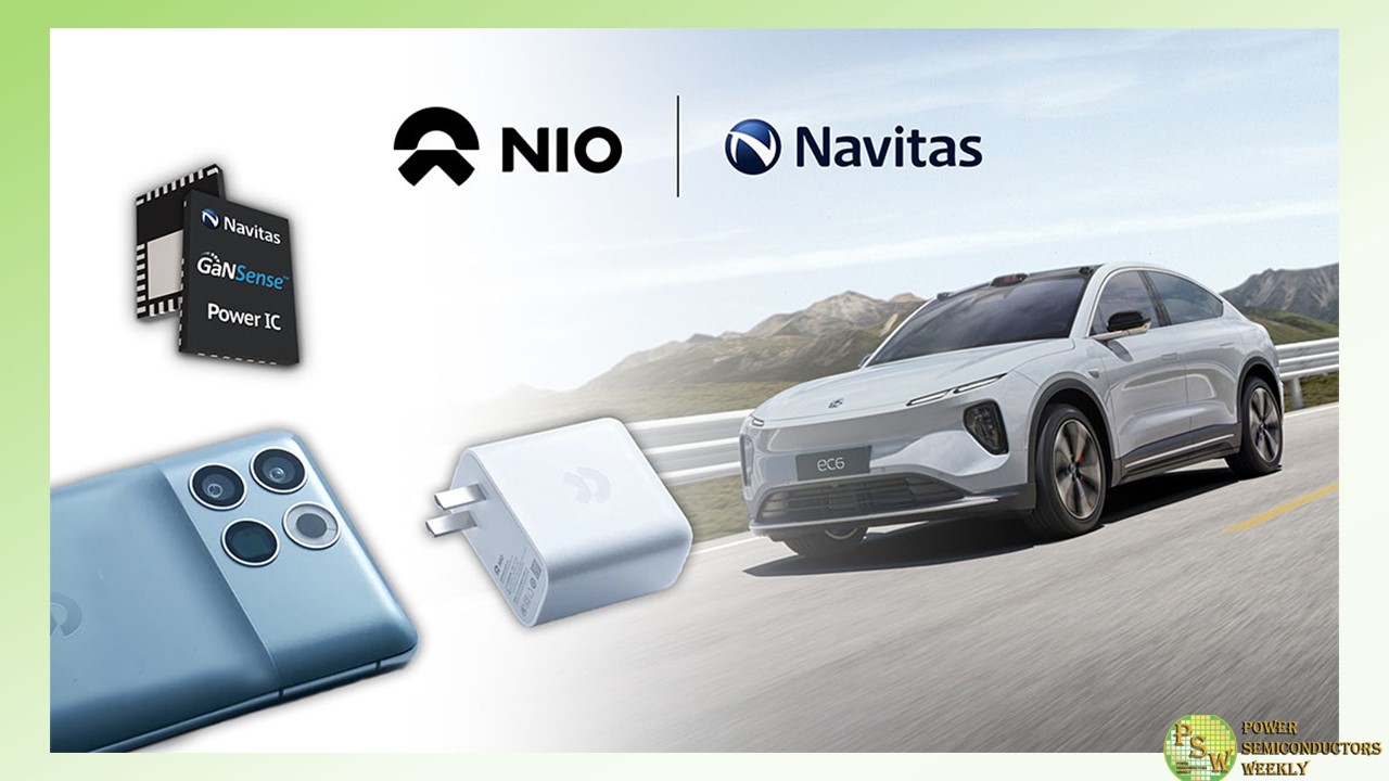
Navitas Semiconductor announced that NIO, a global, leading, new-energy vehicle maker has released its inaugural smartphone, the NIO Phone with a powerful 66 W fast charger featuring Navitas’ next-generation gallium-nitride (GaN) GaNFast™ power ICs equipped with GaNSense™ technology. This enhancement delivers flagship-level charging efficiency, providing end users with a better vehicle-centric mobile interconnection experience. New GaNFast ICs are replacing legacy silicon chips to enable next-gen fast-charging for mobile phones, tablets and laptops.
The flagship NIO Phone features the leading Qualcomm Snapdragon 8 Gen 2 chip, and boasts a 6.81-inch 2K variable refresh-rate curved screen, with the main, ultra-wide-angle, and 50 M pixel periscope telephoto cameras. Using NIO Link panoramic-interconnection technology, the NIO Phone integrates smoothly and seamlessly with smart EVs and NIO’s in-car system. With a single click, the driver can control over 30 functions, and equipped with ultra-wideband technology, it can completely replace traditional car keys.
To support such powerful and comprehensive features, the NIO Phone is equipped with a large 5,200 mAh battery and an in-box GaNFast charger offering up to 66 W of charging power. Measuring only 57 x 57 x 30 mm (97.5 cc), the NV6136 GaNFast power IC in a high-frequency quasi-resonant (HFQR) topology with loss-less current sensing and ultra-fast autonomous short-circuit protection, delivers power density of 1.03 W/cc.
Mr. Zhang Baozhou who is responsible for NIO’s mobile phone supply chain, stated, “NIO is dedicated to providing users with high-performance smart electric vehicles and ultimate user experience, creating a delightful lifestyle for our users.
The NIO Phone fulfills the expectations and needs of NIO users for a flagship smartphone, making their cars more intuitive and user-friendly. In launching NIO Phone, we are very pleased to collaborate with Navitas Semiconductor, industry leader in GaN to utilize the mature, cutting-edge GaNFast power ICs, allowing our users to experience a comprehensive, lightweight, and efficient charging experience.”
Mr. Wu Gongli, GM of R&D for TenPao, the manufacturing partner for the NIO Phone commented, “We are excited to work with Navitas to build this leading GaN charger for NIO users, marking an important milestone in TenPao’s development. Navitas’ GaNFast ICs deliver top power-density performance with easy-to-use features. The combination of high efficiency and fast design accelerates our time-to-market.”
Mr. Yingjie (Charles) Zha, VP and GM of Navitas China, stated, “Navitas is extremely honored to collaborate with TenPao to make the NIO Phone possible by integrating the leading GaNFast technology into the NIO Phone. Navitas’ mission to ‘Electrify Our World™’ aligns closely with NIO’s objective of ‘Blue Sky Coming’. This is just the beginning of our collaboration. In the future, Navitas will spare no effort to deeply-integrate energy-saving, sustainable, world-leading GaN and SiC technology into NIO Phone’s DNA, creating a comprehensive lifestyle revolution from a smartphone to EVs.”
Original – Navitas Semiconductor
-
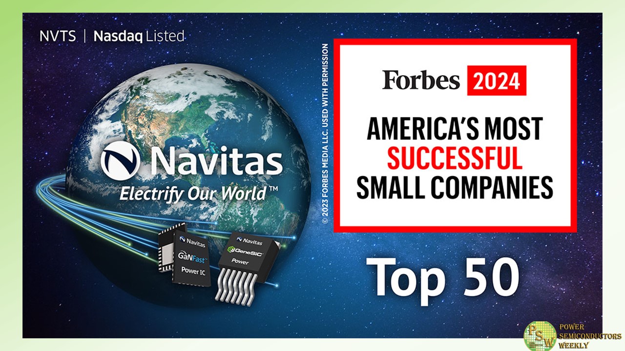
Navitas Semiconductor secured the 49th position on Forbes’ 2024 America’s Successful Small Companies list. The ranking is recognition of the company’s growth based on strong demand for Navitas’ advanced, high-efficiency, wide bandgap (WBG) GaN and SiC power components, across growing and diverse global markets and an expanding customer base.
Forbes evaluated Navitas on earnings growth, sales growth, return on equity, and total stock return over the preceding five years, with a specific focus on the last 12 months, including Navitas’ 115% increase in revenue (Q3’22 to Q3’23).
Looking ahead, Navitas will host an in-person 2023 Investor Day at the company’s new Torrance HQ (with livestream), from 12:30 pm Pacific / 3:30 pm US Eastern on Tuesday 12th December. Highlights include a deep dive into four major new GaN/SiC technology platforms and focus markets, plus customer testimonials and a refresh on the $1B+ customer pipeline, plus 2024 and long-term financial outlook.
“The top 50 ranking is great recognition by Forbes for Navitas’ growth,” said Gene Sheridan, co-founder and CEO. “GaN and SiC are accelerating the transition away from fossil fuels to ‘Electrify Our World™’ with renewable sources and efficient uses of electricity. This disruptive, displacement technology upgrades from legacy silicon chips, to make existing applications more efficient, lighter, faster charging and longer range, with lower system costs.”
Original – Navitas Semiconductor
-
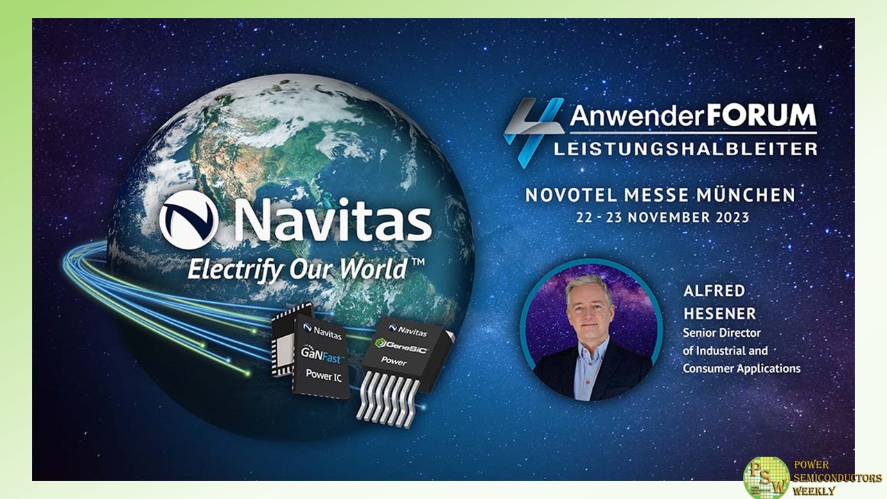
Navitas Semiconductor announced its participation in the Power Semiconductor User Forum, organized by WEKA Fachmedien on November 22nd -23rd, 2023. The event offers valuable insights into power electronics for developers and technical buyers.
Alfred Hesener, Senior Director of Industrial and Consumer Applications will explore “Reliability and Cost-of-Ownership Optimization in Industrial Power Supplies,” on November 23rd at 1:45 p.m. CET. Mr. Hesener will highlight next-generation solutions that achieve high power densities, cool operation, robust performance using Navitas’ GaNSense single and Half-Bridge power ICs.
Navitas’ GaNFast power ICs integrate GaN power and drive with control, sensing, and protection to enable faster charging, higher power density, greater energy savings and system cost reduction. In addition, each GaN power IC saves over 4 kg CO2 due to higher efficiency and dematerialization. New ‘Gen-3 Fast’ GeneSiC MOSFETs have up to 50% improved performance vs. other SiC devices, and save over 40 kg CO2 per unit vs. legacy silicon IGBTs.
“For industrial power designers, the WEKA forum highlights leading-edge, reliable technology for drives, pumps, chargers and power conversion, using GaN and SiC,” said Mr. Hesener. “Features like loss-less current sensing, programmable dV/dt, 2 kV ESD protection and autonomous sensing and protection are key enablers, and reduce time to market.”
WEKA Fachmedien’s Power Semiconductor User Forum 2023 will be held from November 22nd-23rd at the Novotel Messe Munich, Willy-Brandt-Platz 1, 81829 München, Germany.
Original – Navitas Semiconductor
-
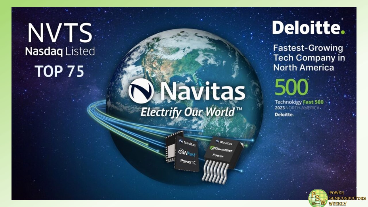
Navitas Semiconductor has announced that the company has been ranked 72nd on this year’s North American Deloitte Technology Fast 500™. This is the second year running that Navitas has been featured, improving from 75th to 72nd place, with increased revenue driven by strong demand for its advanced, high-efficiency, wide bandgap (WBG) gallium nitride (GaN) and silicon carbide (SiC) power components, across a growing number of global markets and customers.
Now in its 29th year, the Deloitte Technology Fast 500 is an independent ranking of the 500 fastest-growing technology, media, telecommunications, life sciences, fintech, and energy tech companies in North America. Based on percentage fiscal year revenue growth from 2019 to 2022, Navitas achieved 2,129% growth as GaN and SiC technology enabled efficient, sustainable applications and displaced legacy silicon chips.
Commenting on this year’s ranking, Navitas founder and CEO Gene Sheridan stated: “Our next-gen power-semi technologies are creating significant growth opportunities as we displace silicon in existing multi-$B markets like data centers, consumer, appliance and mobile applications. They also enable new-energy markets that are adopting GaN and SiC from the start, like EV, energy storage and renewable segments.
When combined, the growth results are extraordinary, and we appreciate the recognition of the Deloitte Fast 500 listing. We have built a strong foundation for further growth with established 3x-5x capacity increases, technology generational upgrades every 12-18 months, and a customer-focused, complete power-system design center approach, for applications from 20 W to 20 MW addressing a $22B per year opportunity.”
Original – Navitas Semiconductor
-
Navitas Semiconductor Corporation announced unaudited financial results for the third quarter ended September 30, 2023.
“I am pleased to announce another record quarter for Navitas as our gallium nitride and silicon carbide technologies continue to displace legacy power silicon in traditional markets and enable and accelerate new energy markets,” said Gene Sheridan, CEO and co-founder. “It’s a very exciting time at Navitas as we launch four major new technology platforms across GaN and SiC. We expect Navitas’ revenues to far exceed market growth rates in 2024 and for years to come.”
Financial Highlights
- Revenue: Total revenue grew to $22.0 million in the third quarter of 2023, a 115% increase from $10.2 million in the third quarter of 2022 and a 22% increase from $18.1 million in the second quarter of 2023.
- Gross Margin: GAAP gross margin for the third quarter of 2023 was 32.3%, impacted by inventory adjustments, compared to 3.8% in the third quarter of 2022 and 41.5% for the second quarter of 2023. Non-GAAP gross margin for the third quarter of 2023 was 42.1% compared to 38.4% for the third quarter of 2022 and 41.5% for the second quarter of 2023.
- Loss from Operations: GAAP loss from operations for the quarter was $28.6 million, compared to a loss of $37.4 million for the third quarter of 2022 and a loss of $27.2 million for the second quarter of 2023. On a non-GAAP basis, loss from operations for the quarter was $8.7 million compared to a loss of $10.3 million for the third quarter of 2022 and a loss of $9.6 million for the second quarter of 2023.
- Cash: Cash and cash equivalents were $176.7 million as of September 30, 2023.
Market, Customer and Technology Highlights
GaN is moving from a beachhead to the mainstream for mobile fast chargers, with continued strength and upside led by major China OEMs Xiaomi and Oppo. We expect 30% of their total mobile charger shipments in 2024 will utilize GaN, and GaN has been adopted by Samsung for the latest Galaxy S23 and other models, contributing to Q3 and expected Q4 2023 revenue ramp. New Gen-4 GaNSense™ half-bridge ICs, targeting ultra-fast chargers of 100 W or more, are projected to contribute another $10 million per year in revenue ramping in 2024. The new GaNSense products replace dozens of components with a single GaN IC and enable switching frequencies up to 2 MHz to reduce footprint and simplify designs.
Launched in September, GaNSafe™ is the world’s most-protected, most-reliable and highest-performance GaN power semiconductor, with advanced sensing, protection, higher-power capability and cool operation. GaNSafe breaks the glass ceiling for GaN to enter high-power, high-reliability markets like AI data centers, solar, EV and industrial. GaNSafe power ICs are featured in a new 6.6 kW, 800 V on-board charger (OBC) platform from Navitas’ dedicated EV system design center, setting industry benchmarks in system efficiency, density and cost, and attracting significant customer interest. The OBC is a ‘hybrid’ platform, featuring GaNSafe and a new, Gen-3 Fast (G3F) GeneSiC™ MOSFET platform, with leading-edge silicon carbide power and switching performance up to 50% better than competition.
Rapid AI adoption has created unprecedented demand for more power, higher efficiency and greater power density. Navitas’ data center design center has developed a new 4.5 kW AC-DC system platform design, with efficiency exceeding the 96% ‘Titanium Plus’ standard, and with twice the power density of previous, best-in-class, legacy silicon designs. GaNSafe and Gen-3 Fast SiC are again used to optimize these high-power applications, with significant growth in the number of customer pipeline projects.
Solar, appliance and industrial markets also show robust growth in the customer pipeline, with broad interest in the new Gen-3 Fast MOSFETs. The Gen-4 GaNSense half-bridge portfolio now includes new application-specific ICs for motor drives, compressors and pumps up to 1 kW, with sensing, autonomy and programming functionality for easy EMI.
Q4 2023 will also see the introduction of a new, breakthrough innovation: ‘bi-directional’ GaN. Each GaN power IC will replace up to four discrete power transistors, dramatically reducing component count, cost and complexity, and delivering major speed and efficiency benefits. Bi-directional GaN technology is expected to usher in major advances in energy storage, grid infrastructure, motor drives and many other emerging topologies and architectures across multiple markets.
Business Outlook
Fourth quarter 2023 net revenues are expected to increase to $25.0 – $26.0 million. Gross margin for the fourth quarter is expected to expand to 42.5%, plus or minus 30 basis points, and operating expenses, excluding stock-based compensation and amortization of intangible assets, are expected to be approximately $20.0 million in the fourth quarter of 2023. Weighted-average basic share count is expected to be approximately 179 million shares for the fourth quarter of 2023.
Original – Navitas Semiconductor
-

Navitas Semiconductor announced another GaNFast win at Samsung, this time a new 25W charger for the flagship Galaxy S23 smartphone. Gallium nitride (GaN) is a next-gen power-semi technology that is replacing legacy silicon chips in markets from mobile and consumer to data center, solar and EV.
The high-spec Galaxy S23 features a Dynamic AMOLED 2X, 120Hz screen with 1750 nits peak contrast, stretching it’s 1080 x 2340 pixels across 90.1 cm2 of Corning Gorilla Glass. With a Qualcomm Snapdragon 8 Gen 2 chip, up to 512GB / 8GB RAM of storage and triple cameras up to 50 MP, the S23 excels in mobile communication performance.
For power, the S23 features a 3900 mAh Li-Ion battery, and with the GaNFast 25W charger (model EP-T2510) with USB PD 3.0 interface, reaches 50% charge in only 30 minutes, and while in sleep mode, consumes only 5 mW of power. The PD 3.0 specification means that the new charger can power a range of devices from Galaxy Buds2 audio to Galaxy Z Fold5, Galaxy Flip and Galaxy A23.
Navitas’ GaNFast technology is used in a high-frequency, quasi-resonant (HFQR) topology running at 150 kHz. GaNFast leading-edge, high-frequency performance shrinks the charger by more than 30%, and the Navitas device is fully qualified to Samsung’s stringent qualification requirements, with excellent delivery performance, quality and reliability.
“As pioneers in mobile fast charging, Navitas continues to lead the next-gen market, with all 10 of the top 10 mobile OEMs in production with GaNFast products,” said David Carroll, Sr. VP Worldwide Sales. “From 25 W to 20 MW, our expanding range of leading-edge GaN and SiC products cover everything from mobile and consumer to EVs, solar and industrial applications.”
Original – Navitas Semiconductor
-
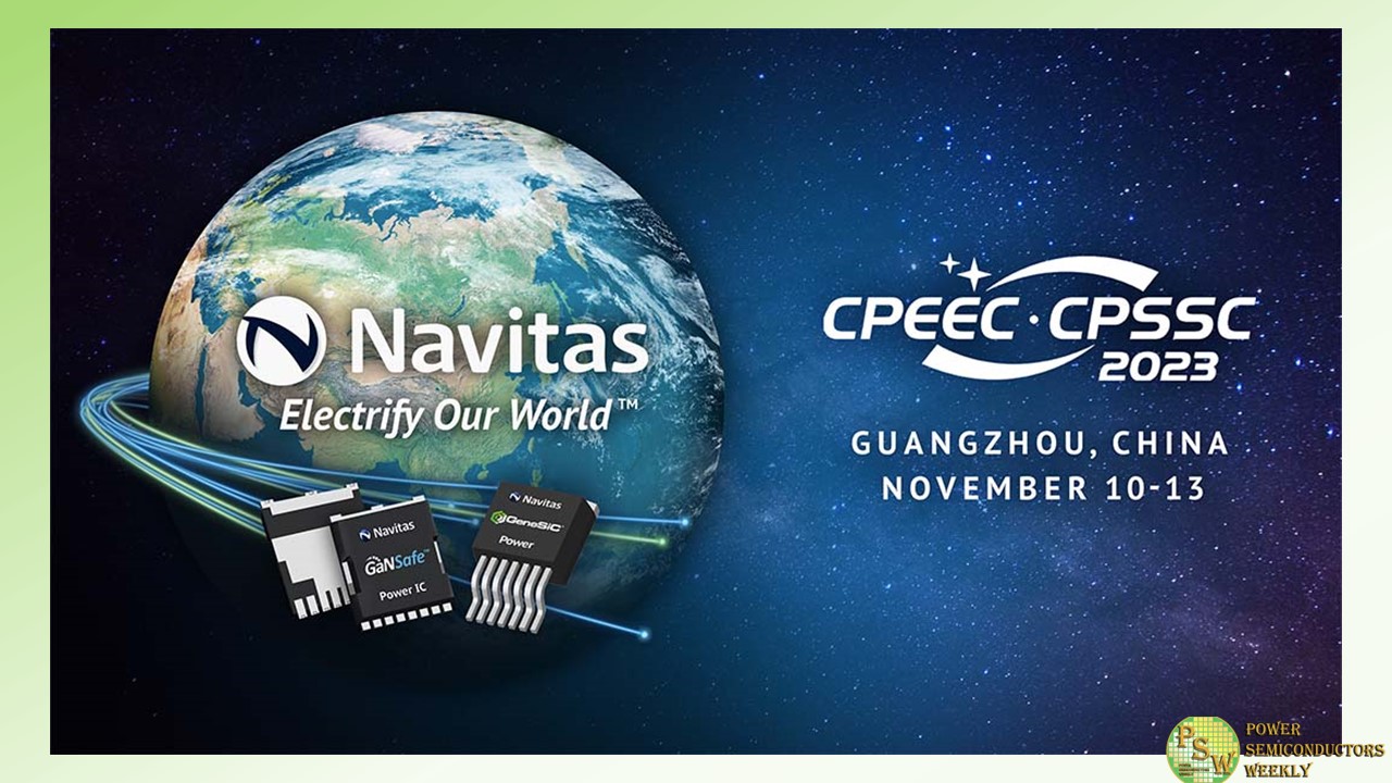
Navitas Semiconductor announced its continued sponsorship of the 2023 China Power Electronics and Energy Conversion Congress & the 26th China Power Supply Society (CPSS) Conference and Exhibition (CPSSC 2023), revealing major next-generation gallium nitride (GaN) and silicon carbide (SiC) power semiconductor platforms, including GaNSafe™ – the world’s safest GaN power semiconductor.
Hosted in Guangzhou from November 10th-13th, CPSSC 2023 celebrates its 40th anniversary and promotes academic and technical exchange in the fields of power electronics, energy conversion, and power technology, to foster technical innovation and related industries.
Navitas is the technology and market leader in GaN, with over 100 million GaNFast™ power ICs shipped, and over 12 million GeneSiC™ power MOSFETs and diodes shipped into a $22 billion per year total market opportunity.
With GaNSafe, Navitas has optimized its 4th-generation GaN technology for demanding, high-power applications in data centers, solar / energy storage and EV markets, where efficiency, power density and robust & reliable operation are critical. Adopting a novel, robust, and cool-running surface-mount TOLL package, GaNSafe integrates features and functions, including:
- Protected, regulated, integrated gate-drive control, with zero gate-source loop inductance for reliable high-speed 2 MHz switching to maximize power density.
- High-speed short-circuit protection, with autonomous ‘detect and protect’ within 50 ns – 4x faster than competing discrete solutions.
- Electrostatic discharge (ESD) protection of 2 kV, vs. zero for discrete GaN transistors.
- 650/ 800 V capability to aid survival during extraordinary application conditions.
- Easy-to-use, complete, high-power, high-reliability, high-performance power IC with only 4 pins, accelerating customer designs.
- Programmable turn-on and turn-off (dV/dt) to simplify EMI regulatory requirements.
Navitas’ CPSSC 2023 program includes comprehensive, in-depth technology, application and market presentations include a plenary keynote speech, full conference paper, four industrial sessions, a guest PSMA presentation, an in-depth 3.5-hour technology seminar and full GaNSafe launch. Visitors to the exhibition will discover ground-breaking technology demonstrations and complete power system platform designs at the Navitas booth.
Original – Navitas Semiconductor
-
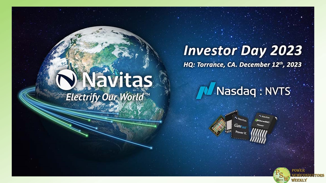
Navitas Semiconductor announced the 2023 Investor Day, to be held at the company’s new headquarters, on Tuesday 12th December, 2023.
Meeting highlights include:
- Four major new GaN/SiC technology platforms and five focus markets, including new GaNSafe technology, positioned to revolutionize AI-based data centers, EV, and renewable applications.
- Invited customer presentations, with leading-edge applications enabled by Navitas.
- $1B+ customer pipeline & what this means to Navitas growth trajectory, with a preview of 2024 forecast and long-term targets.
- Navitas’ unique, detailed view on the past, present and future of power electronics as we look to “Electrify Our World” (guided tour, and management small-group meetings).
For in-person attendance or participation virtually via live-stream, please contact ir@navitassemi.com
Original – Navitas Semiconductor
-
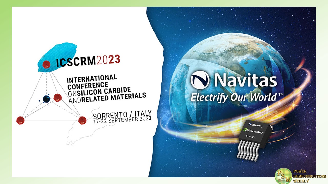
Navitas Semiconductor announced participation at the International Conference on Silicon Carbide and Related Materials (ICSCRM) 2023, to be held in Sorrento, Italy.
The ICSCRM conference fosters collaboration and knowledge sharing among the brightest minds in the field. The conference has a rich history dating back to its inaugural meeting in 1987, evolving into a premier global forum for in-depth technical discussions on all aspects of SiC and related materials.
GeneSiC™ power devices, optimized for high-power, high-voltage, and high-reliability SiC applications, address critical markets including electric vehicles, solar energy, energy storage, industrial applications, data centers, and consumer electronics. With an unmatched voltage range spanning from 650 V to 6.5 kV, GeneSiC MOSFETs and Schottky MPS™ diodes have been at the forefront of SiC technology advancement, offering performance and efficiency that pave the way for a more electrified and sustainable future.
Navitas Semiconductor will present two paper sessions at ICSCRM 2023:
- “New Generation SiC MPS Diodes with Low Schottky Barrier Height”
- “650 V SiC Power MOSFETs with Statistically Tight VTH Control and RDS(ON) of 1.92 mΩ-cm²”
Additionally, Navitas’ SVP of SiC Technology & Operations, Dr. Sid Sundaresan, will be chairing the session on Thursday, September 21st. The session, titled “Devices 4: Short circuit, avalanche and reliability,” will focus on crucial topics in the field of SiC technology.
“Navitas’ presence at ICSCRM 2023 is a testament to the company’s unparalleled expertise in SiC technology and its commitment to driving innovation in the industry,” said Dr. Ranbir Singh, Navitas EVP for the GeneSiC business line. “As a pioneer in the field, we continue to extend the boundaries of SiC technology, revolutionizing power semiconductors with cutting-edge GeneSiC™ technology.”
Original – Navitas Semiconductor
