-

The safe hot-swap operation in AI servers and telecom requires MOSFETs with a robust linear operating mode as well as a low R DS(on). Infineon Technologies AG addresses this challenge with the new OptiMOS™ 5 Linear FET 2, a MOSFET designed to provide the ideal trade-off between the R DS(on) of a trench MOSFET and the wide safe operating area (SOA) of a classic planar MOSFET.
The device prevents damage to the load by limiting the high inrush current and ensures minimal losses during operation due to its low R DS(on). Compared to the previous generation (the OptiMOS Linear FET), the OptiMOS Linear FET 2 offers improved SOA at elevated temperatures and reduced gate leakage current, as well as a wider range of packages. This allows for more MOSFETs to be connected in parallel per controller, reducing bill-of-material (BOM) costs and offering more design flexibility due to the extended product portfolio.
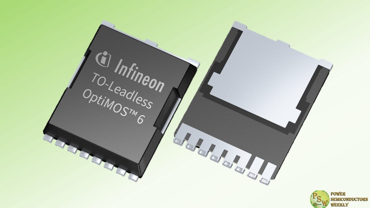
The 100 V OptiMOS 5 Linear FET 2 is available in a TO-leadless package (TOLL) and offers a 12 times higher SOA at 54 V at 10 ms and 3.5 times higher SOA at 100 µs compared to a standard OptiMOS 5 with similar R DS(on). The latter improvement is particularly important for the battery protection performed inside the battery management system (BMS) in case of a short circuit event. During such events the current distribution between parallel MOSFETs is critical for the system design and reliability.
The OptiMOS 5 Linear FET 2 features an optimized transfer characteristic that allows for improved current sharing. Taking into account the wide SOA and improved current sharing, the number of components can be reduced by up to 60 percent in designs where the number of components is determined by the short-circuit current requirement. This enables high power density, efficiency, and reliability for battery protection which are used in a wide range of applications including power tools, e-bikes, e-scooters, forklifts, battery back-up units and battery-powered vehicles.
The new OptiMOS 5 Linear FET 2 MOSFET is now available. Further information can be found at www.infineon.com/optimos-linearfet and www.infineon.com/ipt023n10nm5lf2.
Original – Infineon Technologies
-
Infineon Technologies AG expands its OptiMOS™ 6 MOSFET portfolio with the new 135 V and 150 V product families. The devices are designed to meet the requirements of drives and switched-mode power supply (SMPS) applications and complement the recently released launched OptiMOS 6 120 V MOSFETs.
With the extended portfolio, Infineon offers its customers a wide range of alternatives to select the best-fit MOSFETs for various applications. Lower switching losses benefit applications like server SMPS, solar optimizers, high-power USB chargers, and telecom. Improved conduction losses are highly beneficial for motor inverters in e-forklifts and light electric vehicles (LEVs).
Compared to the previous generation (OptiMOS 5 150 V MOSFETs), the new product families offer a reduction in on-state resistance R DS(on) of up to 50 percent, while the FOM g is reduced by 20%. With the very low R DS(on), their improved switching performance and excellent EMI behavior, both new families deliver unparalleled efficiency, power density, and reliability. A faster and softer body diode delivers an up to 59 percent lower Q rr, less overshoot and ringing.
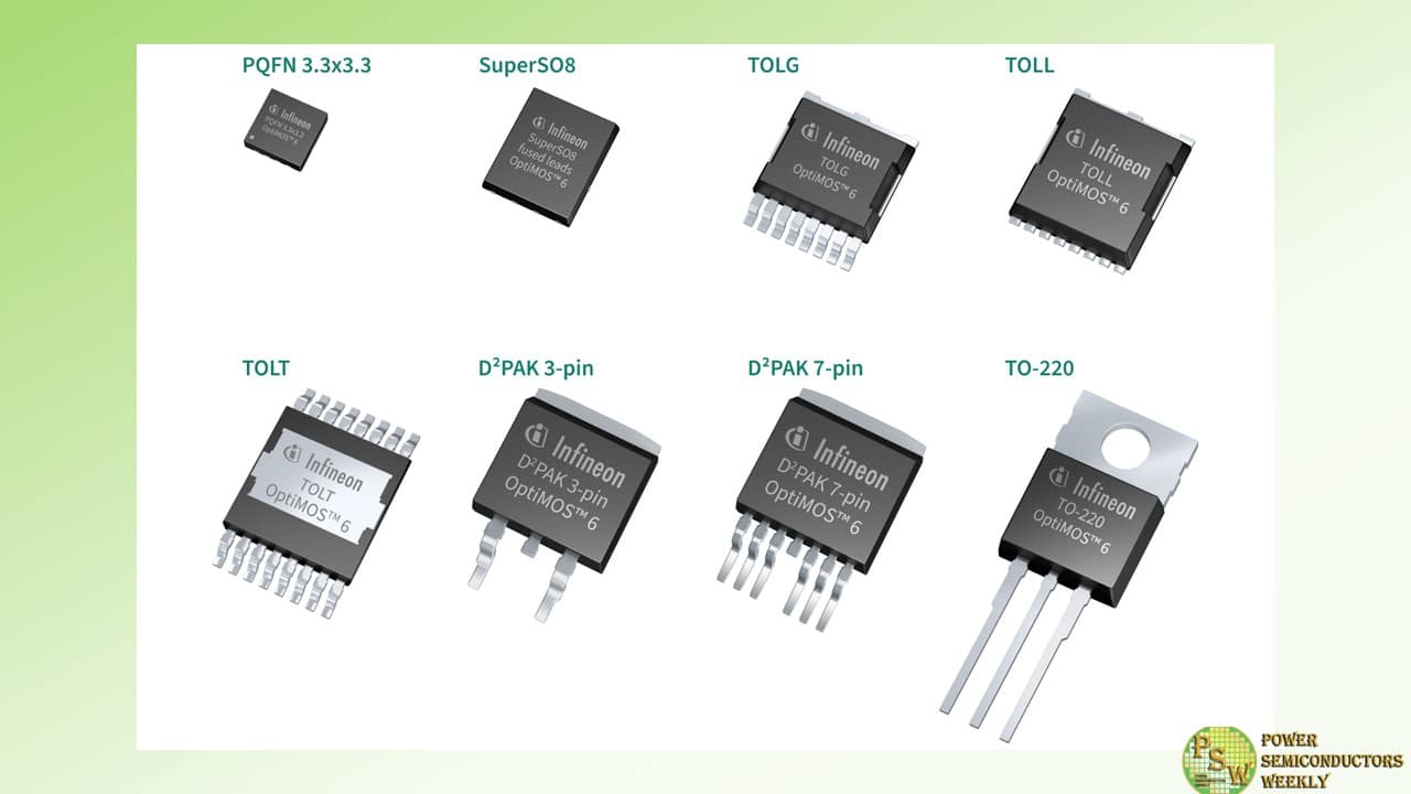
The OptiMOS 6 135 V and 150 V MOSFETs are available in a variety of packages to provide customers with a range of options for best-fit products. This broad package portfolio includes TO-220, D 2PAK 3-pin, D 2PAK 7-pin, TOLL, TOLG, TOLT, SuperSO8 5×6 and PQFN 3.3×3.3.
The OptiMOS 6 135 V and 150 V MOSFETs can be ordered now. Further information is available at www.infineon.com/optimos-6-135v and www.infineon.com/optimos-6-150v.
Original – Infineon Technologies
-
Infineon Technologies AG is expanding its portfolio of next-generation OptiMOS™ 7 MOSFETs for automotive applications: the portfolio of 40 V products now includes additional devices in robust, lead-free packages. In addition, 80 V and 100 V OptiMOS 7 MOSFETs are now also available.
The MOSFETs are optimized for all standard and future automotive 48 V applications, including electric power steering, braking systems, power switches in new zone architectures, battery management, e-fuse boxes, DC/DC, and BLDC drives in various 12 V and 48 V electrical system applications. They are also suitable for other transportation applications such as light electric vehicles (LEV), e2wheelers, eScooters, eMotorcycles, and commercial and agricultural vehicles (CAV).
“As a technology leader in power semiconductors, Infineon is committed to shape the future technology standards in automotive power MOSFETs in terms of power efficiency, innovative and robust power packaging with high quality,” said Axel Hahn, Senior Vice President and General Manager Automotive LV MOSFETs of Infineon. “We are providing our customers a diverse product portfolio and are addressing all their requirements to drive the development of modern automotive applications.”
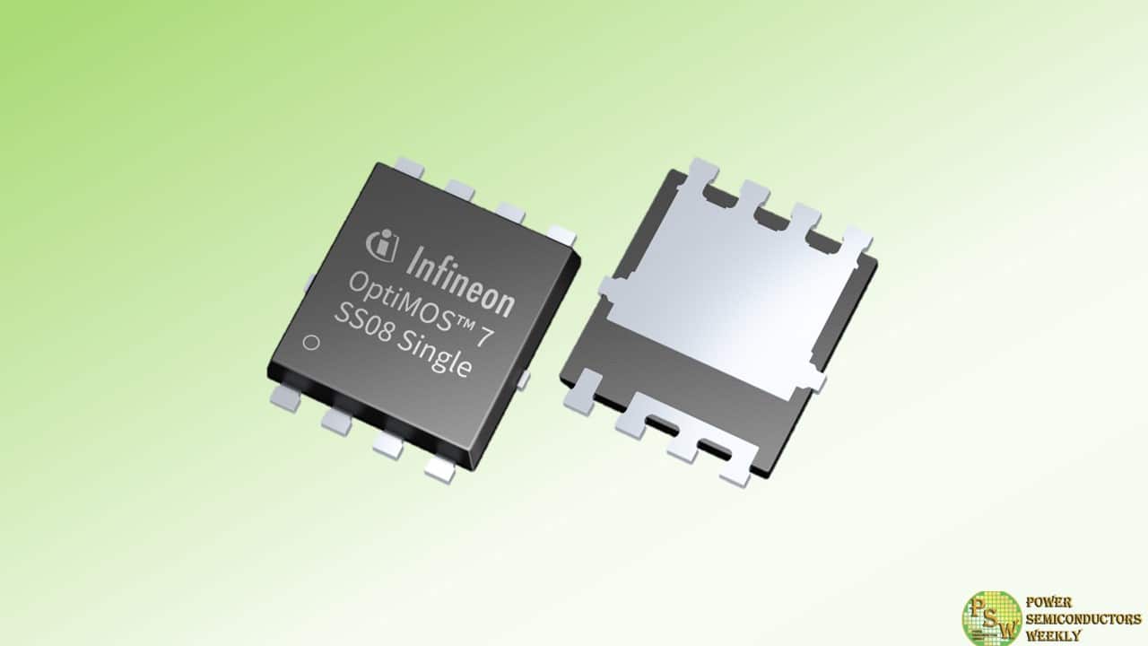
By combining 300 mm thin-wafer technology and innovative packaging, the new OptiMOS 7 technology enables significant performance advantages in all available voltage classes. As a result, the components are now available in various rugged automotive power packages, including Single SSO8 (5×6), Dual SSO8 (5×6), mTOLG (8×8) and sTOLL (7×8).
The family offers high power density and energy efficiency with the industry’s lowest on-state resistance (e.g. 1.3 mΩ max in a single SSO8 (5×6) 80V package) in the smallest form factor. The devices also offer reduced switching losses, improved Safe Operating Area (SOA) robustness and high avalanche current capability. With this, they enable a highly efficient system design for tomorrow’s automotive applications.
Original – Infineon Technologies
-
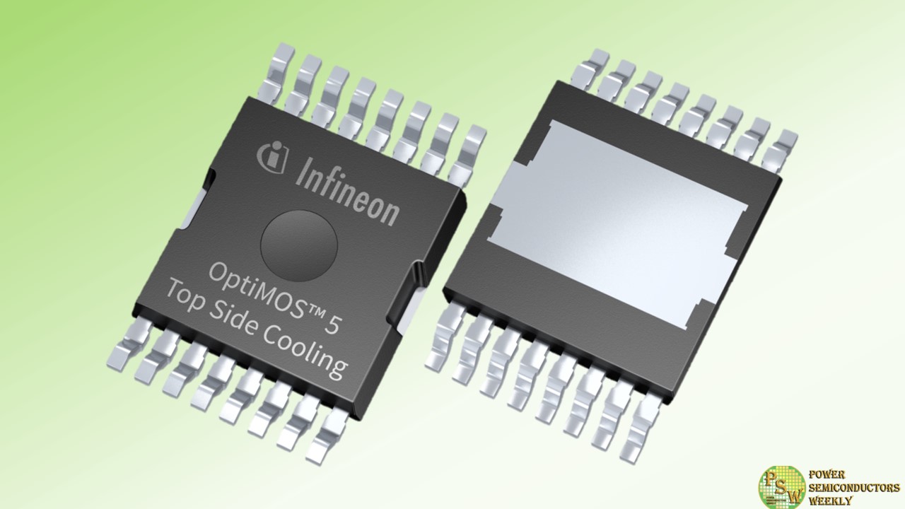
Infineon Technologies AG introduced the SSO10T TSC package with OptiMOS™ MOSFET technology. With its direct top-side cooling concept, the package offers excellent thermal performance. This eliminates heat transfer into or through the PCB of the automotive electronic control unit.
The package enables a simple and compact double-sided PCB design and minimizes cooling requirements and system costs for future automotive power designs. The SSO10T TSC is therefore well suited for applications such as electric power steering (EPS), EMB, power distribution, brushless DC drives (BLDC), safety switches, reverse battery, and DCDC converters.
The SSO10T TSC has a 5 x 7 mm² footprint and is based on the established industry standard SSO8, a 5 x 6 mm² robust housing. However, due to its top-side cooling, the SSO10 TSC offers more than 20 percent and up to 50 percent higher performance than the standard SSO8 – depending on the thermal interface (TIM) material used and the TIM thickness. The SSO10T TSC package is JEDEC listed for open market and provides wide second source compatibility. As a result, the package can be introduced quickly and easily as the future standard for top-side cooling.
The SSO10T package enables a very compact PCB design and reduces the system footprint. It also lowers the cost of the cooling design by eliminating vias, resulting in lower overall system costs and design effort. At the same time, the housing offers high power density and efficiency, thus supporting the development of future-proof and sustainable vehicles.
Original – Infineon Technologies
-
Motor drive applications are taking a leap forward with the launch of the Infineon Technologies AG OptiMOS™ 6 200 V MOSFET product family. The new portfolio is designed to deliver optimal performance in applications such as e-scooters, micro-EVs, and E-forklifts.
The improved conduction losses and switching behavior for these new MOSFETs reduce the electromagnetic interference (EMI) and switching losses. This benefits various switching applications, including servers, telecom, energy storage systems (ESS), audio, solar and others.
Additionally, the combination of a wide safe operating area (SOA) and industry-leading R DS(on) results in a perfect fit for static switching applications such as battery management systems. With the introduction of the new OptiMOS 6 200 V product family, Infineon sets a new industry benchmark with increased power density, efficiency, and system reliability for its customers’ benefit.
The OptiMOS 6 200 V portfolio delivers enhanced technical features compared to its predecessor, the OptiMOS 3. It features a 42 percent lower R DS(on) that contributes to reduced conduction losses and increased output power. Regarding diode behavior, the OptiMOS 6 200 V provides a significant increase in softness, more than three times that of the OptiMOS 3.
Combined with up to 89 percent reduction in Q rr(typ), the switching and EMI behaviors are significantly improved. The technology also features improvements in parasitic capacitance linearity (C oss and C rss), which reduces oscillation during switching and lowers voltage overshoot. A tighter V GS(th) spread and lower transconductance aid in MOSFET paralleling and current sharing, leading to more uniform temperatures and reducing the number of paralleled MOSFETs.
The OptiMOS 6 200 V products feature an improved SOA and are classified as MSL 1 according to J-STD-020. These RoHS-compliant, lead-free products align with current industry standards.
Original – Infineon Technologies
-
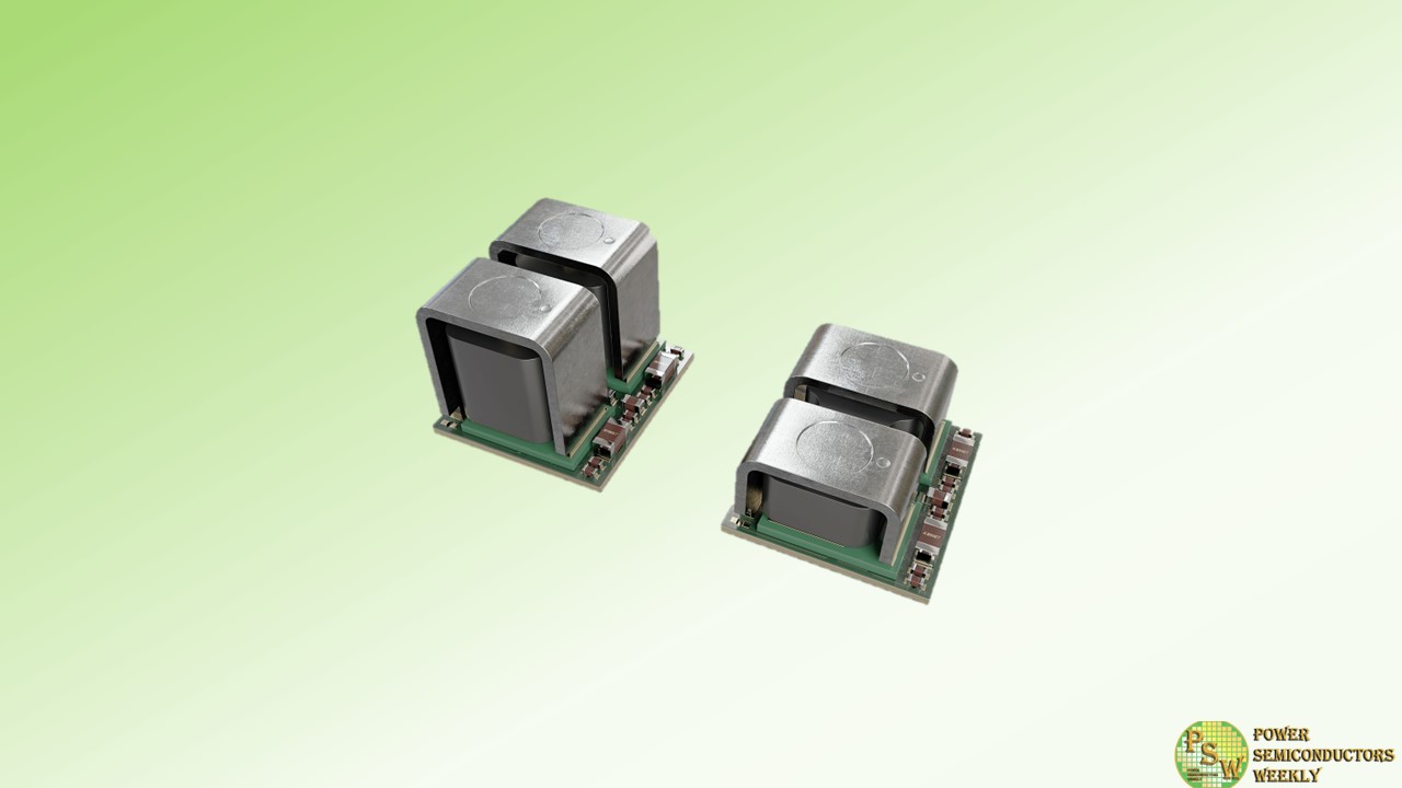
Artificial Intelligence is currently driving an exponential increase in global data generation, and consequently increasing the energy demands of the chips supporting this data growth. Infineon Technologies AG launched its TDM2254xD series dual-phase power modules that enable best-in-class power density, quality and total cost of ownership (TCO) for AI data centers.
The TDM2254xD series products blend innovation in robust OptiMOS TM MOSFET technology with novel packaging and proprietary magnetic structure to deliver industry-leading electrical and thermal performance with robust mechanical design. This lets data centers operate at higher efficiency to meet the high power demands of AI GPU (Graphic Processor Unit) platforms while also significantly reducing TCO.
Given that AI servers require 3 times more energy than traditional servers, and data centers already consume more than 2 percent of the global energy supply, it is essential to find innovative power solutions and architecture designs that further drive decarbonization. Paving the way for the green AI factory, Infineon’s TDM2254xD dual-phase power modules combine with XDP TM Controller technology to enable efficient voltage regulation for high-performance computing platforms with superior electrical, thermal and mechanical operation.
Infineon introduced the TDM2254xD series at the Applied Power Electronics Conference (APEC). The modules’ unique design allows for efficient heat transfer from the power stage on to the heat sink through novel inductor design that is optimized to transfer current and heat, thereby allowing for a 2 percent higher efficiency than industry average modules at full load. Improving power efficiency at the core of a GPU yields significant energy savings at scale. This translates into megawatts saved for data centers computing generative AI and in turn leads to reduced CO 2 emissions and millions of dollars in operating cost savings over the system’s lifetime.
“This unique Product-to-System solution combined with our cutting-edge manufacturing lets Infineon deliver solutions with differentiated performance and quality at scale, thereby significantly reducing total cost of ownership for our customers,” said Athar Zaidi, Senior Vice President, Power & Sensor Systems at Infineon Technologies. “We are excited to bring this solution to market; it will accelerate computing performance and will further drive our mission of digitalization and decarbonization.”
Original – Infineon Technologies
-
The electrification of the transportation system is advancing continuously. In addition to passenger cars, 2- and 3-wheelers as well as light vehicles are increasingly being electrified. Therefore, the automotive market for Electronic Control Units (ECUs) powered by 24 V-72 V is expected to keep growing in the coming years.
To address this development, Infineon Technologies AG is complementing its OptiMOS™ 5 portfolio of automotive MOSFETs in the 60 V and 120 V range with new products in the high power packages TOLL, TOLG and TOLT. They are offering a compact form factor with very good thermal performance combined with excellent switching behavior.
The six new products offer a narrowed gate threshold voltage (V GS(th)) enabling designs with parallel MOSFETs for increased output power capability. The IAUTN06S5N008, IAUTN06S5N008G and IAUTN06S5N008T are 60 V MOSFETs, and the IAUTN12S5N017, IAUTN12S5N018G and IAUTN12S5N018T are 120 V MOSFETs.
The on resistance (R DS(on)) ranges from 1.7 mΩ to 1.8 mΩ for the 120 V MOSFETs and is 0.8 mΩ for the 60 V MOSFETs. This makes the 60V MOSFETs perfectly suited for high power 24 V supplied CAV applications or for HV-LV DCDC converters in xEVs. The 120 V MOSFETs are used in 48 V – 72 V supplied traction inverters for 2- or 3-wheelers and light electric vehicles.
Original – Infineon Technologies
-
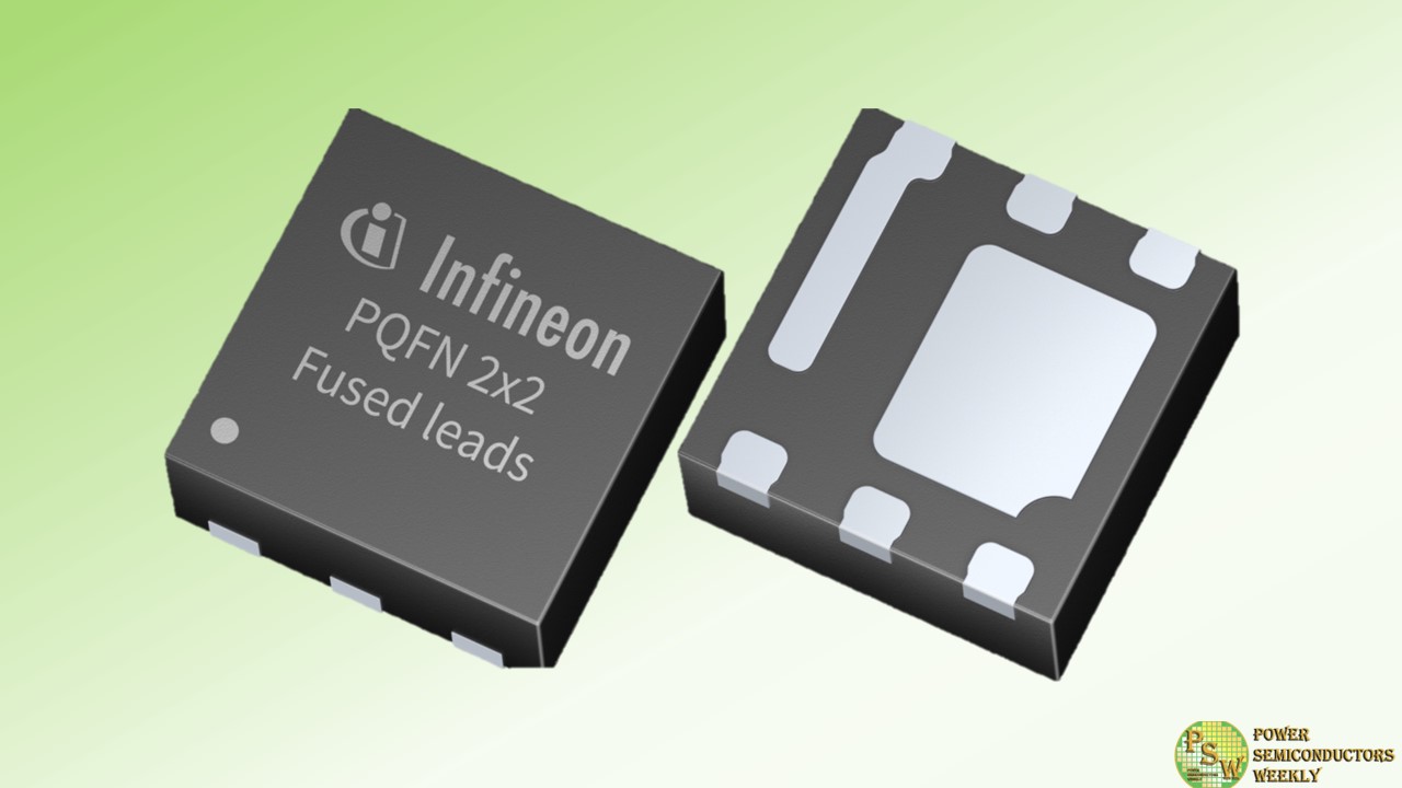
A small footprint of discrete power MOSFETs plays a critical role in achieving space savings, cost reduction, and easy-to-design applications. Additionally, higher power density can lead to layout routing flexibility and overall system size reduction. By expanding the current PQFN 2×2 portfolio with the new best-in-class OptiMOS™ power MOSFETs, Infineon Technologies AG offers benchmark solutions optimized for efficiency and performance in a small footprint. The new products are ideal for applications like synchronous rectification in switched mode power supplies (SMPS) for servers, telecom, and portable- and wireless chargers. Additional applications also include electric speed controllers for small brushless motors in drones.
The new OptiMOS 6 40 V and OptiMOS 5 25 V and 30 V power MOSFETs further optimize the proven OptiMOS technology for high-performance designs. They offer leading-edge silicon technology, package reliability, and superior thermal resistance (R thJC, max = 3.2 K/W) in the ultra-small PQFN 2×2 mm² package. The new devices combine industry-leading low on-resistance R DS(on) with industry-leading figures of merit (FOMs, Q G and Q OSS) for outstanding dynamic switching performance. As a result, MOSFETs with ultra-low switching and reduced conduction losses ensure optimal energy efficiency and power density, all while simplifying thermal management.
With the compact PQFN 2×2 mm² package outline, the OptiMOS power switches enable an improved system form factor with smaller, more flexible geometric outlines for end-user applications. The MOSFETs facilitate reliable system design with less need for paralleling, significantly reducing space and system cost.
Original – Infineon Technologies
