-

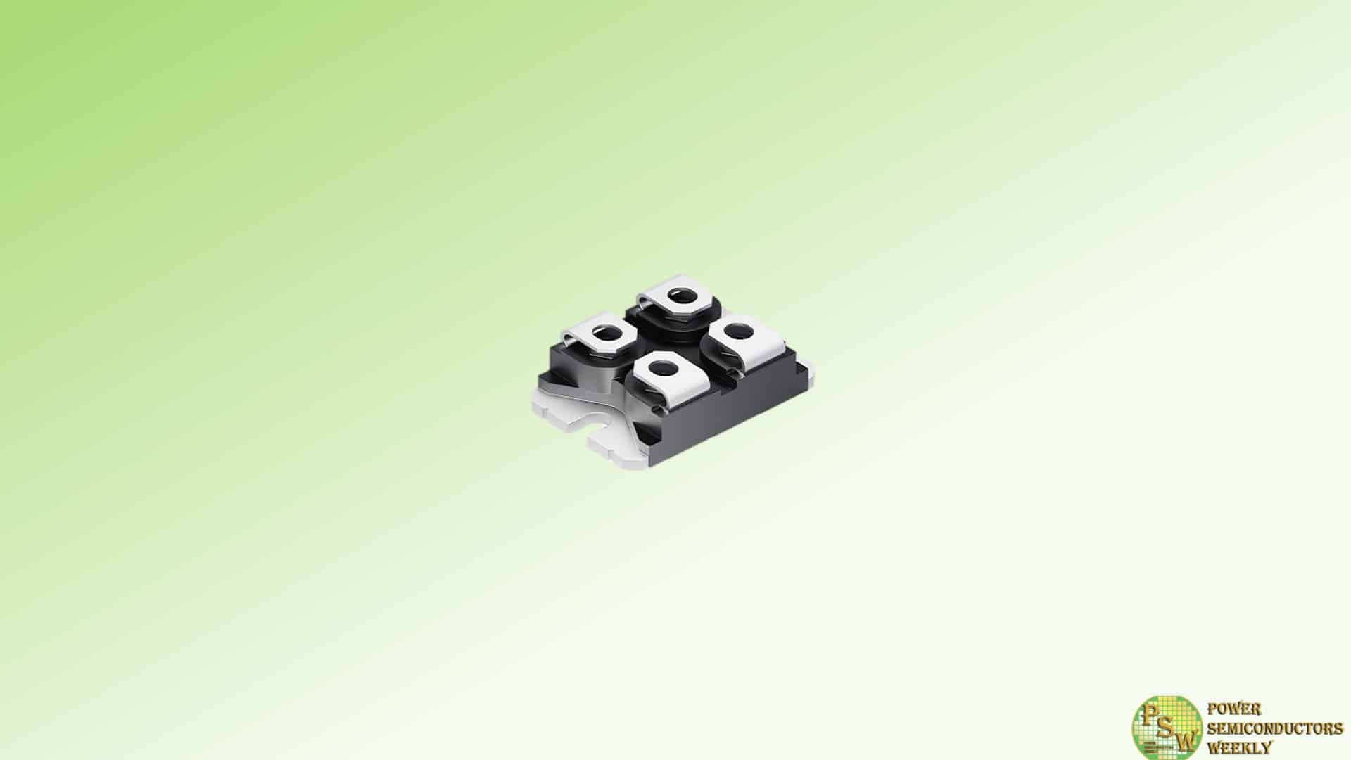
Nexperia announced the launch of 16 new 80 V and 100 V power MOSFETs in the innovative copper-clip CCPAK1212 package, delivering industry-leading power density and outright performance. The innovative copper-clip design provides high current conduction, reduced parasitic inductance, and excellent thermal performance. These features make the devices ideal for motor control, power supplies, renewable energy systems, and other power-hungry applications.
The range also includes application-specific MOSFETs (ASFETs) designed for AI server hot-swap functions. With top-side and bottom-side cooling options, these MOSFETs in CCPAK provide high power density and reliable solutions. All devices are supported by JEDEC registration and Nexperia’s interactive datasheets for seamless integration.
The benchmark PSMN1R0-100ASF is a 0.99 mΩ 100 V power MOSFET capable of conducting 460 A and dissipating 1.55 KW of power, yet in a CCPAK1212 package footprint that occupies only 12mm x 12mm of board space. The PSMN1R0-100CSF offers similar statistics in a top-side cooled version.
The secret to this impressive performance is the internal construction of the devices. The “CC” in CCPAK1212 stands for copper clip, meaning that the power MOSFET silicon die is sandwiched between two pieces of copper, the drain tab on one side and the source clip on the other. With wire bonds entirely eliminated, such an optimized assembly offers a low on-resistance, reduced parasitic inductances, high maximum current ratings and excellent thermal performance.
CCPAK1212 NextPower 80/100 V MOSFETs are recommended for power-hungry industrial applications where high efficiency and high reliability are critical, including brushless DC (BLDC) motor control, switched-mode power supplies (SMPS), battery management systems (BMS) and renewable energy storage. The availability of such power-capable MOSFETs in a single package reduces the need for parallelism, simplifying designs and offering more compact, cost-effective solutions.
The Nexperia CCPAK1212 announcement also includes some new application specific MOSFETs (ASFETs) targeting the hot-swap function in increasingly powerful AI servers. These devices feature an enhanced safe operating area (SOA), providing superior thermal stability during linear mode transitions.
Across all these applications, the availability of top-side and bottom-side cooling options provides engineers a choice of thermal extraction techniques, especially helpful where dissipating heat through the PCB is impractical due to the sensitivity of other components.
“Despite offering market-leading performance, we know that some customers will be reticent to design-in a relatively new package”, stated Chris Boyce, Product Group General Manager at Nexperia. “For this reason, we have registered the CCPAK1212 with the JEDEC standards organization (reference MO-359). We followed a similar approach when we introduced the first LFPAK MOSFET package some years ago and as a result there are now many compatible devices available in the market. You are never on your own for long when your innovations offer genuine value to your customers”, concluded Boyce.
All the new CCPAK1212 MOSFET devices are supported with a range of advanced design-in tools, including thermally compensated simulation models. Traditional PDF datasheets are supplemented with Nexperia’s user-friendly interactive datasheets, which now incorporate a new “graph-to-csv” feature that allows engineers to download, analyze and interpret the data behind each device’s key characteristics. This not only streamlines the design process but enhances confidence in design choices.
Nexperia plans to extend CCPAK1212 packaging to power MOSFETs across all voltage ranges and also to its automotive qualified AEC-Q101 portfolios, addressing the evolving demands of next-generation systems with the highest current and thermal performance requirements.
Original – Nexperia
-

To provide higher efficiency and power density for telecom, industrial, and computing applications, Vishay Intertechnology, Inc. introduced a new 150 V TrenchFET® Gen V n-channel power MOSFET in the PowerPAK® SO-8S (QFN 6×5) package.
Compared to previous-generation devices in the PowerPAK SO-8, the Vishay Siliconix SiRS5700DP slashes overall on-resistance by 68.3% and on-resistance times gate charge — a key figure of merit (FOM) for MOSFETs used in power conversion applications — by 15.4% while providing 62.5% lower RthJC and 179 % higher continuous drain current.
With the industry’s lowest on-resistance of 5.6 mΩ at 10 V and on-resistance times gate charge FOM of 336 mΩ*nC, the device released today minimizes power losses from conduction. This allows designers to boost efficiency to meet next-generation power supply requirements, such as 6 kW AI server power systems. In addition, the extremely low 0.45 °C/W RthJC of the PowerPAK SO-8S package enables continuous drain current up to 144 A to increase power density while providing robust SOA capability.
The SiRS5700DP is ideal for synchronous rectification, DC/DC converters, hot swap switching, and OR-ing functionality. Typical applications will include servers, edge computing, super computers, and data storage; telecom power supplies; solar inverters; motor drives and power tools; and battery management systems. RoHS-compliant and halogen-free, the MOSFET is 100 % Rg and UIS tested and complies with IPC-9701 criteria for more reliable temperature cycling. The device’s standard 6 mm by 5 mm footprint is fully compatible with the PowerPAK SO-8 package.
Original – Vishay Intertechnology
-
Littelfuse, Inc. announced the release of the IXTN400N20X4 and IXTN500N20X4 Ultra Junction X4-Class Power MOSFETs.
The new devices expand upon the current 200 V X4-Class Ultra Junction MOSFETs, featuring some of the lowest on-state resistances available. The high current ratings of these MOSFETs allow designers to replace multiple low-current rated devices connected in parallel, streamlining the design process and enhancing both reliability and power density in applications. Additionally, the screw-mounted terminals of the SOT-227B package enable rugged and stable mounting.
These new 200 V MOSFETs deliver the lowest on-state resistances, enhancing and complementing the existing Littelfuse X4-Class Ultra Junction family portfolio. Compared to the existing state-of-the-art X4-Class MOSFET solutions, these MOSFETs offer up to ~2x higher current ratings and RDS(on) values up to ~63% lower.
The new MOSFETs are ideal for a range of low-voltage power applications where minimizing on-state losses is essential, including:
- Battery Energy Storage Systems (BESS),
- Battery chargers,
- Battery formation,
- DC/battery load switch, and
- Power supplies.
“The new devices will allow designers to replace multiple low-current rated devices, connected in parallel, with a single device solution,” said Sachin Shridhar Paradkar, Global Product Marketing Engineer at Littelfuse. “This unique solution simplifies gate driver design, improves reliability, improves power density and PCB space utilization.”
The Ultra Junction X4-Class Power MOSFET offers the following key performance benefits:
- Low conduction losses
- Minimized parallel connection effort
- Simplified driver design with minimal driver losses
- Simplified thermal design
- Increased power density
A MOSFET with low on-state resistance (RDS(on)) is the ideal choice in applications where minimal on-state losses are crucial. It significantly reduces the power dissipation during operation, leading to lower conduction losses, higher efficiency, and less heat generation. This makes it perfect for power-sensitive applications such as power supplies, motor drivers, and battery-operated devices where maintaining high efficiency and thermal management is crucial.
Performance Specifications
Performance Specs IXTN500N20X4 IXTN400N20X4 Package Aluminum-nitride ceramic-based isolated SOT-227B On-state resistance RDS(on) = 1.99 mΩ @ Tvj = 25°C RDS(on) = 3 mΩ @ Tvj = 25°C High nominal current rating 500 A @ TC = 25°C 340 A @ TC = 25°C Gate charge Qg = 535 nC Qg = 348 nC Thermal resistance RthJC = 0.13 K/W RthJC = 0.18 K/W Original – Littelfuse
-

Power components are evolving to meet the increasing demands for higher efficiency, smaller size and greater performance in power electronic systems. To provide system designers with a wide range of power solutions, Microchip Technology announced its portfolio of IGBT 7 devices offered in different packages, multiple topologies, and current and voltage ranges.
Featuring increased power capability, lower power losses and compact device sizes, this new portfolio is designed to meet high-growth market segments such as sustainability, E-Mobility and data centers. These high-performance IGBT 7 devices are key building blocks for power applications in solar inverters, hydrogen ecosystems, commercial and agricultural vehicles and More Electric Aircraft (MEA).
Designers can select a suitable power solution based on their requirements. The IGBT 7 devices are offered in standard D3 and D4 62 mm packages, as well as SP6C, SP1F and SP6LI packages. Many configurations are available in the following topologies: three-level Neutral-Point Clamped (NPC), three-phase bridge, boost chopper, buck chopper, dual-common source, full-bridge, phase leg, single switch and T-type. Devices are available with voltages ranging from 1200V to 1700V and current ranging from 50A to 900A.
“The versatile IGBT 7 portfolio combines ease of use and cost efficiency with higher power density and reliability, offering our customers maximum flexibility. These products are designed for general industrial applications as well as specialized aerospace and defense applications,” said Leon Gross, corporate vice president of Microchip’s discrete product group. “Additionally, our power solutions can be integrated with Microchip’s broad range of FPGAs, microcontrollers (MCUs), microprocessors (MPUs), dsPiC® Digital Signal Controllers (DSCs) and analog devices to provide a comprehensive system solution from one supplier.”
The lower on-state IGBT voltage (Vce), improved antiparallel diode (lower Vf) and increased current capability can enable lower power losses, higher power density and higher system efficiency. The lower-inductance packages, combined with the higher overload capability at Tvj −175°C, make these devices excellent options for creating rugged and high-reliability aviation and defense applications—such as propulsion, actuation and power distribution—at a lower system cost.
For motor control applications where enhanced controllability of dv/dt is important, the IGBT 7 devices are designed to offer freewheeling softness for efficient, smooth and optimized driving of switches. These high-performance devices also aim to improve system reliability, reduce EMI and minimize voltage spikes.
Original – Microchip Technology
-

ROHM has developed automotive-grade AEC-Q101 qualified 4th Generation 1200V IGBTs that combine class-leading low loss characteristics with high short-circuit resistance. This makes the devices ideal for vehicle electric compressors and HV heaters as well as industrial inverters.
The current lineup includes RGA80TRX2HR / RGA80TRX2EHR / RGA80TSX2HR / RGA80TSX2EHR – in two discrete package types (TO-247-4L and TO-247N), along with 11 bare chip variants – SG84xxWN – with plans to further expand the lineup in the future.
The increasing use of higher voltages in automotive systems and industrial equipment has led to a growing demand for power devices capable of handling high voltages in applications such as vehicle electric compressors, HV heaters, and inverters for industrial equipment.
At the same time, there is a strong push for high efficiency power devices to improve energy conservation, simplified cooling mechanisms, and smaller form factors for a decarbonized society. Automotive electrical components must also comply with automotive reliability standards, while power devices for inverter and heater circuits are required to provide current interruption capabilities during short circuits, necessitating high short-circuit tolerance.
In response, ROHM redesigned the device structure and adopted an appropriate package to develop new 4th Generation IGBTs suitable for high voltage by delivering industry-low loss characteristics with superior short-circuit tolerance.
These devices achieve an industry-leading short-circuit withstand time of 10µs (Tj=25°C) together with low switching and conduction losses while maintaining a high withstand voltage of 1200V and meeting automotive standards by reviewing the device structure, including the peripheral design. At the same time, the new TO-247-4L package products, which feature 4 terminals, can accommodate an effective voltage of 1100V in a ‘Pollution Degree 2 environment’ by ensuring adequate creepage distance between pins. This enables support for higher voltage applications than conventional products.
Implementing creepage distance measures on the device side alleviates the design burden for manufacturers. On top, the TO-247-4L package achieves high-speed switching by including a Kelvin emitter terminal, resulting in even lower losses. In fact, when comparing the efficiency of the new TO-247-4L packages with conventional and standard products in a 3-phase inverter, loss is reduced by about 24% compared to standard products and by 35% over conventional products – contributing to higher efficiency in drive applications.
ROHM will continue to expand its lineup of high-performance IGBTs that contribute to greater miniaturization and high efficiency drive in automotive and industrial equipment applications.
Original – ROHM
-

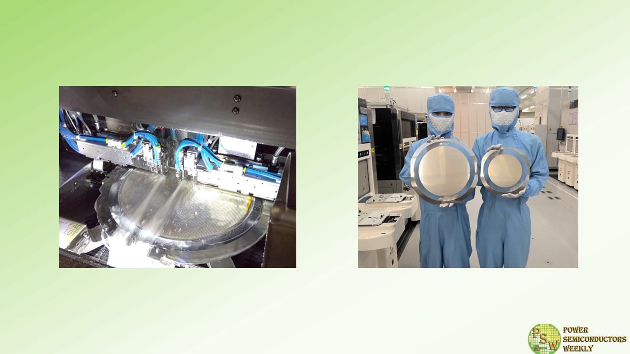
After announcing the world’s first 300-millimeter gallium nitride (GaN) power wafer and opening the world’s largest 200-millimeter silicon carbide (SiC) power fab in Kulim, Malaysia, Infineon Technologies AG has unveiled the next milestone in semiconductor manufacturing technology.
Infineon has reached a breakthrough in handling and processing the thinnest silicon power wafers ever manufactured, with a thickness of only 20 micrometers and a diameter of 300 millimeters, in a high-scale semiconductor fab. The ultra-thin silicon wafers are only a quarter as thick as a human hair and half as thick as current state-of-the-art wafers of 40-60 micrometers.
“The world’s thinnest silicon wafer is proof of our dedication to deliver outstanding customer value by pushing the technical boundaries of power semiconductor technology,” said Jochen Hanebeck, CEO at Infineon Technologies. “Infineon’s breakthrough in ultra-thin wafer technology marks a significant step forward in energy-efficient power solutions and helps us leverage the full potential of the global trends decarbonization and digitalization. With this technological masterpiece, we are solidifying our position as the industry’s innovation leader by mastering all three relevant semiconductor materials: Si, SiC and GaN.”
This innovation will significantly help increase energy efficiency, power density and reliability in power conversion solutions for applications in AI data centers as well as consumer, motor control and computing applications. Halving the thickness of a wafer reduces the wafer’s substrate resistance by 50 percent, reducing power loss by more than 15 percent in power systems, compared to solutions based on conventional silicon wafers.
For high-end AI server applications, where growing energy demand is driven by higher current levels, this is particularly important in power conversion: Here voltages have to be reduced from 230 V to a processor voltage below 1.8 V. The ultra-thin wafer technology boosts the vertical power delivery design, which is based on vertical Trench MOSFET technology and allows a very close connection to the AI chip processor, thus reducing power loss and enhancing overall efficiency.
“The new ultra-thin wafer technology drives our ambition to power different AI server configurations from grid to core in the most energy efficient way,” said Adam White, Division President Power & Sensor Systems at Infineon. “As energy demand for AI data centers is rising significantly, energy efficiency gains more and more importance. For Infineon, this is a fast-growing business opportunity. With mid-double-digit growth rates, we expect our AI business to reach one billion euros within the next two years.”
To overcome the technical hurdles in reducing wafer thickness to the order of 20 micrometers, Infineon engineers had to establish an innovative and unique wafer grinding approach, since the metal stack that holds the chip on the wafer is thicker than 20 micrometers. This significantly influences handling and processing the backside of the thin wafer.
Additionally, technical and production-related challenges like wafer bow and wafer separation have a major impact on the backend assembly processes ensuring the stability and first-class robustness of the wafers. The 20-micrometer thin wafer process builds on Infineon’s existing manufacturing expertise and ensures that the new technology can be seamlessly integrated into existing high-volume Si production lines without incurring additional manufacturing complexity, thus guaranteeing the highest possible yield and supply security.
The technology has been qualified and applied in Infineon’s Integrated Smart Power Stages (DC-DC converter) which have already been delivered to first customers. It underlines the company’s innovation leadership in semiconductor manufacturing as the holder of a strong patent portfolio related to the 20-micrometer wafer technology.
With the current ramp up of the ultra-thin wafer technology Infineon expects a replacement of the existing conventional wafer technology for low voltage power converters within the next three to four years. This breakthrough is bolstering Infineon’s unique position in the market with the broadest product and technology portfolio including silicon, silicon carbide and gallium nitride-based devices which are key enablers of decarbonization and digitalization.
Infineon will present the first ultra-thin silicon wafer publicly at electronica 2024 from 12 to 15 November in Munich (Hall C3, Stand 502).
Original – Infineon Technologies
-

MCC Semi announced the latest innovation in their MOSFET lineup. The 100V wide SOA MCTL2D0N10YHR with split-gate trench technology satisfies the design demands of high-performance applications with ease. Balancing efficiency and reliability in harsh conditions is no longer an issue, thanks to this N-channel power MOSFET’s wide safe operating area (SOA) and a host of efficient characteristics.
This SOA comparison highlights significant differences in drain current between two 100V MOSFETs, MCTL300N10YB and MCTL2D0N10YHR, at 10ms pulse. This MOSFET’s wide SOA enhances safety and performance while overcoming common challenges engineers face when designing for high-power applications. It also provides a host of features that add up to ultimate efficiency and reliability. With a gate charge and on-resistance of 2mΩ, this MOSFET also optimizes energy use at every angle, reducing operational costs.
Designed to withstand junction temperatures of up to 175⁰C, this component delivers unquestionable performance in environments where lesser components would fail. Excellent thermal management is also assured, thanks to the TOLL package engineered for superior heat dissipation, which mitigates thermal-related issues. MCC’s 100V MOSFET is the ideal solution for diverse applications, including telecommunications, computing, audio amplification, and motor controls.
Features & Benefits:
- Wide SOA: Ensures safe operation across a broad range of conditions.
- Split-gate Trench (SGT) Technology: Provides enhanced performance and efficiency.
- Low On-Resistance: Maximizes efficiency by minimizing power losses.
- Low Conduction Losses: Reduces heat generation during operation.
- Low Gate Charge: Maximizes efficiency by minimizing switching losses.
- Low Gate Charge: Maximizes efficiency by minimizing switching losses.
- Excellent Thermal Performance: TOLL package facilitates superior heat dissipation.
Original – Micro Commercial Components
-

Toshiba Electronic Devices & Storage Corporation has expanded the lineup of 150V N-channel power MOSFETs with new six products that use the new generation process “U-MOSⅩ-H series.” Products in this series are suitable for the switching power supplies of industrial equipment such as data centers and communication base. The package of new products is a three-pin through hole type: TO-220 for “TK4R9E15Q5, TK7R2E15Q5 and TK9R6E15Q5” and TO-220SIS for “TK5R0A15Q5, TK7R4A15Q5 and TK9R7A15Q5.”
The new products use the U-MOSⅩ-H process to achieve low drain-source On-resistance. In particular, TK4R9E15Q5 features the excellent low drain-source On-resistance of 4.9mΩ (max). In addition, the new products uses high-speed diode (HSD) to improve reverse recovery characteristics, which are important for synchronous rectification applications, by reducing reverse recovery charge and faster reverse recovery time. Used in synchronous rectification applications, the new products reduce the power loss of switching power supplies and help improve efficiency.
The first product TPH9R00CQ5 which uses HSD, has approximately 74% less reverse recovery charge and approximately 44% faster reverse recovery time than Toshiba‘s existing product TPH9R00CQH, which does not use HSD. The U-MOSⅩ-H process using this HSD has applied to through hole type packages in addition to surface mount type packages.
The new products have reduced the drain source spike voltage generated between the drain and source when MOSFET is switching, helping to lower EMI in switching power supplies.
Toshiba will continue to promote the expansion of its power MOSFET lineup, which helps improve the efficiency of power supplies, thereby contributing to reducing the power consumption of equipment.
Applications
- Switching power supplies for communication equipment, etc. (high efficiency AC-DC converters, high efficiency DC-DC converters, etc.)
- Motor control equipment (motor drives, etc.)
Features
- Excellent low On-resistance:
TK4R9E15Q5 RDS(ON)=4.9mΩ (max) (VGS=10V) - Low reverse recovery charge:
TK9R6E15Q5 Qrr=32nC (typ.) (-dIDR/dt=100A/μs) - Fast reverse recovery time:
TK9R6E15Q5 trr=40ns (typ.) (-dIDR/dt=100A/μs)
Original – Toshiba
-

Affordability combined with high performance and efficiency is the key to making electric mobility accessible to a broader market. That’s why Infineon Technologies AG is introducing the HybridPACK™ Drive G2 Fusion, establishing a new power module standard for traction inverters in the e-mobility sector.
The HybridPACK Drive G2 Fusion is the first plug’n’play power module that implements a combination of Infineon’s silicon and silicon carbide (SiC) technologies. This cutting-edge solution provides an ideal balance between performance and cost efficiency, giving more choice in the optimization of inverters.
One of the main differences between silicon and SiC in power modules is that SiC has a higher thermal conductivity, breakdown voltage and switching speed, making it more efficient, but also more expensive than silicon-based power modules. With the new module, the SiC content per vehicle can be reduced, while maintaining vehicle performance and efficiency at a lower system cost. For example, system suppliers can realize nearly the system efficiency of a full SiC solution with only 30 percent SiC and 70 percent silicon area.
“Our new HybridPACK Drive G2 Fusion module underlines Infineon’s innovation leadership in the automotive semiconductor industry,” said Negar Soufi-Amlashi, Senior Vice President & General Manager High Voltage at Infineon’s Automotive division. “Addressing the demand for greater e-mobility range, this technological breakthrough smartly combines silicon carbide and silicon. Integrated in a well-introduced module package footprint it offers compelling cost-performance ratio over pure silicon carbide modules without adding system complexity for automotive system suppliers and vehicle manufacturers.”
HybridPACK Drive G2 Fusion expands Infineon’s HybridPACK Drive power module portfolio and can be quickly and easily integrated in vehicle components or modules without requiring complex adjustments or configurations. The HybridPACK Drive G2 Fusion module features up to 220 kW in the 750 V class. It ensures high reliability over the entire temperature range from -40 °C to +175 °C and improved thermal conductivity.
The unique properties of Infineon’s CoolSiC™ technology and its silicon IGBT EDT3 technology with very fast turn-on enable the use of a single gate driver or dual gate drivers. This allows easy re-design from full silicon or full SiC based inverters to a fusion inverter. Generally, Infineon’s holistic expertise in SiC MOSFET and silicon IGBT technology, power module packaging, gate drivers as well as sensors enables premium products with cost savings at system level. One example is the integration of Swoboda or XENSIV™ Hall sensors in the HybridPACK Drive package for more precise and efficient motor control.
Infineon will showcase the new HybridPACK Drive G2 Fusion at electronica 2024 in Munich from November 12 to 15 (hall C3, booth 502).
Original – Infineon Technologies
-
Mitsubishi Electric Corporation announced that its Power Device Works’ Fukuyama Factory has begun large-scale supply of power semiconductor chips made from 12-inch silicon (Si) wafers for the assembly of semiconductor modules.
The advanced Si power-semiconductor modules will initially be used in consumer products. Going forward, Mitsubishi Electric expects to contribute to green transformation (GX) by providing a stable and timely supply of semiconductor chips to meet the growing demand for energy-saving power-electronics devices in various applications.
The Fukuyama Factory processes wafers for the production of Si power-semiconductors. The factory is playing a key role in Mitsubishi Electric’s medium-term plan to double its wafer processing capacity for Si power- semiconductors by fiscal 2026 compared to five years earlier. By supplying large quantities of 12-inch Si wafers for power semiconductor chips, the company will ensure stable production of advanced Si power-semiconductor modules for energy-saving power-electronics equipment.
Original – Mitsubishi Electric
