-
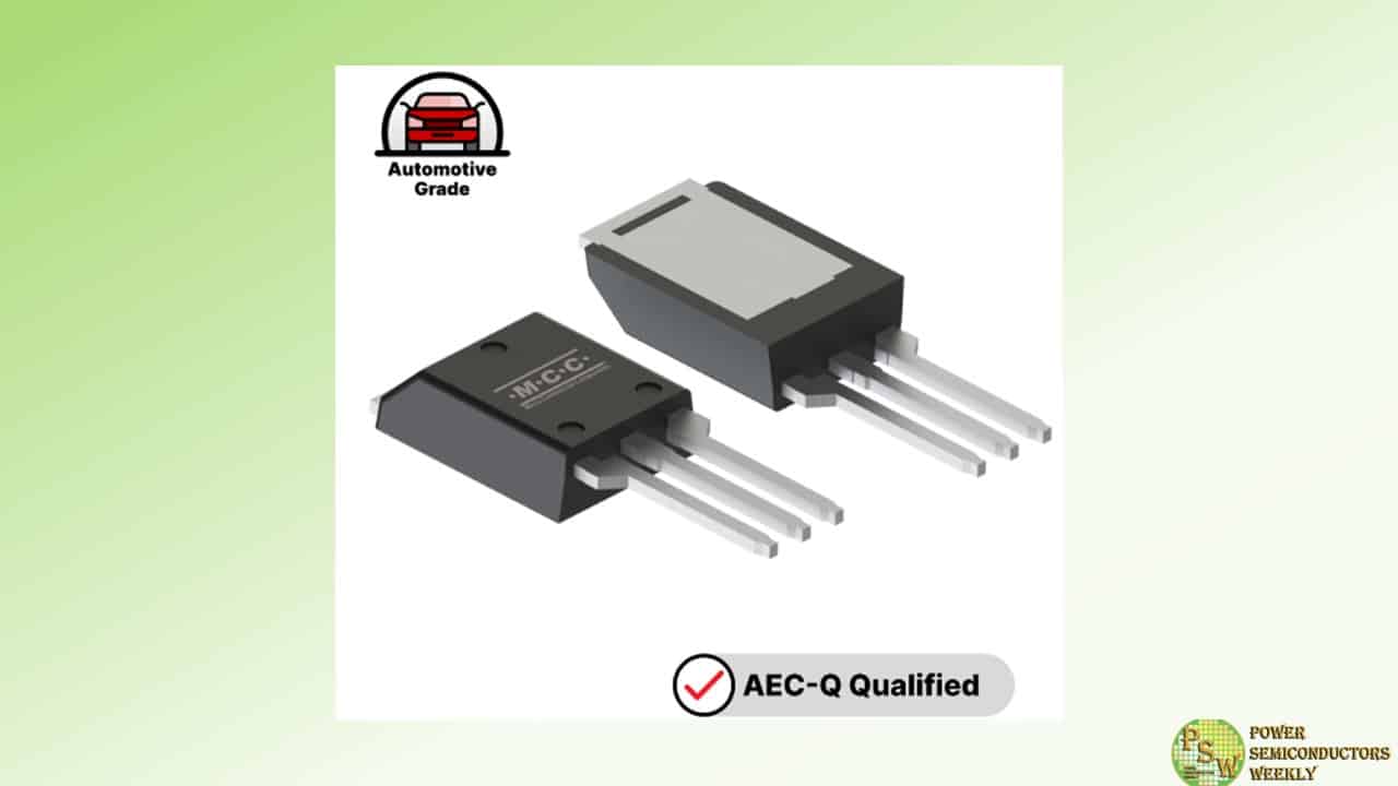
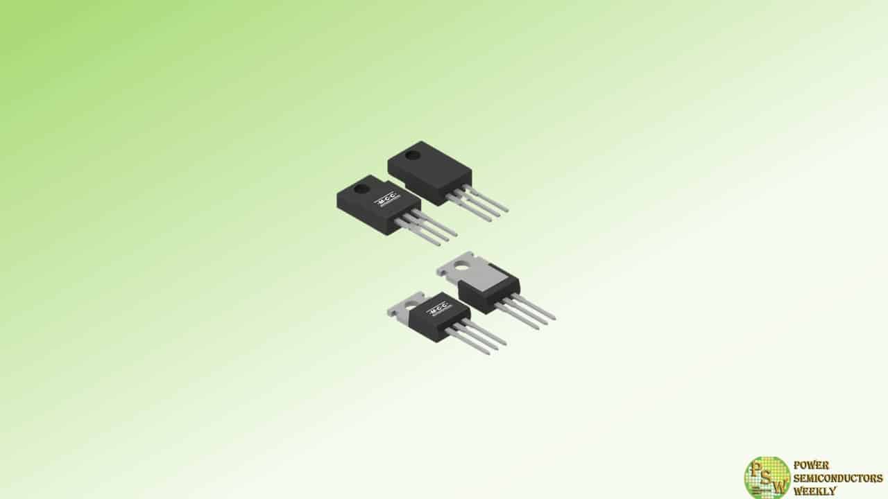
MCC released 1200V Auto-Grade Trench Field-Stop IGBT engineered for demanding automotive applications. MIS80N120NT1YHE3 delivers reliable switching where other components fall short, minimizing losses while maintaining thermal performance.
Its super TO-220 package design boasts a junction-to-case thermal resistance of only 0.17K/W for maximum heat dissipation in high-voltage scenarios. But the superior thermal performance doesn’t stop there. With a low saturated VCE of just 2.25V and operating junction temperature of up to 150°C, this IGBT enhances energy efficiency and boosts overall performance.
Advanced trench field-stop technology provides an additional layer of optimized switching efficiency, adding to its reliability. Rigorously tested to achieve AEC-Q101 qualification, this IGBT is equipped with the robustness required in extreme automotive environments.
From PTC heaters and solid-state relays and electric drive systems, MCC’s new 1200V IGBT is the obvious solution for engineers looking to improve system integrity and efficiency in diverse applications.
Features & Benefits:
- AEC-Q101 Qualified: Meets stringent automotive quality standards for enhanced reliability.
- 1200V High Breakdown Voltage: Capable of handling high-voltage operations, making it ideal for automotive applications.
- Low Saturated VCE: Achieves 2.25V (typ.) at higher temperatures, minimizing energy loss and enhancing efficiency.
- Low Switching Losses: Enable efficient operation, contributing to improved overall system performance.
- Excellent Thermal Performance: Housed in a super TO-220 package (TO-273AA) with a junction-to-case thermal resistance of 0.17K/W, ensuring effective heat dissipation.
- High Thermal Stability: Maintains performance across a wide temperature range for unwavering operation in varying scenarios.
- Powerful Short-Circuit Protection: Integrated features safeguard against damage in fault conditions, enhancing safety and dependability.
- Versatile Application Compatibility: Suitable for a wide range of automotive applications, including PTC heaters, solid-state relays, electric drive systems, renewable energy systems, and industrial motor drives.
Original – Micro Commercial Components
-

JEDEC Solid State Technology Association announced the publication of JEP200: Test Methods for Switching Energy Loss Associated with Output Capacitance Hysteresis in Semiconductor Power Devices. Developed jointly by JEDEC’s JC-70.1 Gallium Nitride and JC-70.2 Silicon Carbide Subcommittees, JEP200 is available for free download from the JEDEC website.
Proliferation of soft switching power conversion topologies brought about the need to accurately quantify the energy stored in a power device’s output capacitance because the energy impacts efficiency of power converters. JEP200, developed in collaboration with academia, addresses the critical power supply industry need to properly test and measure the switching energy loss due to the output capacitance hysteresis in semiconductor power devices and details tests circuits, measurement methods, and data extraction algorithms. The document applies not only to wide bandgap power semiconductors such as GaN and SiC, but also silicon power transistors and diodes.
“Professionals in high-frequency power conversion systems have long sought a standardized approach to testing new switching energy losses,” said Dr. Jaume Roig, Member of Technical Staff, onsemi and Vice Chair of the JC-70 Committee. “This document now provides helpful guidance on testing energy losses related to output capacitance hysteresis caused by displacement currents. With this clarity, system optimization can proceed more accurately.”
“JEDEC’s JC-70 committee has the expertise necessary to meet the demands of the entire power semiconductor industry, and the development of JEP200 demonstrates how the JEDEC process enabled the committee to swiftly respond to an industry need,” said John Kelly, JEDEC President. “JEP200 encompasses GaN, SiC, and Si power devices, helping the industry navigate design challenges caused by the growing number of new power conversion topologies.”
Original – JEDEC
-
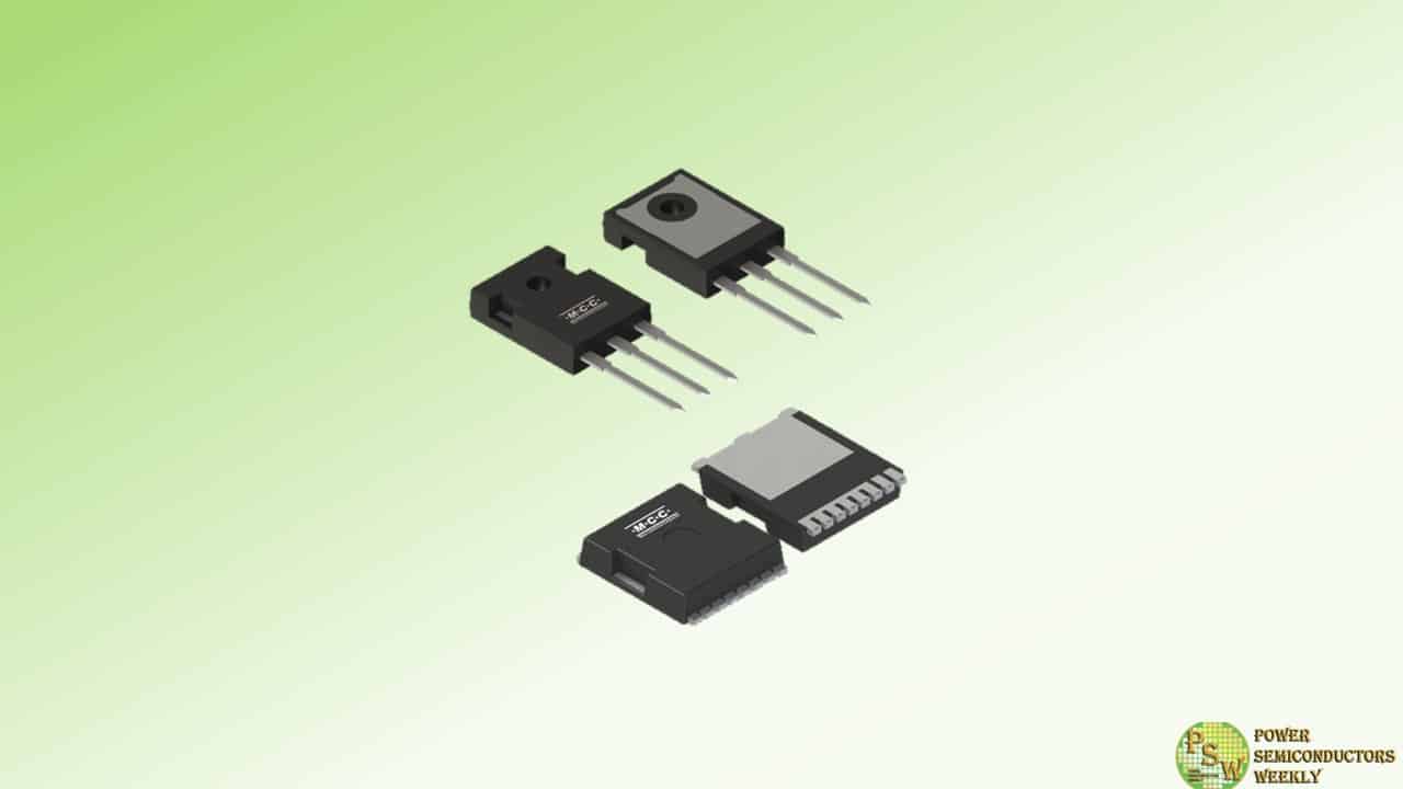
MCC Semi rolled out three new 600V MOSFETs that go beyond high performance. Designed with an integrated fast recovery diode, these advanced components help solve the challenges engineers face when trying to maximize efficiency while minimizing power losses and heat generation.
Ideal for high-voltage applications, MSJWFR60N60, MCTK075N60FH, and MCTK105N60FH feature on-resistance in the sub-100mΩ range — with options as low as 30mΩ — to significantly reduce conduction losses and ensure efficient power delivery.
A low gate charge only adds to their excellence, especially in high-frequency applications where response times are critical. Available in a through-hole TO-247 package and space-saving SMD TOLL-8L options with a Kelvin source connection, these MOSFETs offer a versatile solution for enhancing overall system performance.
Improve reliability for various applications, such as power supplies, AC-DC converters, motor drives, and renewable energy systems, with these low RDS(on) semiconductors from MCC.
Features & Benefits:
- Superjunction MOSFET technology: Enhances efficiency and reduces power losses
- Low on-resistance: Minimizes conduction losses for improved performance
- Low conduction losses: Ensures greater efficiency in power applications
- Low gate charge: Facilitates faster switching and reduced energy consumption
- Integrated fast recovery diode: Provides rapid recovery for better switching performance
- High-speed switching: Supports high-frequency operations, perfect for modern applications
- Versatile packages: Enables design flexibility with through-hole (TO-247) and SMD with Kelvin Source (TOLL-8L-KS) options
Original – Micro Commercial Components
-

onsemi released the newest generation silicon and silicon carbide hybrid Power Integrated Modules (PIMs) in an F5BP package, ideally suited to boost the power output of utility-scale solar string inverters or energy storage system (ESS) applications. Compared to previous generations, the modules offer increased power density and higher efficiencies within the same footprint to increase the total system power of a solar inverter from 300kW up to 350kW.
This means a one-gigawatt (GW) capacity utility-scale solar farm using the latest generation modules can achieve an energy savings of nearly two megawatts (MW) per hour or the equivalent of powering more than 700 homes per year. Additionally, fewer modules are required to achieve the same power threshold as the previous generation, which can reduce power device component costs by more than 25%.
With solar power having achieved the lowest levelized cost of energy (LCOE), it is increasingly becoming the go-to source for renewable power generation around the world. To compensate for solar power’s variability, utility operators are also adding large-scale battery energy storage systems (BESS) to ensure a stable energy flow to the grid. To support this combination of systems, manufacturers and utilities require solutions that offer maximum efficiency and reliable power conversion. Every 0.1% of efficiency improvement can equate to a quarter of a million dollars in annual operational savings for every one gigawatt of installed capacity.
“As a variable energy source dependent on sunlight, continual advances in increasing system efficiencies, reliability and advanced storage solutions are needed to be able to maintain the stability and reliability of global grids during peak and off-peak power demand,” said Sravan Vanaparthy, vice president, Industrial Power Division, Power Solutions Group, onsemi. “A more efficient infrastructure increases adoption and assures us that, as more solar power generation is built out, less energy is wasted and pushes us forward on a path away from fossil fuels.”
The F5BP-PIMs are integrated with 1050V FS7 IGBT and the 1200V D3 EliteSiC diode to form a foundation that facilitates high voltage and high current power conversion while reducing power dissipation and increasing reliability. The FS7 IGBTs offer low turn-off losses and reduce switching losses by up to 8%, while the EliteSiC diodes provide superior switching performance and lower voltage flicker by 15% compared to previous generations.
These PIMs employ an innovative I-type Neutral Point Clamp (INPC) for the inverter module and a flying capacitor topology for the boost module. The modules also use an optimized electrical layout and advanced Direct Bonded Copper (DBC) substrates to reduce stray inductance and thermal resistance. In addition, a copper baseplate further decreases thermal resistance to the heat sink by 9.3%, ensuring the module remains cool under high operational loads. This thermal management is crucial in maintaining the efficiency and longevity of the modules, making them highly effective for demanding applications that require reliable and sustained power delivery.
Original – onsemi
-
MCC Semi unveiled a new 950V MOSFET – MCU1K4N95SH. While traditional MOSFETs often include energy losses and slower switching, this new superjunction (SJ) MOSFET features a low gate-to-drain charge, significantly reducing conduction losses and amplifying overall efficiency.
Its superjunction MOSFET technology and on-resistance of only 1.49Ω empower engineers to design for higher voltage ratings without compromising performance. A DPAK (TO-252) package only adds to this MOSFET’s versatility, making it ideal for AC-DC power supplies, LED lighting, charging adapters, solar and energy devices, and other high-voltage applications across multiple industries.
Features & Benefits:
- Superjunction (SJ) MOSFET technology enhances efficiency
- High-voltage rating of 950V is well-suited for demanding applications
- Low gate charge enables faster switching speeds
- High-speed switching capabilities improve overall performance
Original – Micro Commercial Components
-

Alpha and Omega Semiconductor Limited (AOS) announced its new highly robust power MOSFET LFPAK 5×6 package. AOS’s new LFPAK product offering is available in a wide range of voltages: 40V, 60V, and 100V, and it is designed to withstand harsh environments while maintaining MOSFET performance. The new devices are found in a broad range of applications such as industrial, server power, telecommunications, and solar, where high reliability is required.
AOS’s LFPAK packaging enables higher board-level reliability due to key packaging features such as gull wing leads, which offer a ruggedized solution for board-level environmental stresses. The gull-wing leads also enable optical inspection during PCBA manufacturing. Another feature enhancement is the LFPAK’s larger copper clip, which improves electrical and thermal performance. Advantages of the large clip include improved current handling capabilities, reduced on-resistance, and better heat dispersion compared to wire bonding. A large clip also has low parasitic inductance, enabling lower spike voltage in switching applications. All these features significantly improve the robustness of the MOSFET, and utilizing AOS’s advanced shielded gate MOSFET Technology (AlphaSGT™) enables designers to find an optimized solution to achieve high reliability under the harshest environmental conditions.
“Designers have long trusted AOS power semiconductors in their applications, and LFPAK 5×6 will expand
solution capability,” said Peter H. Wilson, Marketing Sr. Director of the MOSFET product line at AOS.Original – Alpha and Omega Semiconductor
-
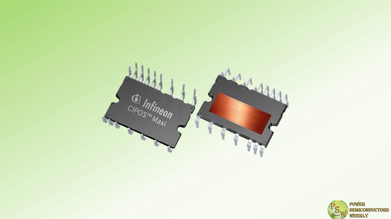
Infineon Technologies AG expands its 7th generation TRENCHSTOP™ IGBT7 product family with the CIPOS™ Maxi Intelligent Power Module (IPM) series for low-power motor drives. The new IM12BxxxC1 series is based on the new TRENCHSTOP IGBT7 1200 V and rapid diode EmCon 7 technology. Thanks to the latest micro-pattern trench design, it offers exceptional control and performance.
This results in significant loss reduction, increased efficiency, and higher power density. The portfolio includes three new products in variants ranging from 10 A to 20 A for power ratings of up to 4.0 kW: IM12B10CC1, IM12B15CC1 and IM12B20EC1.
The IM12BxxxC1 series is packaged in a DIP 36x23D housing. It integrates various power and control components to increase reliability, optimize PCB size and reduce system costs. This makes it the smallest package for 1200 V IPMs with the highest power density and best performance in its class. The IM12BxxxC1 series is particularly suitable for low-power drives in applications such as motors, pumps, fans, heat pumps and outdoor fans for heating, ventilation, and air conditioning.
The new IPM series offers an isolated dual-in-line molded housing for excellent thermal performance and electrical isolation. It also meets the EMI and overload protection requirements of demanding designs. In addition to the protection features, the IPM is equipped with an independent UL-certified temperature thermistor.
The CIPOS™ Maxi integrates a rugged 6-channel SOI gate driver to provide built-in dead time to prevent damage from transients. It features under-voltage lockout at all channels and over-current shutdown. With its multi-function pin, this IPM allows for high design flexibility for various purposes. The low side emitter pins can be accessed for all phase current monitoring making the device easy to control.
Original – Infineon Technologies
-
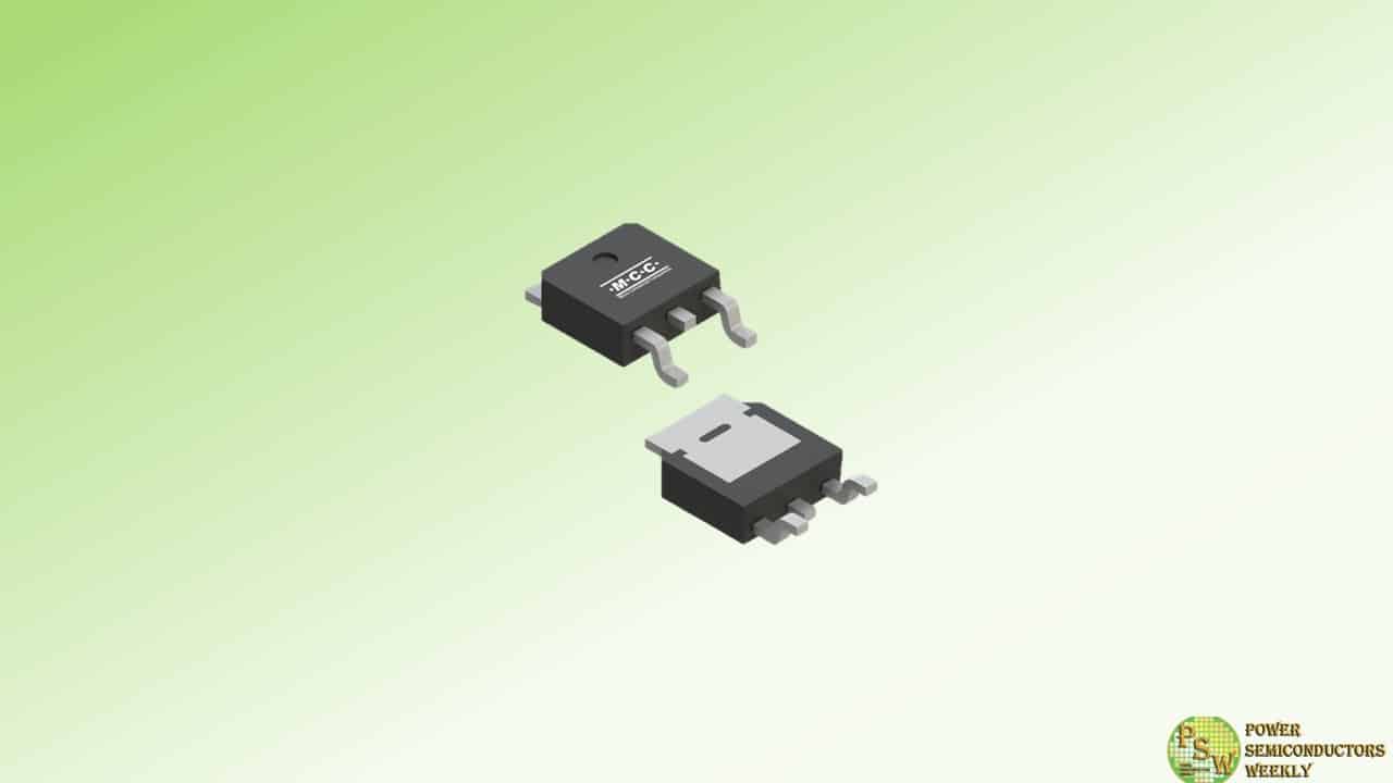
MCC Semi introduced two 600V N-channel MOSFETs with superjunction (SJ) technology. Engineered for maximum efficiency, MSJPFR20N60 and MSJPFFR20N60 boast a low on-resistance of 193mΩ, ensuring minimal power losses. Their integrated fast recovery diode ensures rapid recovery times, dramatically optimizing overall switching performance and circuit reliability.
Superjunction MOSFET technology empowers these components to handle high currents while reducing thermal management needs due to minimal heat dissipation, enhancing efficient operation. Available in isolated (TO-220F) and non-isolated (TO-220AB) packages, these MOSFETs are an excellent and seamless upgrade for existing designs, as well as new products.
For meeting the demands of modern electronics design in high-voltage switching applications, including power supplies, AC-DC converters, and motor drives, our new 600V SJ MOSFETs are the obvious solution.
Features & Benefits:
- Advanced superjunction (SJ) MOSFET technology reduces thermal management requirements
- Low on-resistance of 193mΩ enhances efficiency
- Low conduction losses due to minimal heat dissipation
- Low gate charge improves switching speed and efficiency
- Integrated fast recovery diode empowers high-speed switching
- Seamless integration with non-isolated TO-220AB and isolated TO-220F packages
Original – Micro Commercial Components
-

Nexperia announced that the ongoing expansion of its NextPower 80 V and 100 V MOSFET portfolio is continuing apace with the release of several new LFPAK devices in industry-standard 5×6 mm and 8×8 mm footprints. These new NextPower 80/100 V MOSFETs are optimized for low (RDSon) and low Qrr, to deliver high efficiency and low spiking in applications including servers, power supplies, fast chargers and USB-PD as well as for a wide range of telecommunications, motor control and other industrial equipment. Designers can choose from a range of 80 V and 100 V devices, with (RDSon) from 1.8 mΩ to 15 mΩ.
Many MOSFET manufacturers focus on achieving high efficiency through low QG(tot) and low QGD, when benchmarking the switching performance of their devices against alternative offerings. However, through extensive research, Nexperia has identified Qrr as being even just as important due to its impact on spiking and, in turn, the amount of electromagnetic interference (EMI) generated during device switching.
By focusing on this parameter, Nexperia has considerably reduced the level of spiking produced by its NextPower 80/100 V MOSFETs and hence also lowered the amount of EMI they produce. This brings significant benefits for end users by reducing the probability of a costly late-stage redesign to include additional external components if their application fails electromagnetic compatibility (EMC) testing.
The on-resistance (RDSon) of these new MOSFETs has been reduced by up to 31% compared to currently available devices. Nexperia also plans to further strengthen its NextPower 80/100 V portfolio later this year with the release of an additional LFPAK88 MOSFET offering RDS(on) down to 1.2 mΩ @ 80 V, as well as introducing the power dense CCPAK1212 to the portfolio. To further support design-in and qualification of these devices, Nexperia offers the availability of award-winning interactive datasheets, providing engineers with comprehensive and user-friendly insights into device behavior.
Original – Nexperia
-

Toshiba Electronic Devices & Storage Corporation has expanded its lineup of 600V N-channel power MOSFETs “DTMOSVI series” fabricated with Toshiba’s latest-generation process, with a super junction structure. These new products are suitable for high efficiency switching power supplies used for data centers and power conditioners of photovoltaic generators. Nine products of “TK40N60Z1, TK080N60Z1, TK080A60Z1, TK085V60Z1, TK125N60Z1, TK125A60Z1, TK130V60Z1, TK155A60Z1 and TK165V60Z1” have been added to the lineup in terms of packages and drain-source On-resistance.
By optimizing the gate design and process, 600V DTMOSVI series products have reduced the value of drain-source On-resistance per unit area by approximately 13%, and drain-source On-resistance × gate-drain charge ―the figure of merit for MOSFET performance― by approximately 52% compared to Toshiba’s current generation DTMOSIV-H series products with the same drain-source voltage rating. This means new products have a better trade-off between conduction loss and switching loss than current products. New products of DTMOSVI series will contribute improving efficiency of power supplies.
Toshiba offers tools that support circuit design for switching power supplies. Alongside the G0 SPICE model, which verifies circuit function in a short time, highly accurate G2 SPICE models that accurately reproduce transient characteristics are now available.
Toshiba will continue to expand its DTMOSVI series lineup, and support energy conservation by reducing power loss in switching power supplies.
Original – Toshiba
