-

Leapers Semiconductor has officially commenced construction of its automotive-grade third-generation power semiconductor module project in Jiangdu District’s development zone. The launch event was part of Jiangdu District’s Major Project Construction Mobilization Conference, where local officials outlined key economic initiatives for the region. District Party Secretary Zhu Lili delivered a speech at the ceremony, emphasizing the urgency of driving economic growth from the start of the year. District Mayor Shen Bohong presided over the event, with key government representatives also in attendance.
During the event, township leaders provided updates on the district’s 2025 major construction projects, reaffirming their commitment to economic development. The first quarter alone saw the initiation of 29 major projects, with a total investment of 8.72 billion yuan ($1.2 billion), spanning sectors such as new materials, renewable energy, high-end equipment, and environmental protection.
Leapers Semiconductor SiC module project, which began construction on March 1, represents a 10 billion yuan ($1.4 billion) investment, covering an area of 32 acres. Once completed, the facility is expected to achieve an annual production capacity of 3 million automotive-grade SiC modules, generate 10 billion yuan ($1.4 billion) in annual revenue, and contribute 500 million yuan ($70 million) in annual tax revenue.
With this new SiC module packaging and testing facility, Leapers Semiconductor is set to enhance production capabilities, accelerate innovation, and drive the adoption of SiC power solutions worldwide.
Original – Leapers Semiconductor
-
 LATEST NEWS / PRODUCT & TECHNOLOGY / PROJECTS / SiC / TOP STORIES / WBG
February 27, 2025
4 Min ReadSilicon carbide (SiC) provides considerable technical advantages for power electronics – however, the costs are still a drawback. In the »ThinSiCPower« research project, a consortium of Fraunhofer Institutes is developing key technologies to reduce material losses and device thickness while increasing the thermomechanical stability of the assembled SiC chips. The savings achieved are expected to help further accelerate the market development of efficient SiC power electronics.
Power electronics based on the wide-bandgap semiconductor silicon carbide (SiC) are a key enabler for energy-efficient, sustainable and high-performance applications in electromobility – from cars and commercial vehicles to trains, ships and airplanes, in the generation, transportation and storage of renewable energies, as well as for IT and industrial infrastructures. It is therefore an important and competitively relevant factor for the current global transformation processes in the areas of mobility, energy and digitalization. The market for SiC power devices is expected to grow at an annual rate of over 30 percent. Compared to conventional silicon technology, the use of SiC power electronics in a standard drive converter saves more energy than is required to manufacture the SiC power electronics themselves.
While the technological advantages of SiC are obvious due to its physical properties, the higher costs compared to the established silicon are still an obstacle to faster market penetration. Chip costs are more than three times higher than for silicon. The initially required SiC wafer is the biggest cost driver here. In the case of a SiC-based metal-oxide semiconductor field-effect transistor (MOSFET), this accounts for more than 40 percent of the manufacturing costs. In addition, due to the unfavorable mechanical material properties and large thickness of the monocrystalline SiC wafer, electronics processed from it only achieve approx. 30 percent of the thermomechanical service life compared to silicon. This disadvantage leads to an approx. 25 percent larger chip area and, in the case of an inverter for example, to around 25 percent higher costs in the application.
In the three-year ThinSiCPower project (2024-2027), funded by the Fraunhofer PREPARE program, researchers are developing an alternative way to produce cost-effective SiC substrates and significantly thinner SiC chips using more resource-efficient processing technologies. Rather than first sawing the expensive, high-quality SiC wafers with the usual material loss and later back-grinding them in device processing, the SiC crystal is separated directly into thinner wafers using a special laser process without any major loss of material, which are then bonded onto an inexpensive carrier substrate based on polycrystalline SiC.
Fraunhofer ISE, ENAS and IWM with the Fraunhofer IISB as project coordinator are pooling their individual competencies in ThinSiCPower. A SiC coating technology developed by Fraunhofer IISB is being adapted for the manufacturing of the poly-SiC carrier substrates, which is more cost- and resource-efficient than the conventional manufacturing method using chemical vapor deposition. The low-loss separation of the thin SiC wafers is carried out using a laser for defined mechanical pre-damage (Fraunhofer ISE) and subsequent separation under well-defined mechanical conditions for controlled crack propagation (Fraunhofer IWM).
The wafer bonding process for the poly-SiC substrate with the split SiC, including the necessary surface preparation before and after the bonding process, will be developed at Fraunhofer ENAS, while the subsequent device processing and qualification will take place at Fraunhofer IISB. The partners are also developing adapted electrical test methods at thin wafer level as well as physics-of-failure simulation models to maximize the market acceptance of this new class of low-cost SiC substrates. With this, a broad applicability in the relevant industries could be achieved.
The aim is to reduce SiC device costs by 25 percent by developing technology for the production of costeffective thin SiC wafers and poly-SiC substrates. In addition, SiC design costs are to be reduced by further 25 percent by increasing the load cycle stability by 300 percent. The target markets are semiconductor and power module manufacturers as well as their process and equipment suppliers through to test equipment suppliers. With this project, the participating partner institutes are also combining their expertise to set up a complete, highly innovative and future-oriented SiC processing line within the Research Fab Microelectronics Germany (FMD). The consortium is receiving consultancy support directly from partners in industry.
The ThinSiCPower project not only accelerates the market penetration of silicon carbide through the targeted cost reduction and conceptual advantages, but also serves to secure an innovative, resilient and industry relevant SiC technology value chain in Germany and Europe.
Original – Fraunhofer IISB
-

SemiQ Inc will give the first official unveiling of the company’s new 1700 V and 1200 V Gen 3 SiC MOSFETs at the 2025 Applied Power Electronics Conference (APEC).
APEC takes place at the Georgia World Congress Center in Atlanta from March 16, with SemiQ’s booth located at stand #1348.
SemiQ’s 1200 V Gen3 SiC was announced in February, delivering an improved performance with a smaller die size and at a lower cost. The series includes automotive qualified (AEC-Q101) options and Known Good Die (KGD) testing has been implemented across the series with verification at voltages exceeding 1400 V, plus avalanche testing to 800 mJ. Reliability is further improved through 100% gate-oxide burn-in screening and UIL testing of discrete packaged devices.
The company’s new 1700 V MOSFET family of MOSFETS and modules with AEC-Q101 certification is designed to meet the needs of medium-voltage high power conversion applications, from photovoltaic, wind inverters and energy storage to EV and roadside charging as well as uninterruptable power supplies, and induction heating/welding. These switching planar D-MOSFETs enable more compact system designs with higher power densities and have been tested to KGD beyond 1900 V, with UIL avalanche testing to 600 mJ.
Dr. Timothy Han, President at SemiQ said: “There is so much innovation happening in power electronics right now and we’re delighted to have launched our next generation technologies in time to have them on display at APEC. The show brings together many of the leading minds within the industry and we’re looking forward to discussing the challenges faced and how we can help them.”
Original – SemiQ
-
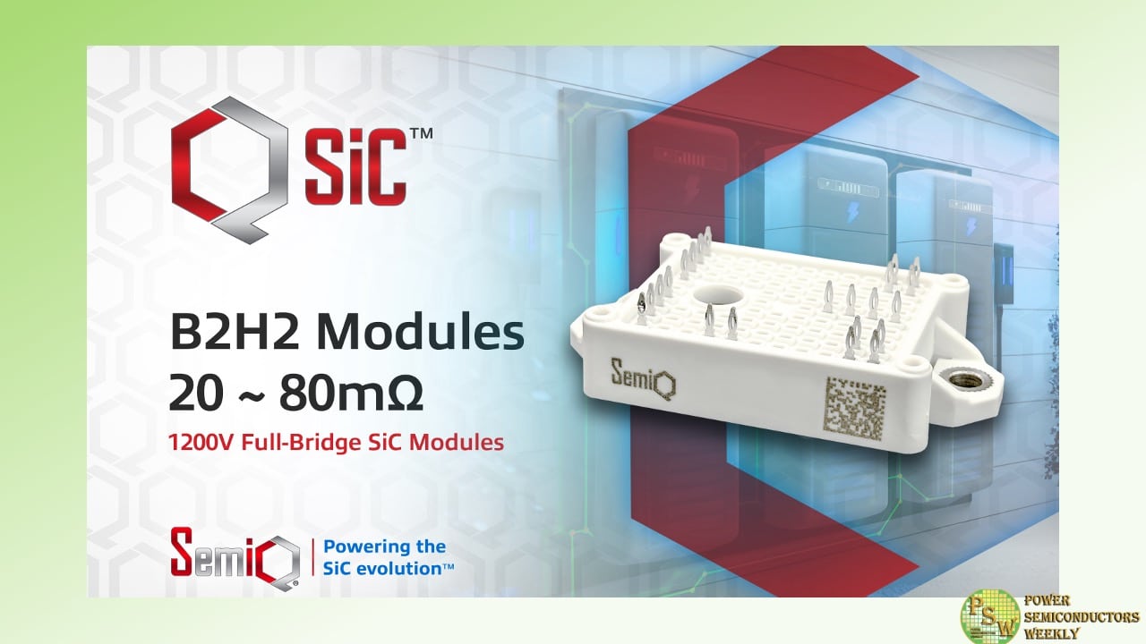
SemiQ Inc has announced a family of three 1200V SiC full-bridge modules, each integrating two of the company’s rugged high-speed switching SiC MOSFETs with reliable body diode. The modules have been developed to simplify the development of photovoltaic inverters, energy storage, battery charging and other high-frequency DC applications.
Available in 18, 38 and 77mΩ (RDSon) variants, the modules have been tested at voltages exceeding 1350V and deliver a continuous drain current of up to 102A, a pulsed drain current of up to 250A and a power dissipation of up to 333W.
Operational with a junction temperature of up to 175oC, the rugged B2 modules have exceptionally low switching losses (EON 0.13mJ, EOFF 0.04mJ at 25oC – 77mΩ module), low zero-gate voltage drain/gate source leakage (0.1µA/1nA – all modules) and low junction to case thermal resistance (0.4oC per watt – 18mΩ module).
“By integrating high-speed SiC MOSFETs with exceptional performance and reliability, our new QSiC 1200V family of full-bridge modules sets a new standard for power density and efficiency in demanding DC applications. This family of modules simplifies system design, and enables faster time-to-market for next-generation solar, storage, and charging solutions,” said Seok Joo Jang, Director of Module Engineering at SemiQ.
Available immediately, the modules can be mounted directly to a heat sink, are housed in a 62.8 x 33.8 x 15.0mm package (including mounting plates) with press fit terminal connections and split DC negative terminals.
Original – SemiQ
-

Navitas Semiconductor is set to unveil a breakthrough in power conversion that will create a paradigm shift across multiple major end markets. These developments include both semiconductor and system innovations which are expected to drive major improvements in energy efficiency & power density and further accelerate the adoption of gallium nitride and silicon carbide technologies to displace silicon.
The live-streamed event will take place on March 12th at 8 am PST and will be re-streamed (in both Chinese and English) at 6 pm PST.
Co-founders, Gene Sheridan (CEO), Dan Kinzer (CTO, COO) and Jason Zhang (VP Engineering) will uncover this next inflection in power conversion, including technology details, specific application examples and describe the expected market impacts & business opportunities from these innovations.
- Register now, 8 am Pacific: https://bit.ly/NavitasLiveEvent-8am-PT
- Register now, 6 pm Pacific: https://bit.ly/NavitasLiveEvent-6pm-PT
Original – Navitas Semiconductor
-

Infineon Technologies AG has made significant progress on its 200 mm silicon carbide (SiC) roadmap. The company will already release the first products based on the advanced 200 mm SiC technology to customers in Q1 2025. The products, manufactured in Villach, Austria, provide first-class SiC power technology for high-voltage applications, including renewable energies, trains, and electric vehicles. Additionally, the transition of Infineon’s manufacturing site in Kulim, Malaysia, from 150-millimeter wafers to the larger and more efficient 200-millimeter diameter wafers is fully on track. The newly built Module 3 is poised to commence high-volume production aligned with market demand.
“The implementation of our SiC production is progressing as planned and we are proud of the first product releases to customers,” said Dr. Rutger Wijburg, Chief Operations Officer of Infineon. “By ramping up SiC production in Villach and Kulim in phases, we are improving cost-efficiency and continuing to ensure product quality. At the same time, we are making sure our manufacturing capacities can meet the demand for SiC-based power semiconductors.”
SiC semiconductors have revolutionized high-power applications by switching electricity even more efficiently, demonstrating high reliability and robustness under extreme conditions, and by making even smaller designs possible. Infineon’s SiC products let customers develop energy-efficient solutions for electric vehicles, fast charging stations and trains as well as renewable energy systems and AI data centers.
The release to customers of the first SiC products based on the 200-millimeter wafer technology marks a substantial step forward in Infineon’s SiC roadmap, with a strong focus on providing customers with a comprehensive portfolio of high-performance power semiconductors that promote green energy and contribute to CO 2 reduction.
As “Infineon One Virtual Fab” for highly innovative wide-bandgap (WBG) technologies, Infineon’s production sites in Villach and Kulim share technologies and processes which allow for fast ramping and smooth and highly efficient operations in SiC and gallium nitride (GaN) manufacturing. The 200-millimeter SiC manufacturing activities now add to Infineon’s strong track record of delivering industry-leading semiconductor technology and power system solutions and strengthen the company’s technology leadership across the entire spectrum of power semiconductors, in silicon as well as in SiC and GaN.
Original – Infineon Technologies
-

The electronics industry is experiencing a significant shift towards more compact and powerful systems. To support this trend and further drive innovation at the system level, Infineon Technologies AG is expanding its portfolio of discrete CoolSiC™ MOSFETs 650 V with two new product families housed in Q-DPAK and TOLL packages.
These diverse product families, with top- and bottom-side cooling, are based on the CoolSiC™ Generation 2 (G2) technology and offer significantly improved performance, reliability, and ease of use. The product families target high- and medium-power switched-mode power supplies (SMPS) including AI servers, renewable energy, chargers for electric vehicles, e-mobility and humanoid robots, televisions, drives and solid-state circuit breakers.
The TOLL package offers outstanding Thermal Cycling on Board (TCoB) capability, enabling compact system designs by reducing the printed circuit board (PCB) footprint. When used in SMPS, it can also reduce system-level manufacturing costs. The TOLL package now fits an extended list of target applications, enabling PCB designers to further reduce costs and better meet market demands.
The introduction of the Q-DPAK package complements the ongoing development of Infineon’s new family of Topside Cooled (TSC) products, which includes CoolMOS™ 8, CoolSiC™, CoolGaN™ and OptiMOS™. The TSC family enables customers to achieve excellent robustness with maximum power density and system efficiency at low cost. It also enables direct heat dissipation of 95 percent, allowing the use of both sides of the PCB for better space management and reduction of parasitic effects.
The CoolSiC™ MOSFETs 650 V G2 in TOLL are now available in R DS(on) from 10 to 60 mΩ, while the Q-DPAK variant is available in 7, 10, 15 and 20 mΩ.
Original – Infineon Technologies
-
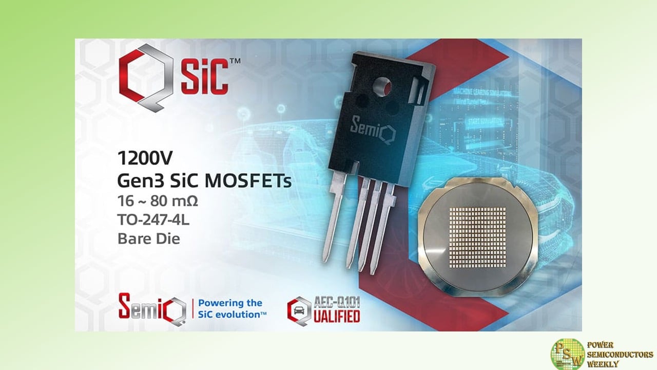
SemiQ Inc has announced the QSiC 1200V MOSFET, a third-generation SiC device that shrinks the die size while improving switching speeds and efficiency.
The device is 20% smaller versus QSiC’s second-generation SiC MOSFETs and has been developed to increase performance and cut switching losses in high-voltage applications. SemiQ is targeting a diverse range of markets including EV‑charging stations, solar inverters, industrial power supplies and induction heating.
It will be on display for the first time at the Applied Power Electronics Conference (APEC), on March 16-20, 2025.
In addition to having a drain-to-source voltage (VDS) of 1200 V, the MOSFET reduces total switching losses to 1646 µJ and has a low on-resistance (RDS,on) of 16.1 mΩ. It is available as a bare die or in a four-pin TO-247 4L discrete package measuring 31.4 x 16.1 x 4.8 mm, which includes a reliable body diode and a driver-source pin for gate driving.
High-quality Known Good Die (KGD) testing has been conducted using UV tape and Tape & Reels, with all parts undergoing testing and verification at voltages exceeding 1400V, as well as being avalanche tested to 800 mJ. Reliability is further improved through the device’s 100% wafer-level gate oxide burn-in screening and 100% UIL testing of discrete packaged devices.
The device has been developed to have a low reverse recovery charge (QRR 470 nC) and lower capacitance, improving switching speed, switching losses, EMI and overall efficiency; to be easy to parallel; and with a longer creepage distance (9 mm), improving electrical insulation, voltage tolerance and reliability.
Dr. Timothy Han, President at SemiQ said: “The move to Gen3 SiC further increases the benefits of SiC MOSFETs over IGBTs. These devices not only deliver vastly improved performance, but cut die size and cost versus previous generations. As a result, the launch of the QSiC 1200V opens the technology, and its benefits, to a far greater range of applications. The device delivers industry leading performance figures, notably on gate threshold voltage, and we’re delighted to be demonstrating this first at APEC.”
The QSiC 1200V MOSFETs has a continuous operational and storage temperature of -55oC to 175oC. It has a recommended operational gate-source voltage of -4/18 V, with a VGSmax of -8/22 V, and a power dissipation of 484 W (core and junction temperature 25oC).
For static electrical characteristics, the device has a junction-to-case thermal resistance of 0.26oC per watt (40oC per watt junction to ambient). Its Zero gate voltage drain current is 100 nA, with a gate-source voltage current of 10 nA. Its AC characteristics include a turn-on delay time of 21 ns with rise time of 25 ns; its turn-off delay time is 65 ns with a fall time of 20 ns.
An increased range of resistances is available in bare-die and TO-247 4L packages with the following options:
- 16 mΩ: GP3T016A120X / GP3T016A120H
- 20 mΩ: GP3T020A120X / GP3T020A120H
- 40 mΩ: GP3T040A120X / GP3T040A120H
- 80 mΩ: GP3T080A120X / GP3T040A120H
Both the 16 mΩ (AS3T016A120X / AS3T016A120H) and 40 mΩ (AS3T040A120X / AS3T040A120H) options have been qualified for Automotive Applications Product Validation according to AEC-Q101.
The SemiQ QSiC 1200V will be on display at the Georgia World Congress Center in Atlanta, from March 16 to 20, 2025. Visitors to SemiQ’s booth #1348 will have the opportunity to explore the new third-generation MOSFETs.
Original – SemiQ
-

Navitas Semiconductor’s 8.5kW power supply unit (PSU), powered by GaNFast™ and GeneSiC™ technologies, has been recognized for its innovative design. Tailored for AI and hyperscale data centers, the PSU achieves 98% efficiency while meeting Open Compute Project (OCP) and Open Rack v3 (ORv3) specifications.
The design minimizes ripple current, EMI, and device count by 25%, reducing costs. Its 3-phase LLC topology utilizes GaNSafe™ technology with integrated control, drive, sensing, and protection, along with Gen-3 Fast SiC MOSFETs for enhanced performance and reliability.
Original – Navitas Semiconductor
-

Navitas Semiconductor announced its adoption of both technologies into Dell’s family of notebook adapters, from 60 W to 360 W.
Enabled by over 20 years of SiC technology leadership, GeneSiC leads on performance of SiC MOSFETs with patented ‘trench-assisted planar’ technology and 5th-gen GeneSiC silicon carbide (SiC) diodes to deliver high-speed, high-efficiency performance with proprietary ’low-knee’ technology for cool operation.
Navitas’ GaNFast power ICs enable high-frequency, high-efficiency power conversion, achieving 3x more power and 3x faster charging in half the size and weight compared to prior designs with legacy silicon power devices.
Navitas GaN & SiC technology together enables Dell to provide high-speed charging, with highest efficiency, coolest temperature, smallest size, and lowest material count. Dell’s latest line-up of AI notebooks includes Neural Processor Units (NPUs), which are dedicated AI engines, to manage sustained AI and AI offload. This builds on Dell’s portfolio as the broadest GaN adapter offering for notebooks in the industry.
The new adapters will also help Dell achieve its advanced sustainability goals, with a focus on CO2 reduction and energy reduction. The adapter cases require up to 50% less plastic and are made with post-recycled materials, significantly reducing energy waste, and improving resource utilization. Navitas’ GaNFast and GeneSiC technologies increase the level of system integration and switching frequency, which reduces the number of components, as well as the size, resulting in a ‘dematerialization’ that lowers carbon footprint throughout the production, packaging, and logistics processes. Each GaNFast power IC shipped saves 4 kg CO2 and every SiC MOSFET shipped saves 25 kg CO2 vs. legacy silicon power chips.
“Since Dell’s first GaN adapter was enabled by Navitas back in 2020, we’ve worked closely with Dell engineering to further improve charging speed, efficiency, size, weight, and now environmental footprint”, said Gene Sheridan, CEO and co-founder of Navitas. “Dell’s new adapters are an optimal solution for speed, portability, and sustainability. Our clients achieve a win-win for both the market and environment by deploying Navitas GaNFast power ICs and GeneSiC power devices.”
Original – Navitas Semiconductor
