-
Toshiba Electronic Devices & Storage Corporation has developed a Schottky barrier diode (SBD) embedded metal oxide semiconductor field effect transistor (MOSFET), a significant improvement over the current device structure, while maintaining high reliability and short-circuit ruggedness.
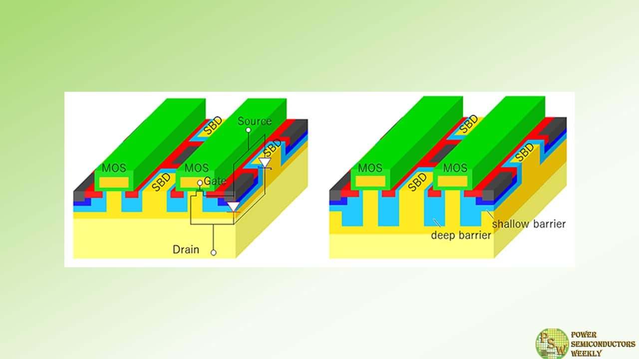
A successful design modification introduces a barrier structure with varying depths in the device structure that maintains the reliability of the reverse conduction operation, the function of an integrated SBD, while suppressing the current leakage from the SBD part that causes destruction during short-circuiting. By making use of new design technology and optimizing the device structure, the new MOSFET achieves lower on-resistance (RonA), with about a 26% improvement over the current structure.
Power semiconductors play a central role in electricity supply and control. They cut energy consumption in all kinds of electronic equipment, and are an important tool for the realization of carbon neutrality. Continued demand expansion is expected from vehicle electrification and the miniaturization of industrial equipment.
Against this background, SiC MOSFETs are seen as next-generation power semiconductors. They deliver better power energy conversion efficiency than Si MOSFETs, and their use has expanded rapidly in recent years. However, SiC MOSFETs have a reliability problem: increased RonA due to reverse conduction operation. Toshiba has now developed an SBD-embedded SiC MOSFET that operates in reverse conduction without increasing RonA.
Reducing the RonA of SiC MOSFET simultaneously causes excess current flow through the MOSFET part during short-circuit operation, reducing the durability of short-circuit operation. However, enhancing the conduction of the embedded SBD to improve the reliability of reverse conduction operation increases its current leakage during short-circuit operation, which also decreases the durability of short-circuit operation.
Introducing a deep barrier structure can suppress both the excess current of the MOSFET and SBD current leakage during short-circuit operation, but it also obstructs current flow from the SBD, raising concerns about decreased reliability in diode conduction.
This led Toshiba to consider a barrier structure divided into shallow and deep areas. The deep barrier area successfully suppresses excess current from the MOSFET part during short-circuit operation, and reduces SBD current leakage, while leaving a shallow area effectively spreads current from the SBD without any obstruction by the barrier.
This improves ruggedness during short-circuit operation while maintaining excellent reliability in reverse conduction operation. Toshiba has provided some customers with test samples of SiC MOSFETs with embedded SBD that apply the new technology since December 2023 for evaluation, toward further enhancing performance.
By making use of its new design technology and optimizing the device structure, Toshiba has developed a prototype 1.2 kV class SBD-integrated MOSFET. This achieves a low RonA of 2.0 mΩcm2, about a 26% improvement over the current structure. Toshiba will present the details of this technology at The 36th International Symposium on Power Semiconductor Devices and ICs (ISPSD) 2024, an international conference on power semiconductors, which is being held in Bremen, Germany from June 2 to 6.
Original – Toshiba
-
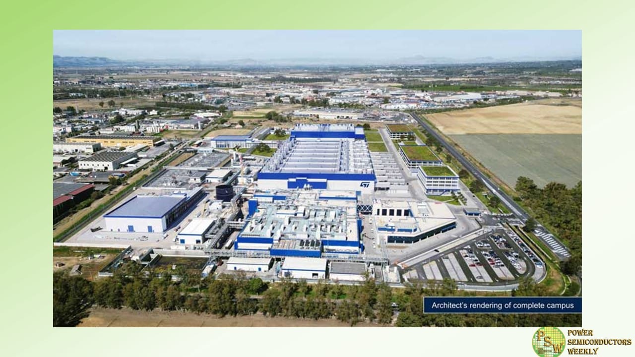
STMicroelectronics announced a new high-volume 200mm silicon carbide (“SiC”) manufacturing facility for power devices and modules, as well as test and packaging, to be built in Catania, Italy. Combined with the SiC substrate manufacturing facility being readied on the same site, these facilities will form ST’s Silicon Carbide Campus, realizing the Company’s vision of a fully vertically integrated manufacturing facility for the mass production of SiC on one site.
The creation of the new Silicon Carbide Campus is a key milestone to support customers for SiC devices across automotive, industrial and cloud infrastructure applications, as they transition to electrification and seek higher efficiency.
“The fully integrated capabilities unlocked by the Silicon Carbide Campus in Catania will contribute significantly to ST’s SiC technology leadership for automotive and industrial customers through the next decades,” said Jean-Marc Chery, President and Chief Executive Officer of STMicroelectronics. “The scale and synergies offered by this project will enable us to better innovate with high-volume manufacturing capacity, to the benefit of our European and global customers as they transition to electrification and seek more energy efficient solutions to meet their decarbonization goals.”
The Silicon Carbide Campus will serve as the center of ST’s global SiC ecosystem, integrating all steps in the production flow, including SiC substrate development, epitaxial growth processes, 200mm front-end wafer fabrication and module back-end assembly, as well as process R&D, product design, advanced R&D labs for dies, power systems and modules, and full packaging capabilities. This will achieve a first of a kind in Europe for the mass production of 200mm SiC wafers with each step of the process – substrate, epitaxy & front-end, and back-end – using 200 mm technologies for enhanced yields and performances.
The new facility is targeted to start production in 2026 and to ramp to full capacity by 2033, with up to 15,000 wafers per week at full build-out. The total investment is expected to be around five billion euros, with a support of around two billion euros provided by the State of Italy within the framework of the EU Chips Act. Sustainable practices are integral to the design, development, and operation of the Silicon Carbide Campus to ensure the responsible consumption of resources including water and power.
Original – STMicroelectronics
-
With the increasing power requirements of Artificial Intelligence (AI) processors, server power supplies (PSUs) must deliver more and more power without exceeding the defined dimensions of the server racks. This is driven by a surge in energy demand of high-level GPUs, which could consume 2 kW and more per chip by the end of the decade.
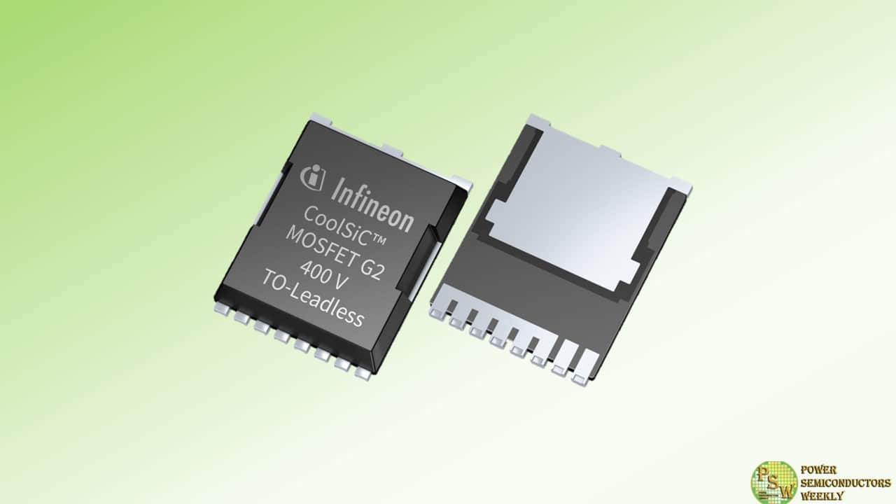
These needs, as well as the emergence of increasingly demanding applications and the associated specific customer requirements have prompted Infineon Technologies AG to extend the development of SiC MOSFETs to voltages below 650 V. The company is now launching the new CoolSiC™ MOSFET 400 V family, which is based on the second generation (G2) CoolSiC technology introduced earlier this year.
The new MOSFET portfolio was specially developed for use in the AC/DC stage of AI servers, complementing Infineon’s recently announced PSU roadmap. The devices are also ideal for solar and energy storage systems (ESS), inverter motor control, industrial and auxiliary power supplies (SMPS) as well as solid-state circuit breakers for residential buildings.
“Infineon offers an extensive portfolio of high-performance MOSFETs and GaN transistors to meet the demanding design and space requirements of AI server power supplies”, said Richard Kuncic, Head of the Power Systems Business Line at Infineon. “We are committed to supporting our customers with advanced products such as the CoolSiC MOSFETs 400 V G2 to drive highest energy efficiency in advanced AI applications.”
The new family features ultra-low conduction and switching losses when compared to existing 650 V SiC and Si MOSFETs. Implemented in a multi-level PFC, the AC/DC stage of the AI Server PSU can attain a power density of more than 100 W/in³ and is proven to reach 99.5 percent efficiency.
This is an efficiency improvement of 0.3 percentage points over solutions using 650 V SiC MOSFETs. In addition, the system solution for AI Server PSUs is completed by implementing CoolGaN™ transistors in the DC/DC stage. With this combination of high-performance MOSFETs and transistors, the power supply can deliver more than 8 kW with an increase in power density by a factor of more than 3 compared to current solutions.
The new MOSFET portfolio comprises a total of 10 products: five R DS(on) classes from 11 to 45 mΩ in Kelvin-source TOLL and D²PAK-7 packages with .XT package interconnect technology. The drain-source breakdown voltage of 400 V at T vj = 25°C. makes them ideal for use in 2- and 3-level converters and for synchronous rectification.
The components offer high robustness under harsh switching conditions and are 100 percent avalanche tested. The highly robust CoolSiC technology in combination with the .XT interconnect technology enables the devices to cope with power peaks and transients caused by sudden changes in the power requirements of the AI processor. Both the connection technology and a low and positive R DS(on) temperature coefficient enable excellent performance under operating conditions with higher junction temperatures.
Original – Infineon Technologies
-
The influence of artificial intelligence (AI) is driving up the energy demand of data centers across the globe. This growing demand underscores the need for efficient and reliable energy supply for servers. Infineon Technologies AG opens a new chapter in the energy supply domain for AI systems and unveils a roadmap of energy efficient power supply units (PSU) specifically designed to address the current and future energy need of AI data centers.
By introducing unprecedented PSU performance classes, Infineon enables cloud data center and AI server operators to reduce their energy consumption for system cooling. The innovative PSUs reduce power consumption and CO 2 emissions, resulting in lower lifetime operating costs. The powerful PSUs are not only used in future data centers but can also replace existing power supply units in servers and increase efficiency.
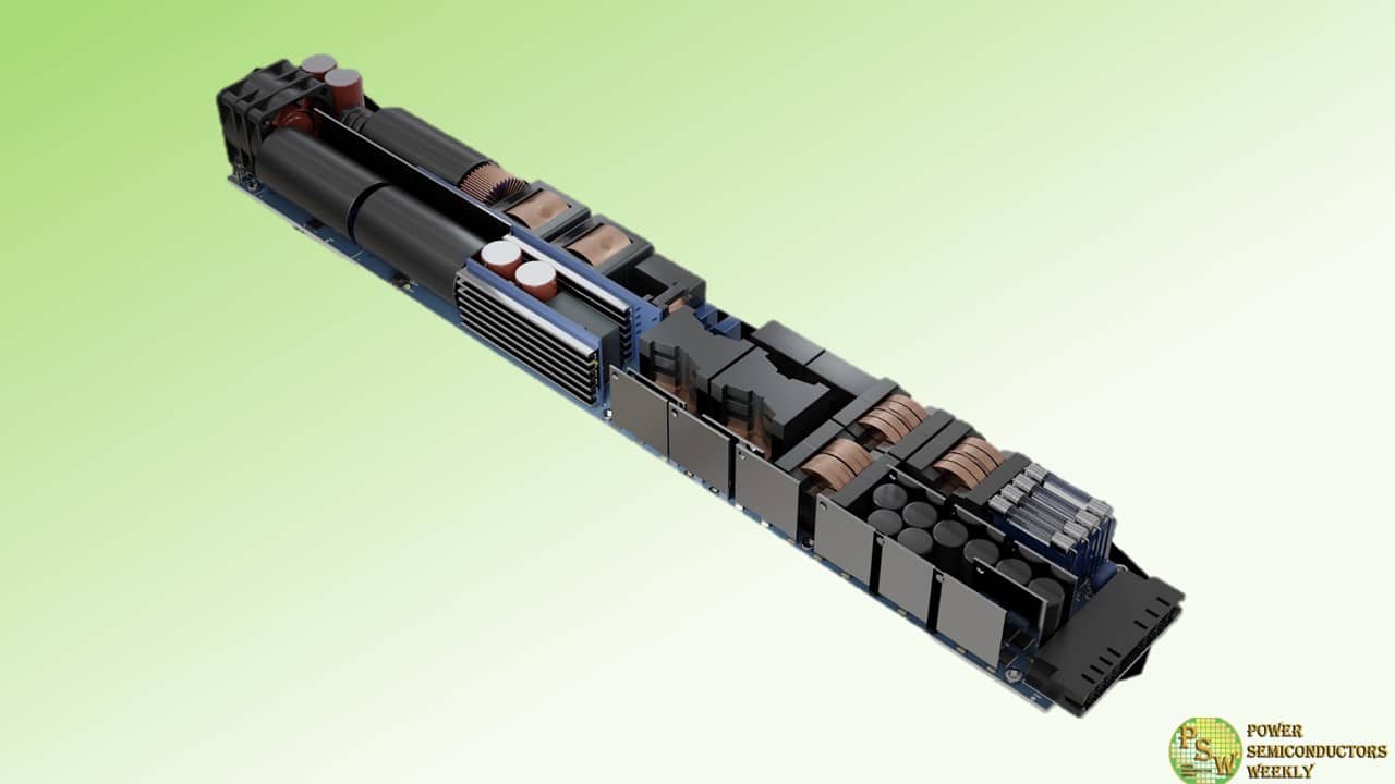
In addition to the current PSUs with an output of 3 kW and 3.3 kW available today, the new 8 kW and 12 kW PSUs will contribute to further increasing energy efficiency in future AI data centers. With the 12 kW reference board, Infineon will offer the world’s first power supply unit that achieves this level of performance and supplies future data centers with power.
“At Infineon, we power AI. We are addressing a critical question of our era – how to efficiently meet the escalating energy demands of data centers,” says Adam White, Division President Power & Sensor Systems at Infineon. “It’s a development that was only possible by Infineon’s expertise in integrating the three semiconductor materials silicon (Si), silicon carbide (SiC), and gallium nitride (GaN) into a single module. Our PSU portfolio is therefore not only an example of Infineon’s innovative strength, which leads to first-class results in terms of performance, efficiency and reliability for data centers and the AI ecosystem. It also reinforces Infineon’s market leadership in power semiconductors.”
Infineon is responding to the requirements of data center operators for higher system efficiency and lower downtimes. The growth of server and data center applications has led to an increase in power requirements, necessitating the development of power supplies with higher power ratings from 800 W up to 5.5 kW and beyond. This increase is driven by the growing power requirements of Graphic Process Units (GPU) on which AI applications are computed.
High-level GPUs now require up to 1 kW per chip reaching 2 kW and beyond by the end of the decade. This will lead to higher overall energy demand for data centers. Depending on the scenario, data centers will account for up to seven percent of global electricity consumption by 2030; this is an order of magnitude comparable to India’s current electricity consumption.
Infineon’s new PSUs contribute to the efforts to limit the CO 2 footprint of AI data centers despite the rapidly growing energy requirements. This is made possible by a particularly high level of efficiency that minimizes power losses. Infineon’s new generation PSUs achieve an efficiency of 97.5 percent and meet the most stringent performance requirements. The new 8 kW PSU is capable of supporting AI racks with an output of up to 300 kW and more. Efficiency and power density is increased to 100 watts per in³ compared to 32 W/in³ in the available 3 kW PSU, providing further benefits for the system size and cost savings for operators.
From a technical perspective, this is made possible by the unique combination of the three semiconductor materials Si, SiC and GaN. These technologies contribute to the sustainability and reliability of AI server and data center systems. Innovative semiconductors based on wide-bandgap materials such as SiC and GaN are the key to a conscious and efficient use of energy to drive decarbonization.
The 8 kW Power Supply Unit will be available in Q1 2025. For more information about the PSU roadmap, please click here.
Infineon at the PCIM Europe 2024
PCIM Europe will take place in Nuremberg, Germany, from 11 to 13 June 2024. Infineon will present its products and solutions for decarbonization and digitalization in hall 7, booths #470 and #169. Company representatives will also be giving several presentations at the accompanying PCIM Conference and Forums, followed by discussions with the speakers. Information about Infineon’s PCIM 2024 show highlights is available at www.infineon.com/pcim.
Original – Infineon Technologies
-

Soitec and Tokai Carbon, a comprehensive manufacturer of carbon and graphite products, have entered into a strategic partnership for the development and supply of polycrystalline silicon carbide substrates specifically designed for Soitec SmartSiC™ wafers.
Silicon carbide is a disruptive compound semiconductor and SmartSiC™ engineered substrates accelerate the adoption of silicon carbide for electric mobility, industrial and smart grid applications by delivering superior manufacturing and cost efficiencies with an improved environmental footprint.
Under this partnership, which will see Tokai Carbon supply 150mm and 200mm poly-SiC wafers to Soitec, the two companies are harnessing their advanced R&D capabilities to enhance the SmartSiC™ ecosystem. Tokai Carbon’s advanced technology and manufacturing capacity in polycrystalline silicon carbide (polySiC) combined with the right to use Soitec specifications for polySiC coarse wafers compliant with Soitec SmartSiC™ is expected to make a strategic contribution to the global ramp-up of SmartSiC™ wafer production.
Cyril Menon, Chief Operations Officer of Soitec, stated: “This partnership with Tokai marks yet another key step in the ramp-up of Soitec’s SmartSiC™ technology to address fast-growing markets such as electric mobility and industrial electrification. Tokai’s top quality SiC products and R&D capabilities, combined with Soitec’s innovative SmartSiC™ technology, can help to accelerate global adoption of electric mobility and other SiC technologies. This is an important milestone in terms of perception and value creation for the SmartSiC™ ecosystem.”
Hajime Nagasaka, CEO of Tokai Carbon, commented. “The polycrystalline SiC substrate to be supplied to Soitec is a strategic product in our solid SiC product series. We are pleased to see our long years of research and development come to fruition in this way, and we have high expectations for this product in the SiC semiconductor market, which is expected to expand significantly in the future. The partnership with Soitec is also very meaningful in terms of contributing to the realization of a sustainable society.”
Original – Soitec
-
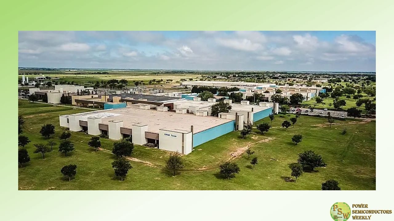
X-FAB and Soitec will begin work to offer Soitec’s SmartSiC™ wafers for the production of silicon carbide power devices at X-FAB’s plant in Lubbock, Texas.
This collaboration follows the successful completion of the assessment phase, during which silicon carbide (SiC) power devices were manufactured at X-FAB Texas on 150mm SmartSiC™ wafers. Soitec will offer X-FAB’s customers easy access to the SmartSiC™ substrate through a joint supply chain consignment model.
X-FAB is the pioneer and leader of the foundry model in the fast-growing SiC market. Silicon carbide (SiC) is a disruptive compound semiconductor material with intrinsic properties providing superior performance and efficiency over silicon in power applications.
SmartSiC™ is a proprietary Soitec technology based on the company’s SmartCut™ process, in which a thin layer of a high-quality monocrystalline (mono-SiC) ‘donor’ wafer is split off and bonded to a low resistivity polycrystalline (poly-SiC) ‘handle’ wafer. The resulting substrate offers improved device performance and manufacturing yields. The process allows multiple re-uses of a single donor wafer, significantly reducing cost and related CO2 emissions.In this fast-growing market, Soitec is ramping production of SmartSiC™ substrates at its new plant of Bernin, near Grenoble (France). X-FAB is increasing production capacity for SiC devices at the Lubbock plant. The use of the SmartSiC™ substrate enables X-FAB’s customers to design smaller devices, resulting in efficiency improvements through an increased number of dies per wafer. The benefit of reduced CO2 emissions from the substrate manufacturing process will also contribute to X-FAB’s initiative to reduce its overall carbon footprint.
Sophie Le-Guyadec VP Procurement of X-FAB, states: “As the leading SiC foundry, we want to provide our customers the full range of opportunities to design innovative and robust SiC devices for electric vehicles, renewable power and industrial applications. To offer the most advanced silicon carbide processes and manufacturing capabilities, we jointly agreed to provide our customers easy access to Soitec’s innovative SmartSiC™ via a consignment model.”
Emmanuel Sabonnadiere, Soitec Executive Vice President Automotive and Industry comments: “Soitec’s SmartSiC substrates and X-FAB’s foundry services are a perfect fit to meet increasing demand for new SiC products. This cooperation is a significant milestone for the deployment of SmartSiC in the U.S. market and internationally, thanks to X-FAB’s global footprint.”Original – X-FAB
-
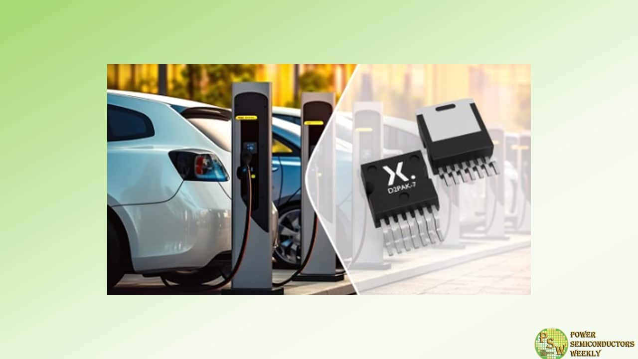
Nexperia announced that it is now offering its industry leading 1200 V silicon carbide (SiC) MOSFETs in D2PAK-7 surface mount device (SMD) packaging, with a choice of 30, 40, 60, and 80 mΩ RDSon values. This announcement follows on from Nexperia’s late-2023 release of two discrete SiC MOSFETs in 3 and 4-pin TO-247 packaging and is the latest offering in a series which will see its SiC MOSFET portfolio swiftly expand to include devices with RDSon values of 17, 30, 40, 60 and 80 mΩ in flexible package options.
With the release of the NSF0xx120D7A0, Nexperia is addressing the growing market demand for high performance SiC switches in SMD packages like D2PAK-7, which is becoming increasingly popular in various industrial applications including electric vehicle (EV) charging (charge pile, offboard charging), uninterruptible power supplies (UPS) and inverters for solar and energy storage systems (ESS).
It is also further testimony to Nexperia’s successful strategic partnership with Mitsubishi Electric Corporation (MELCO), which has seen the two companies join forces to push the energy efficiency and electrical performance of SiC wide bandgap semiconductors to the next level, while additionally future-proofing production capacity for this technology in response to ever growing market demand.
RDSon is a critical performance parameter for SiC MOSFETs because it impacts conduction power losses. However, many manufacturers concentrate on the nominal value, neglecting the fact that it can increase by more than 100% as device operating temperatures rise, resulting in considerable conduction losses.
Nexperia identified this as a limiting factor in the performance of many currently available SiC devices and leveraged the features of its innovative process technology to ensure that its new SiC MOSFETs offer industry-leading temperature stability, with the nominal value of RDSon increasing by only 38% over an operating temperature range from 25 °C to 175 °C.
Tightest threshold voltage, VGS(th) specification, allows these discrete MOSFETs to offer balanced current-carrying performance when connected in parallel. Furthermore, low body diode forward voltage (VSD) is a parameter which increases device robustness and efficiency, while also relaxing the dead-time requirement during freewheeling operation.
Original – Nexperia
-
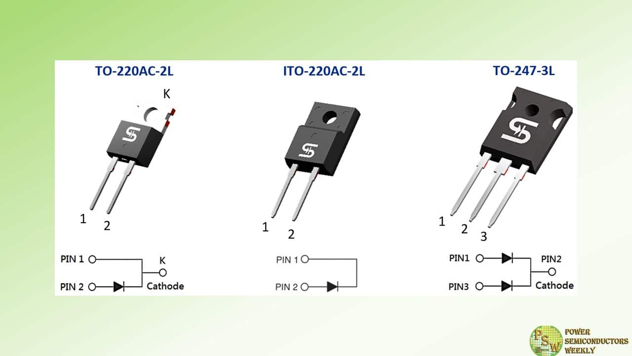
Taiwan Semiconductor – a global supplier of discrete power electronics devices, LED drivers, analog ICs and ESD protection devices – announced a family of 650V silicon carbide Schottky barrier diodes which are suitable for high-efficiency AC-DC, DC-DC and DC-AC conversion applications.
Unlike silicon-based fast-recovery rectifiers, these SiC devices have negligible switching losses due to low capacitive charge (QC). This makes them suitable for high-speed switching applications, benefitting circuit designs with increased power density and can reduce overall solution size.
Key Features
- Max. junction temperature 175°C
- High-speed switching
- High frequency operation
- Positive temperature coefficient on VF
- SPICE Models available
- Thermal Models available
Applications
- AD-DC conversion – PFC Boost
- DC-DC, Solar inverters
- Data center and server power
- Telecom – Datacom power
- UPS systems
Circuit Functions
- PFC boost diode
- Free-wheeling diode
- Full wave bridge
- Vienna bridgeless circuit
Original – Taiwan Semiconductor
-
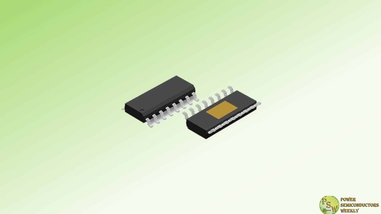
Littelfuse, Inc. announced the launch of the IX4352NE Low-side SiC MOSFET and IGBT Gate Driver. This innovative driver is specifically designed to drive Silicon Carbide (SiC) MOSFETs and high-power Insulated Gate Bipolar Transistors (IGBTs) in industrial applications.
The key differentiator of the IX4352NE lies in its separate 9 A source and sink outputs, which enable tailored turn-on and turn-off timing while minimizing switching losses. An internal negative charge regulator also provides a user-selectable negative gate drive bias for improved dV/dt immunity and faster turn-off. With an operating voltage range (VDD – VSS) of up to 35 V, this driver offers exceptional flexibility and performance.
One of the standout features of the IX4352NE is its internal negative charge pump regulator, which eliminates the need for an external auxiliary power supply or DC/DC converter. This feature is particularly valuable for turning off SiC MOSFETs, saving valuable space typically required for external logic level translator circuitry. The logic input’s compatibility with standard TTL or CMOS logic levels further enhances space-saving capabilities.
The IX4352NE is ideally suited for driving SiC MOSFETs in various industrial applications such as:
- on-board and off-board chargers,
- Power Factor Correction (PFC),
- DC/DC converters,
- motor controllers, and
- industrial power inverters.
It’s superior performance makes it ideal for demanding power electronics applications in the electric vehicle, industrial, alternate energy, smart home, and building automation markets.
With its comprehensive features, the IX4352NE simplifies circuit design and offers a higher level of integration. Built-in protection features such as desaturation detection (DESAT) with soft shutdown sink driver, Under Voltage Lockout (UVLO), and thermal shutdown (TSD) ensure the protection of the power device and the gate driver. The integrated open-drain FAULT output signals a fault condition to the microcontroller, enhancing safety and reliability. Furthermore, the IX4352NE saves valuable PCB space and increases circuit density, contributing to overall system efficiency.
Notable improvements over the existing IX4351NE include:
- A safe DESAT-initiated soft turn-off.
- A thermal shutdown with high threshold accuracy.
- The charge pump’s ability to operate during thermal shutdown.
The new IX4352NE is pin-compatible, allowing for a seamless drop-in replacement in designs that specify the existing Littelfuse IX4351NE, which was released in 2020.
“The IX4352NE extends our broad range of low-side gate drivers with a new 9 A sink/source driver, simplifying the gate drive circuitry needed for SiC MOSFETs,” commented June Zhang, Product Manager, Integrated Circuits Division (SBU) at Littelfuse. “Its various built-in protection features and integrated charge pump provide an adjustable negative gate drive voltage for improved dV/dt immunity and faster turn-off. As a result, it can be used to drive any SiC MOSFET or power IGBT, whether it is a Littelfuse device or any other similar component available on the market.”
Original – Littelfuse
-

Infineon Technologies AG will provide silicon carbide (SiC) power modules HybridPACK™ Drive G2 CoolSiC™ and bare die products to Xiaomi EV for its recently announced SU7 until 2027. Infineon’s CoolSiC-based power modules allow for higher operating temperatures, resulting in best-in-class performance, driving dynamics and lifetime.
Traction inverters based on the technology can, for example, further increase electric vehicle range. The HybridPACK Drive is Infineon’s market-leading power module family for electric vehicles, with almost 8.5 million units sold since 2017.
Infineon provides two HybridPACK Drive G2 CoolSiC 1200 V modules for the Xiaomi SU7 Max. In addition, Infineon supplies Xiaomi EV with a broad range of products per car, including, for example, EiceDRIVER TM gate drivers and more than ten microcontrollers in various applications. The two companies also agreed to further cooperate on SiC automotive applications to fully utilize the benefits of Infineon’s SiC portfolio.
Zhenyu Huang, Vice President of Xiaomi EV and General Manager of the Supply Chain Department, said: “Infineon is an important partner with leading technologies and resilient manufacturing capabilities in power semiconductors as well as a highly scalable microcontroller product portfolio. The cooperation between the two companies will not only help stabilize the supply of silicon carbide for Xiaomi EV, but also help us build a high-performance, safe and reliable luxury car with leading-edge features for our customers.”
Peter Schiefer, President of Infineon’s Automotive division, said: “We are very pleased to work with dynamic players such as Xiaomi EV and provide them with silicon carbide products designed to enhance the performance of electric cars even further. As the leading partner to the automotive industry, we are well positioned with our broad product portfolio, system understanding and multi-site manufacturing base to shape the mobility of the future.”
This collaboration contributes to Infineon’s position as the number one partner of the global automotive industry. According to the latest data from TechInsights, Infineon is the largest semiconductor supplier to the automotive industry. In addition to its number one position in automotive power semiconductors, Infineon also took the lead in the field of automotive microcontrollers last year.
Original – Infineon Technologies
