-

Coherent Corp. announced that it has closed the $1 billion aggregate investment by DENSO CORPORATION and Mitsubishi Electric Corporation in Coherent’s silicon carbide semiconductor business.
Under the terms of the transaction announced on October 10, 2023, DENSO and Mitsubishi Electric each invested $500 million in exchange for a 12.5% non-controlling ownership interest in the Business, with Coherent owning the remaining 75%. Coherent has separated and contributed the Business to a new subsidiary that will operate the Business. Going forward, all operating and capital expenses of the Business will be funded by the Business. Coherent will control and operate the Business, which will continue to be led by Sohail Khan, Executive Vice President, Wide-Bandgap Electronics.
In connection with the transaction, the Business has entered into arm’s-length long-term supply arrangements with DENSO and Mitsubishi Electric that support their demand for 150 mm and 200 mm silicon carbide (SiC) substrates and epitaxial wafers.
“As I mentioned in October, we are excited to expand our strategic relationships with DENSO and Mitsubishi Electric to capitalize on the significant demand for silicon carbide,” said Dr. Vincent D. Mattera, Jr., Chair and CEO, Coherent.
“I believe that such a close relationship with two leaders in SiC power devices and modules is the best path forward to maximize shareholder value and position the Business for long-term growth. The investments from our strategic partners will be used to accelerate our capacity expansion plans and help sustain our leadership position, while ensuring the development of a robust and scalable supply for the rapidly growing market for SiC-based power electronics, largely driven by the explosive growth of the global electric vehicle market.”
“Through this strategic relationship with Coherent, we will secure a stable procurement of SiC wafers, which are critical for battery electric vehicles, and contribute to the realization of a carbon-neutral society by promoting the widespread adoption of BEVs in all regions around the world,” said Shinnosuke Hayashi, President & COO, Representative Member of the Board at DENSO.
Dr. Masayoshi Takemi, Executive Officer, Group President, Semiconductor & Device for Mitsubishi Electric, said, “We are pleased that this investment has been successfully completed. Going forward, we will further strengthen our collaboration with Coherent, leveraging their capabilities in development and manufacturing of SiC substrates, to achieve solid growth of our SiC power device business and contribute to a more sustainable world through decarbonization.”
When incorporated into electric vehicles and industrial infrastructure, SiC-based power electronics have demonstrated the potential to significantly reduce carbon dioxide emissions and accelerate the transition to a cleaner and more energy-efficient world.
Market estimates indicate that the SiC total addressable market will grow from $3 billion in 2022 to $21 billion in 2030, representing a 28% compound annual growth rate.
The transaction builds on Coherent’s more than two decades of demonstrated leadership in SiC materials. In recent years, the Company has aggressively invested to scale its manufacturing of 150 mm and 200 mm substrates to address this underserved market.
Over the past two years, Coherent has invested aggressively in capital and R&D for SiC. The closing of this $1 billion combined investment into the Business will accelerate the Company’s capital plans in the coming years. Specifically, the investment will fund the manufacturing expansion of the Business and, in combination with the concurrent supply agreements, enhance its position in the market.
The transaction enables Coherent to increase its available free cash flow to provide greater financial and operational flexibility to execute its capital allocation priorities, as it expects the aggregate $1 billion investment will be used to fund future capital expenditure requirements of the Business.
Original – Coherent
-
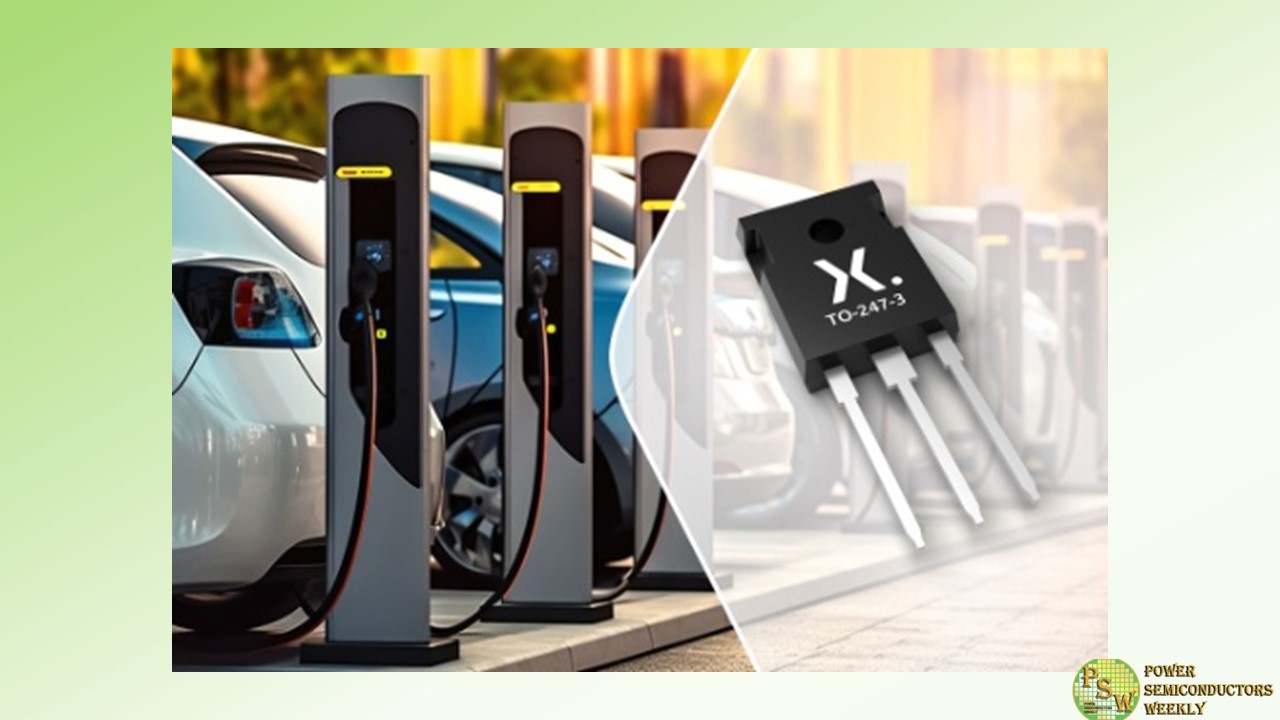
Nexperia announced its first silicon carbide (SiC) MOSFETs with the release of two 1200 V discrete devices in 3-pin TO-247 packaging with RDS(on) values of 40 mΩ and 80 mΩ. NSF040120L3A0 and NSF080120L3A0 are the first in a series of planned releases which will see Nexperia’s SiC MOSFET portfolio quickly expand to include devices with a variety of RDS(on) values in a choice of through-hole and surface mounted packages.
This release addresses the market demand for the increased availability of high performance SiC MOSFETs in industrial applications including electric vehicle (EV) charging piles, uninterruptible power supplies (UPS) and inverters for solar and energy storage systems (ESS).
“With these inaugural products, Nexperia and Mitsubishi Electric wanted to bring true innovation to a market that has been crying out for more wide-bandgap device suppliers”, according to Katrin Feurle, Senior Director & Head of Product Group SiC at Nexperia. “Nexperia can now offer SiC MOSFET devices which offer best-in-class performance across several parameters, including high RDS(on) temperature stability, low body diode voltage drop, tight threshold voltage specification as well as a very well-balanced gate charge ratio making the device safe against parasitic turn on. This is the opening chapter in our commitment to producing the highest quality SiC MOSFETs in our partnership with Mitsubishi Electric. Together we will undoubtedly push the boundaries of SiC device performance over the coming years”.
“Together with Nexperia, we’re thrilled to introduce these new SiC MOSFETs as the first product of our partnership”, says Toru Iwagami, Senior General Manger, Power Device Works, Semiconductor & Device Group in Mitsubishi Electric. “Mitsubishi Electric has accumulated superior expertise of SiC power semiconductors, and our devices deliver a unique balance of characteristics.”RDS(on) is a critical performance parameter for SiC MOSFETs as it impacts conduction power losses. Nexperia identified this as a limiting factor in the performance of many currently available SiC devices and used its innovative process technology to ensure its new SiC MOSFETs offer industry-leading temperature stability, with the nominal value of RDS(on) increasing by only 38% over an operating temperature range from 25°C to 175°C. Unlike other many currently available SiC devices in the market.
Nexperia’s SiC MOSFETs also exhibit the very low total gate charge (QG), which brings the advantage of lower gate drive losses. Furthermore, Nexperia balanced gate charge to have an exceptionally low ratio of QGD to QGS, a characteristic which increases device immunity against parasitic turn-on.
Together with the positive temperature coefficient of SiC MOSFETs, Nexperia’s SiC MOSFETs offers also ultra-low spread in device-to device threshold voltage, VGS(th), which allows very well-balanced current-carrying performance under static and dynamic conditions when devices are operated in parallel. Furthermore, low body diode forward voltage (VSD) is a parameter which increases device robustness and efficiency, while also relaxing the dead-time requirement for asynchronous rectification and free wheel operation.
Nexperia is also planning the future release of automotive grade MOSFETs. The NSF040120L3A0 and NSF080120L3A0 are available in production quantities now. Please contact Nexperia sales representatives for samples of the full SiC MOSFET offering.
Original – Nexperia
-
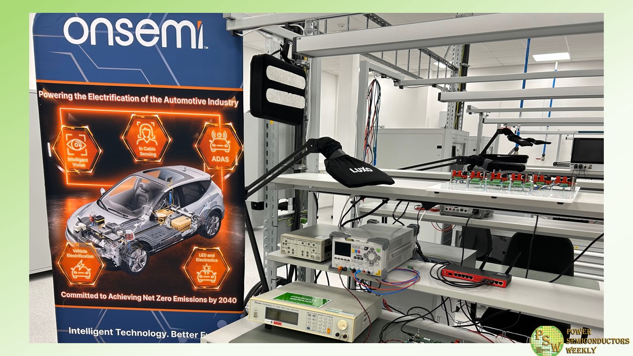
onsemi opened an application test lab in Piestany, Slovakia, focused on the advancement of system solutions for battery/plug-in hybrid/electric vehicles (xEVs) and energy infrastructure (EI) power conversion systems. The state-of-the-art systems applications lab provides specialized equipment to develop and test next-generation silicon (Si) and silicon carbide (SiC) semiconductor solutions in collaboration with automotive OEMs, Tier 1s and EI providers.
Modern semiconductor devices are essential for highly efficient power conversion in xEV powertrains and charging, as well as applications in renewable energy. The new lab will play a central role in ensuring that the development of future power products results in highly differentiated, value-add solutions tailored to customers’ specific requirements.
The new facility consists of two high-voltage power labs that focus on systems and device level development as well as evaluation of SiC/Si traction inverters and ACDC/DCDC power converters. Laser welding facilities, mechanical clean rooms and workshops further enable fast prototyping and testing of next-generation system solutions.
Evaluation capabilities for the next-generation system solutions include:
- Continuous 24/7 testing
- Internally developed and patented software and hardware solutions to support high-voltage power cycling via space vector modulation (SVM) and sinusoidal pulse width modulation (SPWM)
- High-accuracy logging devices for assessing SiC and Si health and reliability
- Simulation of the harsh conditions faced by inverters during operation, testing liquid-cooled devices at temperatures as low as minus 50 degrees C and up to 220 degrees C
- Wider range of industry-recognized software allows for the programing of FPGAs and ARM microcontrollers on site, as well as qualification testing, data analysis and 3D modeling
Original – onsemi
-
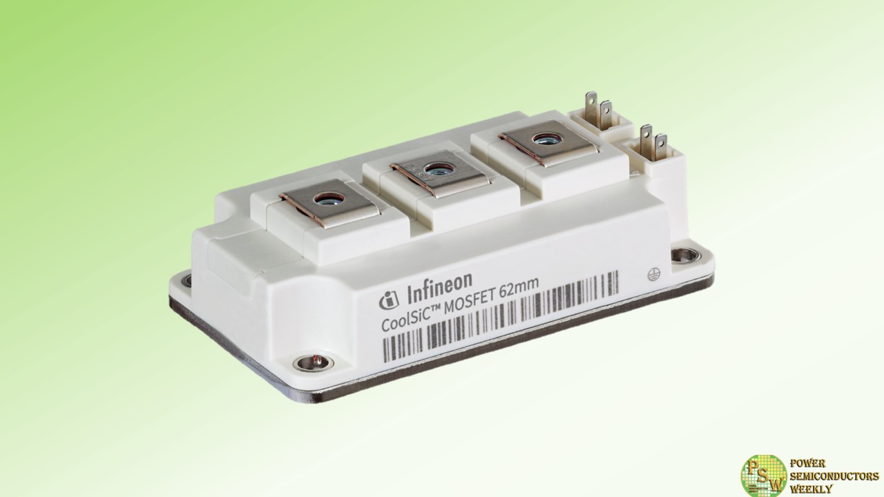
Infineon Technologies AG announced the expansion of its CoolSiC 1200 V and 2000 V MOSFET module families with a new industry-standard package. The proven 62mm device is designed in half-bridge topology and is based on the recently introduced and advanced M1H silicon carbide (SiC) MOSFET technology.
The package enables the use of SiC for mid-power applications from 250 kW – where silicon reaches the limits of power density with IGBT technology. Compared to a 62mm IGBT module, the list of applications now additionally includes solar, server, energy storage, EV charger, traction, commercial induction cooking and power conversion systems.
The M1H technology enables a significantly wider gate voltage window, ensuring high robustness to driver and layout-induced voltage spikes at the gate without any restrictions even at high switching frequencies. In addition to that, very low switching and transmission losses minimize cooling requirements.
Combined with a high reverse voltage, these devices meet another requirement of modern system design. By using Infineon’s CoolSiC chip technology, converter designs can be made more efficient, the nominal power per inverter can be increased and system costs can be reduced.
With baseplate and screw connections, the package features a very rugged mechanical design optimized for highest system availability, minimum service costs and downtime losses. Outstanding reliability is achieved through high thermal cycling capability and a continuous operating temperature (T vjop) of 150°C. The symmetrical internal package design provides identical switching conditions for the upper and lower switches. Optionally, the thermal performance of the module can be further enhanced with pre-applied thermal interface material (TIM).
The CoolSiC 62mm package MOSFETs are available in 1200 V variants of 5 mΩ/180 A, 2 mΩ/420 A and 1 mΩ/560 A. The 2000 V portfolio will include the 4 mΩ/300 A and 3 mΩ/400 A variants. The portfolio will be completed in Q1 2024 with the 1200 V/3 mΩ and 2000 V/5 mΩ variants.
An evaluation board is available for rapid characterization of the modules (double pulse/continuous operation). For ease of use, it provides flexible adjustment of the gate voltage and gate resistors. At the same time, it can be used as a reference design for driver boards for volume production.
Original – Infineon Technologies
-
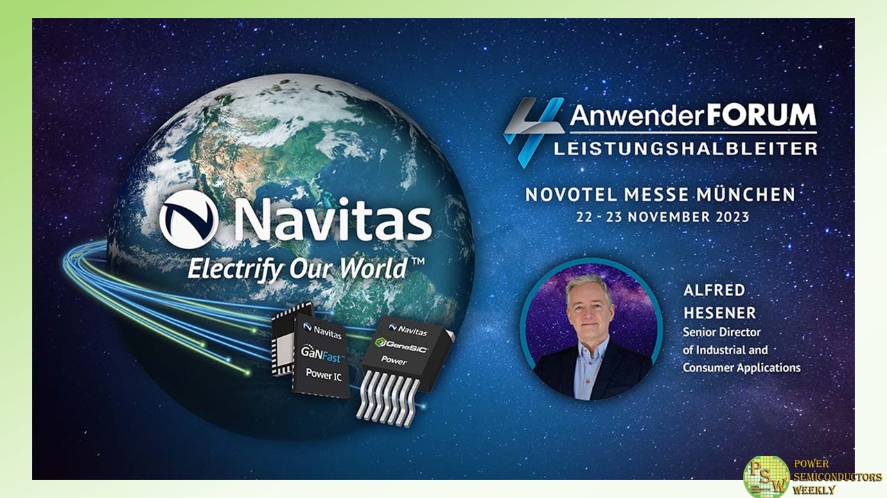
Navitas Semiconductor announced its participation in the Power Semiconductor User Forum, organized by WEKA Fachmedien on November 22nd -23rd, 2023. The event offers valuable insights into power electronics for developers and technical buyers.
Alfred Hesener, Senior Director of Industrial and Consumer Applications will explore “Reliability and Cost-of-Ownership Optimization in Industrial Power Supplies,” on November 23rd at 1:45 p.m. CET. Mr. Hesener will highlight next-generation solutions that achieve high power densities, cool operation, robust performance using Navitas’ GaNSense single and Half-Bridge power ICs.
Navitas’ GaNFast power ICs integrate GaN power and drive with control, sensing, and protection to enable faster charging, higher power density, greater energy savings and system cost reduction. In addition, each GaN power IC saves over 4 kg CO2 due to higher efficiency and dematerialization. New ‘Gen-3 Fast’ GeneSiC MOSFETs have up to 50% improved performance vs. other SiC devices, and save over 40 kg CO2 per unit vs. legacy silicon IGBTs.
“For industrial power designers, the WEKA forum highlights leading-edge, reliable technology for drives, pumps, chargers and power conversion, using GaN and SiC,” said Mr. Hesener. “Features like loss-less current sensing, programmable dV/dt, 2 kV ESD protection and autonomous sensing and protection are key enablers, and reduce time to market.”
WEKA Fachmedien’s Power Semiconductor User Forum 2023 will be held from November 22nd-23rd at the Novotel Messe Munich, Willy-Brandt-Platz 1, 81829 München, Germany.
Original – Navitas Semiconductor
-
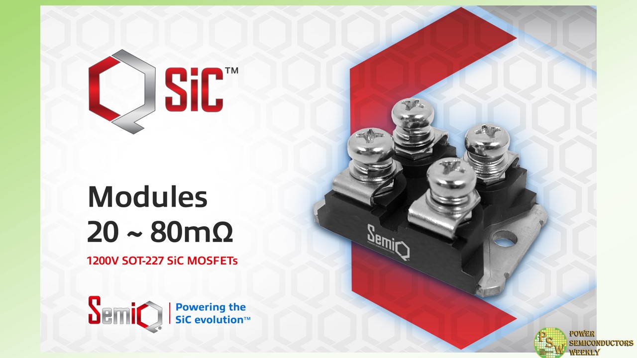
SemiQ announced that it has expanded its portfolio of QSiC™ Silicon Carbide modules with the launch of a family of 1200V MOSFETs that pairs with or without 1200V SiC Schottky Diodes in a SOT-227 package.
Crafted from high-performance ceramics and rigorously engineered to function with unwavering reliability in challenging conditions, the newly introduced SemiQ SiC modules achieve remarkably high performance. This enhanced performance empowers higher power densities and more streamlined design configurations.
The QSiC™ modules feature high breakdown voltage (> 1400 V), high-temperature operation (Tj = 175 °C), and low Rds(On) shift over the full operating temperature range while providing industry-leading gate oxide stability and gate oxide lifetime, avalanche (UIS) ruggedness, and extended short-circuit withstand times.
Target markets for the new QSiC™ modules with our existing SOT-227 SiC SBD modules include EV charging, on-board chargers (OBCs), DC-DC converters, E-compressors, fuel cell converters, medical power supplies, energy storage systems, solar and wind energy systems, data center power supplies, UPS/PFC circuits, and other automotive and industrial power applications.
All of the new QSiC™ modules are tested at wafer-level gate burn-in to provide high-quality gate oxide with stable gate threshold voltage. Besides the burn-in test, which helps to stabilize the extrinsic failure rate, stress tests such as gate stress, high-temperature reverse bias (HTRB) drain stress, and high humidity, high voltage, high temperature (H3TRB) to ensure requisite industrial grade quality levels.
Dr. Timothy Han, President at SemiQ, said, “We are delighted with the customer input and needs for our new family of QSiC™ high-power modules and thank our SemiQ team who have worked tirelessly to build and qualify our latest QSiC™ modules.”
SemiQ’s new 1200V SOT-227 modules are available in 20mΩ, 40mΩ, 80mΩ SiC MOSFET categories. A table with part numbers is shown below.
Part Numbers Circuit Configuration Ratings, Packages Rds(on), mΩ GCMX020B120S1-E1 Single MOSFET w/o SBD 1200V/113A, SOT-227 20 GCMS020B120S1-E1 Single MOSFET w SBD 1200V/113A, SOT-227 20 GCMX040B120S1-E1 Single MOSFET w/o SBD 1200V/57A, SOT-227 40 GCMS040B120S1-E1 Single MOSFET w SBD 1200V/57A, SOT-227 40 GCMX080B120S1-E1 Single MOSFET w/o SBD 1200V/30A, SOT-227 80 GCMS080B120S1-E1 Single MOSFET w SBD 1200V/30A, SOT-227 80 Original – SemiQ
-

Soitec announced its revenue for the second quarter of fiscal year 2024 and its results for the first half of fiscal year 2024 (ended on September 30th, 2023). The financial statements were approved by the Board of Directors during its meeting today.
- Q2’24 revenue reached €245m, down 7% at constant exchange rates and perimeter compared to Q2’23
- H1’24 revenue at €401m, down 15% both at constant exchange rates and perimeter and on a reported basis compared with H1’23 – in line with guidance
- H1’24 EBITDA margin stood at the robust level of 33% of revenue while the Company maintained significant investment in R&D
- Anticipated return to a slight year-on-year organic growth in H2’24, leading to a moderate downward revision of FY24 outlook: mid-single digit decline in FY’24 revenue expected at constant exchange rate and EBITDA1 margin2 anticipated around 35%
Pierre Barnabé, Soitec’s CEO, commented: “With a sequential growth of over 50% compared to the first quarter, our second-quarter revenue rebounded significantly, as we had anticipated. This was particularly the case in Mobile Communications as the inventory correction across the smartphone value chain eased. We continue to leverage strong demand in Automotive to deploy our SmartSiC™roadmap and we continue to progress actively with several customers.
Overall, our first half revenue is in line with our expectations. We have maintained strong profitability and a solid financial position, while continuing to invest in R&D and industrial capacity, as well as building inventories to prepare for H2’24.
Looking ahead, we maintain our growth perspectives for the second part of the fiscal year. We note however that the absorption of RF-SOI inventories at our customers level will last longer than anticipated. At the same time, we continue to expect sustained demand in Automotive & Industrial as well as in Smart Devices. Consequently, we now anticipate a full-fiscal-year revenue decline of around mid-single digit percentage, and an EBITDA margin of around 35%. After this transition year, we will resume our growth trajectory” added Pierre Barnabé.
FY’24 outlook
Soitec confirms growth recovery in the second half of FY’24. Against the backdrop of a weaker-than-expected smartphone market, the extent of the inventory correction at our customers level is greater than anticipated. We confirm strong traction for our Automotive & Industrial and Smart Devices divisions. We now anticipate our FY’24 revenue to slightly decline, by around a mid-single digit percentage, compared to FY’23, at constant exchange rates and perimeter.
As a result, FY’24 EBITDA margin is now expected to be around 35% of revenue. The Group will continue to implement cost control measures, while further investing significantly in R&D.
FY’24 Capital expenditure is expected to be around 290 million Euros in order to support growth beyond FY’24. Soitec’s growth outlook remain very strong: while the SOI content within end devices continues to increase, the ongoing penetration of the Group’s products across its three end markets and the successful deployment of its expansion into Compound Semiconductors with POI and SmartSiC™ becoming new significant growth drivers in the future.
Original – Soitec
-

The Hanau-based technology company Heraeus has acquired a significant stake in the start-up company Zadient. Heraeus, as a German high-tech materials player considers the market of SiC base material highly relevant and a suitable addition to its other operations.
The French-German firm Zadient specializes in the production of silicon carbide source material. Silicon carbide is a wide band gap semiconductor material, which is currently gaining rapid traction in the semiconductor market. Its properties lend themselves to use in power semiconductors, which help to convert current and voltages.
Its fundamental contribution is the dramatic increase in efficiency it provides over silicon by reducing the heat losses that occur while power passes through chips. Its ability to handle higher power densities with low losses allows for the transition from 400V to 800V battery systems in EVs which significantly shortens their charging time and increases their range. SiC based electronics are also smaller and lighter, which also contributes to increased range.
These properties have lead to the rapid adoption of SiC in applications ranging from the main inverters and on-board chargers in EVs to wind and solar power inverters, battery storage systems and even airplane power management modules. The breadth of these few examples is already an indication of the significant role SiC will play in the mobility and energy transition.
Through the partnership, Heraeus intends to accelerate the company’s growth and support Zadient’s innovative approach with its own know-how.
“Heraeus recognizes the potential of the SiC market and considers it to be highly relevant for high-tech applications. By acquiring a stake in Zadient, we can jointly offer our customers even better solutions” said Steffen Metzger, member of the Heraeus Group Management Committee. “We are very happy that we found a way to accelerate growth in the SiC market by combining the innovative ideas of the materials start-up Zadient with the manufacturing and technical expertise of the Heraeus Group.”
“We are very excited to be partnering with an industry leader like Heraeus,” noted Zadient CEO Kagan Ceran. “The expertise that Heraeus has in the industrial scale production of advanced materials, both in its home market of Germany and abroad, offers us unique synergies as we strive to realize our vision to be the world’s largest volume, highest purity producer of silicon carbide semiconductor materials.”
Original – Heraeus
-
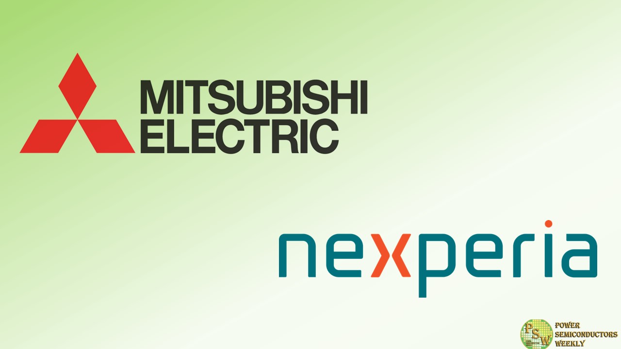
Mitsubishi Electric Corporation announced that it will enter into a strategic partnership with Nexperia B.V. to jointly develop silicon carbide (SiC) power semiconductors for the power electronics market. Mitsubishi Electric will leverage its wide-bandgap semiconductor technologies to develop and supply SiC MOSFET chips that Nexperia will use to develop SiC discrete devices.
The electric vehicle market is expanding worldwide and is helping to drive the exponential growth of SiC power semiconductors, which offer lower energy loss, higher operating temperatures and faster switching speeds than conventional silicon power semiconductors. The high efficiency of SiC power semiconductors is expected to contribute significantly to global decarbonization and green transformation.
Mitsubishi Electric has established leading positions in applications such as high-speed trains, high-voltage industrial applications and home appliances. The company launched the world’s first SiC power modules for air conditioners in 2010 and became the first supplier of an all-SiC power module for Shinkansen bullet trains in 2015. Mitsubishi Electric has accumulated superior expertise for the development and manufacture of SiC power modules, which are known for their advanced performance and high reliability.
Going forward, Mitsubishi Electric expects to strengthen its partnership with Nexperia, a global leader with decades of experience in the design, manufacture, quality assurance and supply of diverse discrete devices. Nexperia’s devices are used in the automotive, industrial, mobile and consumer markets, contributing to decarbonization and a more sustainable future. Mitsubishi Electric will continue to improve the performance and quality of its SiC chips and focus on the development of power modules using proprietary module technologies.
Mark Roeloffzen, SVP & General Manager Business Group Bipolar Discretes at Nexperia, said: “This mutually beneficial strategic partnership with Mitsubishi Electric represents a significant stride in Nexperia’s silicon carbide journey. Mitsubishi Electric has a strong track record as a supplier of technically proven SiC device and modules. Combined with Nexperia’s high-quality standards and expertise in discrete products and packaging, we will certainly generate positive synergies between both companies – ultimately enabling our customers to deliver highly energy efficient products in the industrial, automotive or consumer markets they serve.”
Masayoshi Takemi, Executive Officer and Group President, Semiconductor & Device at Mitsubishi Electric, said: “Nexperia is a leading company in the industrial sector with proven technologies for high quality discrete semiconductors. We are delighted to enter into this co-development partnership that will leverage the semiconductor technologies of both companies.”
Original – Mitsubishi Electric
-
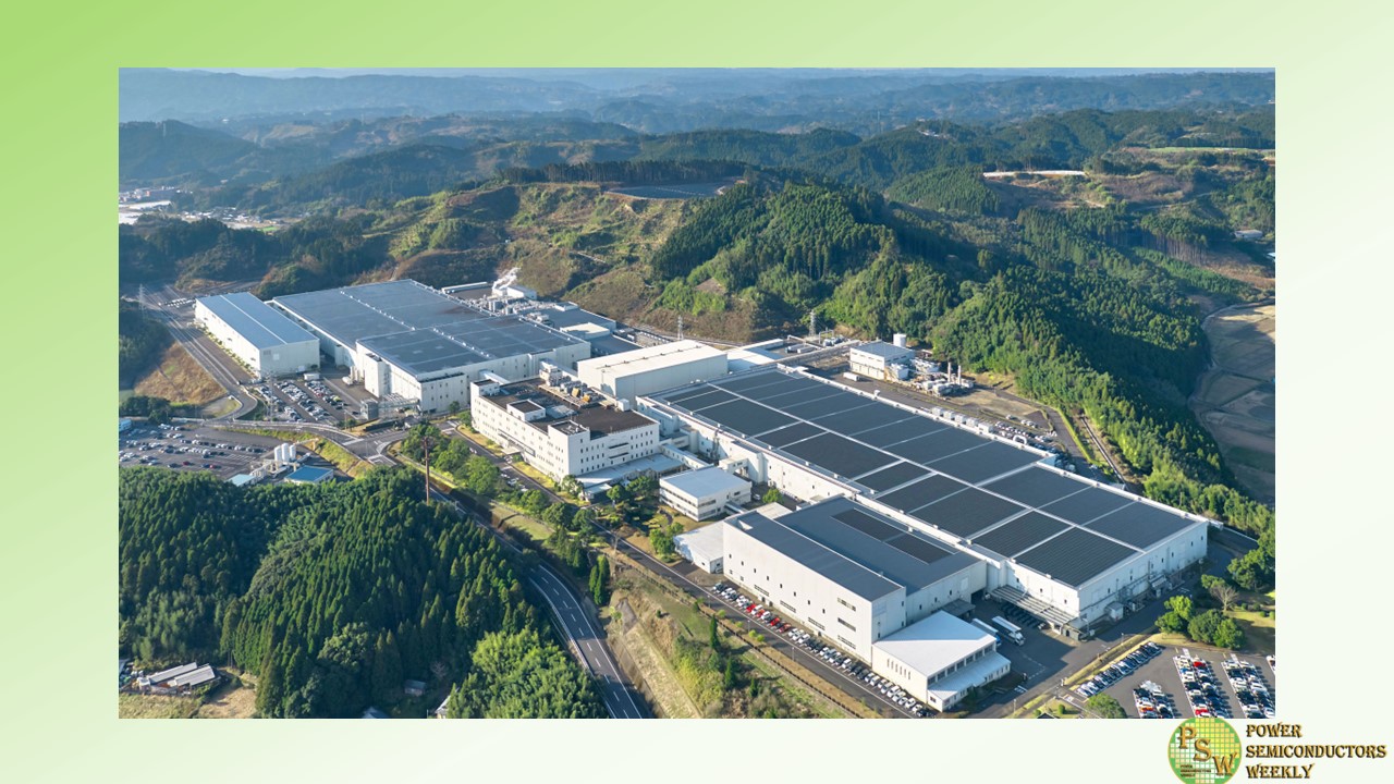
ROHM has completed the acquisition of the assets of Solar Frontier’s former Kunitomi Plant located in Japan, on November 7, 2023, based on its basic agreement signed with Solar Frontier.
The Plant will be operated by LAPIS Semiconductor, a subsidiary of the ROHM Group, as its Miyazaki Plant No.2. It will become the Group’s main production site for SiC power devices and is aiming to start operation during 2024.
The ROHM Group will continue to strengthen its production capacity in accordance with its Medium-Term Management Plan while keeping abreast of market conditions, and will also thoroughly enhance its BCM system to ensure a stable supply of products to customers.
Original – ROHM
